JP2008510966A - How to make wire bond probe cards in multiple ways at once - Google Patents
How to make wire bond probe cards in multiple ways at once Download PDFInfo
- Publication number
- JP2008510966A JP2008510966A JP2007528044A JP2007528044A JP2008510966A JP 2008510966 A JP2008510966 A JP 2008510966A JP 2007528044 A JP2007528044 A JP 2007528044A JP 2007528044 A JP2007528044 A JP 2007528044A JP 2008510966 A JP2008510966 A JP 2008510966A
- Authority
- JP
- Japan
- Prior art keywords
- substrate
- support substrate
- contact element
- spring contact
- contact
- Prior art date
- Legal status (The legal status is an assumption and is not a legal conclusion. Google has not performed a legal analysis and makes no representation as to the accuracy of the status listed.)
- Pending
Links
Images


Classifications
-
- G—PHYSICS
- G01—MEASURING; TESTING
- G01R—MEASURING ELECTRIC VARIABLES; MEASURING MAGNETIC VARIABLES
- G01R1/00—Details of instruments or arrangements of the types included in groups G01R5/00 - G01R13/00 and G01R31/00
- G01R1/02—General constructional details
- G01R1/06—Measuring leads; Measuring probes
- G01R1/067—Measuring probes
-
- G—PHYSICS
- G01—MEASURING; TESTING
- G01R—MEASURING ELECTRIC VARIABLES; MEASURING MAGNETIC VARIABLES
- G01R3/00—Apparatus or processes specially adapted for the manufacture or maintenance of measuring instruments, e.g. of probe tips
-
- G—PHYSICS
- G01—MEASURING; TESTING
- G01R—MEASURING ELECTRIC VARIABLES; MEASURING MAGNETIC VARIABLES
- G01R1/00—Details of instruments or arrangements of the types included in groups G01R5/00 - G01R13/00 and G01R31/00
- G01R1/02—General constructional details
- G01R1/06—Measuring leads; Measuring probes
- G01R1/067—Measuring probes
- G01R1/073—Multiple probes
- G01R1/07307—Multiple probes with individual probe elements, e.g. needles, cantilever beams or bump contacts, fixed in relation to each other, e.g. bed of nails fixture or probe card
- G01R1/07342—Multiple probes with individual probe elements, e.g. needles, cantilever beams or bump contacts, fixed in relation to each other, e.g. bed of nails fixture or probe card the body of the probe being at an angle other than perpendicular to test object, e.g. probe card
-
- G—PHYSICS
- G01—MEASURING; TESTING
- G01R—MEASURING ELECTRIC VARIABLES; MEASURING MAGNETIC VARIABLES
- G01R1/00—Details of instruments or arrangements of the types included in groups G01R5/00 - G01R13/00 and G01R31/00
- G01R1/02—General constructional details
- G01R1/06—Measuring leads; Measuring probes
- G01R1/067—Measuring probes
- G01R1/073—Multiple probes
- G01R1/07307—Multiple probes with individual probe elements, e.g. needles, cantilever beams or bump contacts, fixed in relation to each other, e.g. bed of nails fixture or probe card
- G01R1/07364—Multiple probes with individual probe elements, e.g. needles, cantilever beams or bump contacts, fixed in relation to each other, e.g. bed of nails fixture or probe card with provisions for altering position, number or connection of probe tips; Adapting to differences in pitch
- G01R1/07378—Multiple probes with individual probe elements, e.g. needles, cantilever beams or bump contacts, fixed in relation to each other, e.g. bed of nails fixture or probe card with provisions for altering position, number or connection of probe tips; Adapting to differences in pitch using an intermediate adapter, e.g. space transformers
-
- G—PHYSICS
- G01—MEASURING; TESTING
- G01R—MEASURING ELECTRIC VARIABLES; MEASURING MAGNETIC VARIABLES
- G01R31/00—Arrangements for testing electric properties; Arrangements for locating electric faults; Arrangements for electrical testing characterised by what is being tested not provided for elsewhere
- G01R31/26—Testing of individual semiconductor devices
-
- H—ELECTRICITY
- H01—ELECTRIC ELEMENTS
- H01L—SEMICONDUCTOR DEVICES NOT COVERED BY CLASS H10
- H01L22/00—Testing or measuring during manufacture or treatment; Reliability measurements, i.e. testing of parts without further processing to modify the parts as such; Structural arrangements therefor
-
- G—PHYSICS
- G01—MEASURING; TESTING
- G01R—MEASURING ELECTRIC VARIABLES; MEASURING MAGNETIC VARIABLES
- G01R31/00—Arrangements for testing electric properties; Arrangements for locating electric faults; Arrangements for electrical testing characterised by what is being tested not provided for elsewhere
- G01R31/28—Testing of electronic circuits, e.g. by signal tracer
- G01R31/2851—Testing of integrated circuits [IC]
- G01R31/2886—Features relating to contacting the IC under test, e.g. probe heads; chucks
- G01R31/2889—Interfaces, e.g. between probe and tester
-
- H—ELECTRICITY
- H01—ELECTRIC ELEMENTS
- H01L—SEMICONDUCTOR DEVICES NOT COVERED BY CLASS H10
- H01L2224/00—Indexing scheme for arrangements for connecting or disconnecting semiconductor or solid-state bodies and methods related thereto as covered by H01L24/00
- H01L2224/01—Means for bonding being attached to, or being formed on, the surface to be connected, e.g. chip-to-package, die-attach, "first-level" interconnects; Manufacturing methods related thereto
- H01L2224/42—Wire connectors; Manufacturing methods related thereto
- H01L2224/47—Structure, shape, material or disposition of the wire connectors after the connecting process
- H01L2224/48—Structure, shape, material or disposition of the wire connectors after the connecting process of an individual wire connector
- H01L2224/4805—Shape
- H01L2224/4809—Loop shape
- H01L2224/48091—Arched
-
- H—ELECTRICITY
- H01—ELECTRIC ELEMENTS
- H01L—SEMICONDUCTOR DEVICES NOT COVERED BY CLASS H10
- H01L2224/00—Indexing scheme for arrangements for connecting or disconnecting semiconductor or solid-state bodies and methods related thereto as covered by H01L24/00
- H01L2224/01—Means for bonding being attached to, or being formed on, the surface to be connected, e.g. chip-to-package, die-attach, "first-level" interconnects; Manufacturing methods related thereto
- H01L2224/42—Wire connectors; Manufacturing methods related thereto
- H01L2224/47—Structure, shape, material or disposition of the wire connectors after the connecting process
- H01L2224/49—Structure, shape, material or disposition of the wire connectors after the connecting process of a plurality of wire connectors
- H01L2224/491—Disposition
- H01L2224/4912—Layout
- H01L2224/49171—Fan-out arrangements
-
- H—ELECTRICITY
- H01—ELECTRIC ELEMENTS
- H01L—SEMICONDUCTOR DEVICES NOT COVERED BY CLASS H10
- H01L2924/00—Indexing scheme for arrangements or methods for connecting or disconnecting semiconductor or solid-state bodies as covered by H01L24/00
- H01L2924/01—Chemical elements
- H01L2924/01019—Potassium [K]
-
- H—ELECTRICITY
- H01—ELECTRIC ELEMENTS
- H01L—SEMICONDUCTOR DEVICES NOT COVERED BY CLASS H10
- H01L2924/00—Indexing scheme for arrangements or methods for connecting or disconnecting semiconductor or solid-state bodies as covered by H01L24/00
- H01L2924/01—Chemical elements
- H01L2924/01046—Palladium [Pd]
-
- H—ELECTRICITY
- H01—ELECTRIC ELEMENTS
- H01L—SEMICONDUCTOR DEVICES NOT COVERED BY CLASS H10
- H01L2924/00—Indexing scheme for arrangements or methods for connecting or disconnecting semiconductor or solid-state bodies as covered by H01L24/00
- H01L2924/01—Chemical elements
- H01L2924/01057—Lanthanum [La]
-
- H—ELECTRICITY
- H01—ELECTRIC ELEMENTS
- H01L—SEMICONDUCTOR DEVICES NOT COVERED BY CLASS H10
- H01L2924/00—Indexing scheme for arrangements or methods for connecting or disconnecting semiconductor or solid-state bodies as covered by H01L24/00
- H01L2924/01—Chemical elements
- H01L2924/01078—Platinum [Pt]
-
- H—ELECTRICITY
- H01—ELECTRIC ELEMENTS
- H01L—SEMICONDUCTOR DEVICES NOT COVERED BY CLASS H10
- H01L2924/00—Indexing scheme for arrangements or methods for connecting or disconnecting semiconductor or solid-state bodies as covered by H01L24/00
- H01L2924/01—Chemical elements
- H01L2924/01079—Gold [Au]
-
- H—ELECTRICITY
- H01—ELECTRIC ELEMENTS
- H01L—SEMICONDUCTOR DEVICES NOT COVERED BY CLASS H10
- H01L2924/00—Indexing scheme for arrangements or methods for connecting or disconnecting semiconductor or solid-state bodies as covered by H01L24/00
- H01L2924/10—Details of semiconductor or other solid state devices to be connected
- H01L2924/102—Material of the semiconductor or solid state bodies
- H01L2924/1025—Semiconducting materials
- H01L2924/10251—Elemental semiconductors, i.e. Group IV
- H01L2924/10253—Silicon [Si]
-
- H—ELECTRICITY
- H01—ELECTRIC ELEMENTS
- H01L—SEMICONDUCTOR DEVICES NOT COVERED BY CLASS H10
- H01L2924/00—Indexing scheme for arrangements or methods for connecting or disconnecting semiconductor or solid-state bodies as covered by H01L24/00
- H01L2924/10—Details of semiconductor or other solid state devices to be connected
- H01L2924/11—Device type
- H01L2924/12—Passive devices, e.g. 2 terminal devices
- H01L2924/1204—Optical Diode
- H01L2924/12041—LED
-
- H—ELECTRICITY
- H01—ELECTRIC ELEMENTS
- H01L—SEMICONDUCTOR DEVICES NOT COVERED BY CLASS H10
- H01L2924/00—Indexing scheme for arrangements or methods for connecting or disconnecting semiconductor or solid-state bodies as covered by H01L24/00
- H01L2924/10—Details of semiconductor or other solid state devices to be connected
- H01L2924/11—Device type
- H01L2924/14—Integrated circuits
-
- H—ELECTRICITY
- H01—ELECTRIC ELEMENTS
- H01L—SEMICONDUCTOR DEVICES NOT COVERED BY CLASS H10
- H01L2924/00—Indexing scheme for arrangements or methods for connecting or disconnecting semiconductor or solid-state bodies as covered by H01L24/00
- H01L2924/19—Details of hybrid assemblies other than the semiconductor or other solid state devices to be connected
- H01L2924/1901—Structure
- H01L2924/1904—Component type
- H01L2924/19041—Component type being a capacitor
-
- H—ELECTRICITY
- H01—ELECTRIC ELEMENTS
- H01L—SEMICONDUCTOR DEVICES NOT COVERED BY CLASS H10
- H01L2924/00—Indexing scheme for arrangements or methods for connecting or disconnecting semiconductor or solid-state bodies as covered by H01L24/00
- H01L2924/30—Technical effects
- H01L2924/301—Electrical effects
- H01L2924/3011—Impedance
- H01L2924/30111—Impedance matching
-
- Y—GENERAL TAGGING OF NEW TECHNOLOGICAL DEVELOPMENTS; GENERAL TAGGING OF CROSS-SECTIONAL TECHNOLOGIES SPANNING OVER SEVERAL SECTIONS OF THE IPC; TECHNICAL SUBJECTS COVERED BY FORMER USPC CROSS-REFERENCE ART COLLECTIONS [XRACs] AND DIGESTS
- Y10—TECHNICAL SUBJECTS COVERED BY FORMER USPC
- Y10T—TECHNICAL SUBJECTS COVERED BY FORMER US CLASSIFICATION
- Y10T29/00—Metal working
- Y10T29/49—Method of mechanical manufacture
- Y10T29/49002—Electrical device making
- Y10T29/49117—Conductor or circuit manufacturing
- Y10T29/49121—Beam lead frame or beam lead device
-
- Y—GENERAL TAGGING OF NEW TECHNOLOGICAL DEVELOPMENTS; GENERAL TAGGING OF CROSS-SECTIONAL TECHNOLOGIES SPANNING OVER SEVERAL SECTIONS OF THE IPC; TECHNICAL SUBJECTS COVERED BY FORMER USPC CROSS-REFERENCE ART COLLECTIONS [XRACs] AND DIGESTS
- Y10—TECHNICAL SUBJECTS COVERED BY FORMER USPC
- Y10T—TECHNICAL SUBJECTS COVERED BY FORMER US CLASSIFICATION
- Y10T29/00—Metal working
- Y10T29/49—Method of mechanical manufacture
- Y10T29/49002—Electrical device making
- Y10T29/49117—Conductor or circuit manufacturing
- Y10T29/49124—On flat or curved insulated base, e.g., printed circuit, etc.
- Y10T29/49147—Assembling terminal to base
-
- Y—GENERAL TAGGING OF NEW TECHNOLOGICAL DEVELOPMENTS; GENERAL TAGGING OF CROSS-SECTIONAL TECHNOLOGIES SPANNING OVER SEVERAL SECTIONS OF THE IPC; TECHNICAL SUBJECTS COVERED BY FORMER USPC CROSS-REFERENCE ART COLLECTIONS [XRACs] AND DIGESTS
- Y10—TECHNICAL SUBJECTS COVERED BY FORMER USPC
- Y10T—TECHNICAL SUBJECTS COVERED BY FORMER US CLASSIFICATION
- Y10T29/00—Metal working
- Y10T29/49—Method of mechanical manufacture
- Y10T29/49002—Electrical device making
- Y10T29/49117—Conductor or circuit manufacturing
- Y10T29/49204—Contact or terminal manufacturing
- Y10T29/49224—Contact or terminal manufacturing with coating
Abstract
非常に微細なピッチ間隔で製造できかつ支持基板に正確に配置できる、ウエハテストプロービングで用いるための弾性ばね接点が、提供される。弾性接触構造体は、スペース変換基板上の電気回路へのワイヤボンディング用に適合されている。付着ばね接点を備えた支持基板を一緒に数多く製造し、スペース変換基板へ付着させる前にダイシングおよびテストをして、歩留まりを改善することができる。弾性ばね接点は、剥離層上に接点を形成するためにフォトリソグラフィ技術を用いて製造され、その後ばね接点は、支持基板にエポキシで接着され、剥離層は除去される。支持基板は、接点の整列および下方の光学部品のテストを可能にするために、透明にすることができる。支持基板には、インピーダンス整合の改善のために、ばね接点の下に設けられた接地プレートを含むことができる。 Elastic spring contacts are provided for use in wafer test probing that can be manufactured with very fine pitch spacing and can be accurately placed on a support substrate. The resilient contact structure is adapted for wire bonding to an electrical circuit on the space conversion substrate. Many support substrates with attachment spring contacts can be manufactured together and diced and tested prior to attachment to the space conversion substrate to improve yield. The elastic spring contact is manufactured using photolithography techniques to form a contact on the release layer, after which the spring contact is epoxy bonded to the support substrate and the release layer is removed. The support substrate can be transparent to allow contact alignment and testing of the underlying optical components. The support substrate can include a ground plate provided under the spring contact for improved impedance matching.
Description
技術分野
本発明は、電気部品間の圧力接触をもたらす弾性電気接触要素またはばね接点に関し、特に、ウエハ上の集積回路(IC)をテストするプロービングに用いるプローブカードを形成するばね接点およびばね接点を基板に付着させるための構造体に関する。
TECHNICAL FIELD The present invention relates to elastic electrical contact elements or spring contacts that provide pressure contact between electrical components, and in particular to spring contacts and spring contacts that form a probe card for use in probing to test an integrated circuit (IC) on a wafer. The present invention relates to a structure for attaching to a substrate.
関連技術
弾性接触要素またはばね接点は、様々な形状で製造される。ウエハ上のICをプロービングするために用いられる一タイプのばね接点が、「犠牲部材を用いた、電気接点の製造方法(Method of Manufacturing Electrical Contacts, Using a Sacrificial Member)」なる名称の米国特許第5,476,211号明細書ならびにその対応分割特許である米国特許第5,852,871号明細書および米国特許第6,049,976号明細書(全てカンドロス(Khandros)による)に説明されている。これらの特許は、フレキシブルで細長いコア要素(たとえばワイヤ「ステム」または「スケルトン」)を電子部品の端子に取り付けること、および1つまたは複数の材料の「シェル」でフレキシブルコア要素をコーティングし、結果として得られるばね接点の弾性特性を保証することによって、弾性相互接続要素を作製する方法を開示している。コア要素の例示的な材料には、金が含まれる。弾性コーティングの例示的な材料には、ニッケルおよびその合金が含まれる。結果として得られるばね接触要素は、プローブカードとウエハ上の集積回路との間をはじめとして2以上の電子部品間の圧力接続をもたらすために用いられる。
Related Art Elastic contact elements or spring contacts are manufactured in various shapes. One type of spring contact used for probing an IC on a wafer is US Pat. No. 5, entitled “Method of Manufacturing Electrical Contacts, Using a Scientific Member” using a sacrificial member. No. 4,476,211 and its corresponding divisional patents US Pat. No. 5,852,871 and US Pat. No. 6,049,976 (all by Khandros). . These patents attach a flexible, elongated core element (eg, a wire “stem” or “skeleton”) to a terminal of an electronic component, and coat the flexible core element with a “shell” of one or more materials, resulting in Discloses a method for making an elastic interconnecting element by ensuring the elastic properties of the resulting spring contact. Exemplary materials for the core element include gold. Exemplary materials for the elastic coating include nickel and its alloys. The resulting spring contact element is used to provide a pressure connection between two or more electronic components, including between the probe card and the integrated circuit on the wafer.
基板にばね接点を接続してプローブカード、またはばね接点を備えた他の構造体を形成することが、エルドリッジ(Eldridge)、グルーベ(Grube)、カンドロス(Khandros)およびマシュー(Mathieu)による「プローブカードアセンブリのプローブ要素の先端を平坦化する方法(Method of Planarizing Tips of Probe Elements of a Probe Card Assembly)」なる名称の米国特許第5,974,662号明細書に説明されている。この特許は、「スペース変換器」を形成するために細長い弾性ばね接触要素を取り付けた基板をはじめとして、プローブカードアセンブリについて説明している。スペース変換器は、一表面において、端子を第1のピッチまたは端子間の間隔に配置し、かつ反対表面における第2のピッチに、対応する端子を配置した多層相互接続基板である。スペース変換は、第1のピッチから第2のピッチへ「ピッチ拡張」を達成するために用いられる基板の層におけるルーティング線によって提供される。使用において、細長いばね接触要素の自由端(先端)が、プロービングまたはテストされる電子部品の対応する端子との圧力接続をもたらす。 Connecting a spring contact to a substrate to form a probe card, or other structure with spring contacts, is a "probe card" by Eldridge, Grube, Khandros, and Mathieu U.S. Pat. No. 5,974,662, entitled “Method of Planarizing Tips of Probe Elements of a Probe Card Assembly”. This patent describes a probe card assembly, including a substrate with an elongated elastic spring contact element attached to form a “space transducer”. A space transducer is a multilayer interconnect substrate having terminals on one surface with a first pitch or spacing between terminals and corresponding terminals on a second pitch on the opposite surface. Space conversion is provided by routing lines in the layer of the substrate used to achieve “pitch expansion” from the first pitch to the second pitch. In use, the free end (tip) of the elongated spring contact element provides a pressure connection with the corresponding terminal of the electronic component to be probed or tested.
別のタイプのばね接触要素が、エルドリッジ(Eldridge)、グルーベ(Grube)、カンドロス(Khandros)およびマシュー(Mathieu)による「マイクロエレクトロニクスばね接触要素および複数のばね接触要素を有する電子部品(Microelectronic Spring Contact Element and Electronic Component Having A Plurality Of Spring Contact Elements)」なる名称の米国特許第6,482,013号明細書に説明されており、この特許は、参照により本明細書に援用されている。この特許は、弾性接触要素を作製するために、機械技術ではなくフォトリソグラフィ技術について説明している。機械的に形成された接触要素と同様に、リソグラフィ技術を用いて形成された弾性接触要素には、ニッケルおよびその合金などの弾性材料が含まれる。フォトリソグラフィ技術を用いて、弾性接点を備えたプローブカードまたは他の基板を製造するために、ばね接点が、材料のめっきまたは堆積、フォトレジストの適用、フォトリソグラフィ技術を用いたマスキング、およびエッチングを含む一連のステップによって、基板表面の金属相互接続パッドに形成される。スペース変換器については、弾性接点が自身に形成された相互接続パッドは、スペース変換基板内のルーティング線に弾性接点を接続する。フォトリソグラフィ技術を用いれば、精密許容誤差を実現して、パッドに形成されたばね接点と、テストされる集積回路上の対応する接触パッドとの整列を保証することができる。 Another type of spring contact element is "Microelectronic Spring Contact Element by Microelectronic Spring Contact Element and Multiple Spring Contact Elements" by Eldridge, Grube, Khandros and Mattheu. and Electronic Component Having A Plurality of Spring Contact Elements), which is incorporated herein by reference. This patent describes photolithographic techniques rather than mechanical techniques to make elastic contact elements. Similar to mechanically formed contact elements, elastic contact elements formed using lithographic techniques include elastic materials such as nickel and its alloys. To produce a probe card or other substrate with elastic contacts using photolithographic techniques, spring contacts can be plated or deposited material, applied with photoresist, masked using photolithographic techniques, and etched. A series of steps are performed to form metal interconnect pads on the substrate surface. For space transducers, the interconnect pads on which the elastic contacts are formed connect the elastic contacts to the routing lines in the space conversion substrate. Using photolithographic techniques, precision tolerances can be achieved to ensure alignment of the spring contacts formed on the pads with the corresponding contact pads on the integrated circuit being tested.
概要
本発明に従い、非常に微細なピッチで製造することができ、かつ支持基板上に正確に配置できる弾性接触構造体を説明する。弾性接触構造体は、回路との電気接触をなすために一端部においてワイヤボンディング用に適合される一方で、別の端部ではばね接点を提供する。これらのばね接点を備えた支持基板は、一度に多数方式で製造することができ、製造コストを低減し、製造歩留まりを向上させる冗長性を提供する。
Overview In accordance with the present invention, an elastic contact structure that can be manufactured with very fine pitch and that can be accurately placed on a support substrate is described. The resilient contact structure is adapted for wire bonding at one end to make electrical contact with the circuit while providing a spring contact at the other end. Support substrates with these spring contacts can be manufactured in multiple ways at once, providing redundancy that reduces manufacturing costs and increases manufacturing yield.
本発明による弾性接触構造体は、フォトリソグラフィ技術を用いて作製される。弾性接触構造体は、犠牲基板の剥離層上に形成され、次に、犠牲基板が除去される前に、接着剤によって支持基板に貼付される。ここで次に、弾性接触構造体を支持する支持基板は、伝送線を含むベース基板に付着される。ベース基板は、接着剤を用いて直接付着できる。代替として、ベース基板は、支持基板が弾性プラットフォームを提供するように、弾性ばねによって装着される。 The elastic contact structure according to the present invention is fabricated using photolithography technology. The elastic contact structure is formed on the release layer of the sacrificial substrate and then applied to the support substrate with an adhesive before the sacrificial substrate is removed. Here, the support substrate supporting the elastic contact structure is then attached to the base substrate including the transmission line. The base substrate can be directly attached using an adhesive. Alternatively, the base substrate is mounted by an elastic spring so that the support substrate provides an elastic platform.
一実施形態においてベース基板の伝送線は、ワイヤボンディングによって弾性接点に付着される。別の実施形態において、ばねを用いて弾性プラットフォームを作る場合には、フレキシブル導電リード線を用いて弾性接点をベース基板に接続する。ベース基板の伝送線が、一表面における弾性接点から、より微細なピッチの接点セットへ信号をルーティングし、それによって、ウエハプロービングで典型的に用いられる「スペース変換器」基板を形成できる。便宜上、以後はベース基板をスペース変換基板と呼ぶ。 In one embodiment, the transmission line of the base substrate is attached to the elastic contact by wire bonding. In another embodiment, when the spring is used to make the elastic platform, the flexible contact is used to connect the elastic contact to the base substrate. Transmission lines on the base substrate route signals from elastic contacts on one surface to a finer pitch contact set, thereby forming a “space converter” substrate typically used in wafer probing. For convenience, the base substrate is hereinafter referred to as a space conversion substrate.
一実施形態において、支持基板は、接地プレートを形成する金属コーティングを、付着された弾性接触構造体の下に設けている。次に、弾性接触構造体を支持基板に付着させる接着剤は、エポキシなどの非導電性材料であり、接触構造体を接地プレートから電気的に絶縁する。次に、接地プレートは、弾性接触構造体、およびスペース変換基板の線路へ接続するワイヤボンドを通して、より良好なインピーダンス整合を提供する。 In one embodiment, the support substrate has a metal coating that forms a ground plate under the attached elastic contact structure. Next, the adhesive that adheres the elastic contact structure to the support substrate is a non-conductive material, such as epoxy, to electrically insulate the contact structure from the ground plate. The ground plate then provides better impedance matching through elastic contact structures and wire bonds that connect to the lines of the space conversion substrate.
さらなる実施形態において、支持基板は、ガラスなどの透明誘電材料で作製される。透明であることによって、スペース変換基板に支持基板を装着するための整列を容易に実行して、弾性ばね接点が、被テストウエハなどの別のデバイス上の接点と整列することを保証できる。さらに透明基板を備えれば、基板を通して光源を設け、感光部品をテストできる。 In a further embodiment, the support substrate is made of a transparent dielectric material such as glass. By being transparent, alignment for mounting the support substrate to the space conversion substrate can be easily performed to ensure that the elastic spring contacts align with contacts on another device, such as a wafer under test. If a transparent substrate is further provided, a light source can be provided through the substrate to test the photosensitive component.
さらなる実施形態において、導電性ビアが、支持基板を通して設けられる。一実施形態におけるビアには、スペース変換基板上のトレースへ付着させるための、一つの側におけるはんだバンプが含まれる。導電性エポキシなど、はんだバンプ以外の接続機構または他の方法を用いて、ビアを、スペース変換基板上のトレースに付着できる。弾性接触要素は、ビアに接続するトレースにワイヤボンディングされるか、または支持基板の反対側のビアに直接ワイヤボンディングされる。接地プレートが支持基板に用いられる場合には、信号線ビアと支持基板における接地プレート領域との間に絶縁が提供される。接地プレートは、ビアによって、スペース変換基板の接地線へさらに接続できる。 In a further embodiment, conductive vias are provided through the support substrate. The vias in one embodiment include solder bumps on one side for attachment to traces on the space conversion substrate. Vias other than solder bumps or other methods, such as conductive epoxies, can be used to attach vias to traces on the space conversion substrate. The resilient contact element is wire bonded to the trace connecting to the via or directly to the via on the opposite side of the support substrate. When a ground plate is used for the support substrate, insulation is provided between the signal line via and the ground plate region in the support substrate. The ground plate can be further connected to the ground line of the space conversion board by vias.
追加実施形態において、弾性接触要素は、単一の支持基板上に群で形成され、製造後、支持基板は、1つまたは複数のスペース変換基板に接合するために個別タイルにダイシングされる。タイルには、単一の被試験体(DUT)または多数のDUTのICをテストするように配置されたばね接点を含むことができる。スペース変換基板にタイルを付着させた後で、ワイヤボンディングまたはワイヤを付着させる別の方式を実行して、弾性接触要素を、スペース変換基板における伝送線に電気的に接続する。支持基板のダイシングによって、不良接点を備えたタイルを廃棄できる一方で、欠陥のないタイルは用いられ、製造歩留まりが向上される。 In additional embodiments, the resilient contact elements are formed in groups on a single support substrate, and after manufacture, the support substrates are diced into individual tiles for bonding to one or more space conversion substrates. The tiles can include spring contacts arranged to test a single device under test (DUT) or multiple DUT ICs. After attaching the tiles to the space conversion substrate, wire bonding or another method of attaching wires is performed to electrically connect the elastic contact elements to the transmission lines on the space conversion substrate. By dicing the support substrate, tiles with defective contacts can be discarded while tiles without defects are used to improve manufacturing yield.
本発明のさらなる詳細を、添付の図面を用いて説明する。 Further details of the invention will be described with reference to the accompanying drawings.
詳細な説明
図1A〜図1Pは、本発明に従ってタイル基板に設けられる弾性接触要素の製造ステップを示し図解している。本発明は、図示の製造ステップに限定されない。
DETAILED DESCRIPTION FIGS. 1A-1P illustrate the manufacturing steps of an elastic contact element provided on a tile substrate according to the present invention. The present invention is not limited to the illustrated manufacturing steps.
図1Aに示すように、プロセスは、シリコンウエハなどの適切な犠牲基板102で始まる。犠牲基板102は、さらに、アルミニウム、銅、セラミック、チタンタングステンなどの材料で構成できる。犠牲基板上には、窒化ケイ素または二酸化ケイ素などのエッチストップ材料のブランケット層105が施される。次に、フォトレジストなどのマスキング材料層104が、エッチストップ材料105上に施される。次に、マスキング材料104は、フォトリソグラフィ技術を用いてイメージングおよび現像され、犠牲基板102上のエッチストップ材料105のエリア106を露出させる。代替として、フォトレジスト104の選択された部分は、レーザを伴う周知の技術などの他の技術を用いて除去することができ、結果として得られるマスキング層104の露出部分は、化学的エッチングプロセスを用いて除去することができ、その結果として、エッチストップ材料105の表面に至る、フォトレジスト104の開口部106が作成される。
As shown in FIG. 1A, the process begins with a suitable
図1Bに示す次のステップで、露出したエッチストップ材料105は、フッ化水素酸(HF)などのエッチング液でエッチングされ、開口部106において基板102を露出させる。次に、残りのフォトレジスト材料104が除去され、開口部106以外の基板102のエリアにわたってエッチストップ材料105が残される。
In the next step shown in FIG. 1B, the exposed
図1Cに示す次のステップで、犠牲基板102は、基板を選択的にエッチングするための周知の化学作用を用いて、開口部106においてエッチングされる。たとえば、シリコン基板は、水酸化カリウム(KOH)を用いて選択的にエッチングできる。これによって、基板102に小さな幾何学的貫入部(凹部またはトレンチ)110が作成され、その深さは、貫入部の所望の深さに対応するエッチングタイミングによって制御される。また、犠牲基板102としてシリコンウエハを用いる場合には、貫入部110の側壁112は、垂直以外の角度になる。以下に続く説明で明らかなように、貫入部またはトレンチ110は、弾性接触構造体の先端に存在する位相的特徴(角錐、角錐台等)を画定する。水酸化カリウムを用いてエッチングによって形成されることに加えて、貫入部はまた、金属基板のディンプリング、反応性イオンエッチングによるようなドライエッチング、または当該技術分野において周知の他の手順によって形成できる。
In the next step shown in FIG. 1C, the
貫入部110を作成した後で、エッチストップ材料105は、図1Dの断面に示すように、除去するのが好ましい。図1D−1は、貫入部110を備えた、図1Dの断面に示す犠牲基板102の上面図を示す。
After creating the
図1Eに示す次のステップにおいて、フォトレジストの追加層120が、フォトリソグラフィ技術を用いて、施されてパターニングされ、貫入部110に隣接するフォトレジストエリアが露出されている。フォトレジスト120は、さらに、図1Fに示すように、エリア122において、任意にスランピングさせるかまたは成形してもよい。スランピング部122は、フォトレジストの加熱により実現される。成形は、エリア122におけるフォトレジスト材料120の角度露光および次に続くエッチングにより行なってもよい。スランピングエリアは、弾性接触構造体における屈曲部のための型を形成する。スランピングまたは成形によって、フォトレジストの表面をスパッタリングにより金属化することがより容易になる。代替として、図1Fの断面は、前に参照した米国特許第6,482,013号明細書に説明されているように、二酸化ケイ素または窒化ケイ素などのエッチストップ材料を施し、次にエッチングすることによって作製してもよい。
In the next step shown in FIG. 1E, an additional layer of
図1Gに示す次のステップにおいて、1つまたは複数の金属層130が、スパッタリングなどによって、基板102上にブランケット堆積される。一実施形態において、金属層は、2つの材料、すなわち、剥離層として選択された、アルミニウムなどの第1の材料、および次の層の堆積のための「シード」層として働く第2の層から構成されている。例として、金属層130は、アルミニウムの剥離層およびそれに続く銅のシード層で構成してもよい。剥離材によって、(ここで説明するように)犠牲基板上に作製されたばね接触要素が支持基板に取り付けられた後で、犠牲基板を除去することが可能になる。剥離材は、剥離プロセスの間に、保護「キャッピング」層の役割を果たした後で、最終ばね接点から除去してもよい。
In the next step shown in FIG. 1G, one or
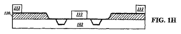
次に、図1Hに示すように、フォトレジストなどの追加マスキング層132が、基板102に施される。フォトレジスト132は、結果として得られるばね接点要素のための望ましい長さおよび幅を画定する型を効果的に形成する開口部を画定するように、パターニングされる。
Next, as shown in FIG. 1H, an
次に、弾性接触構造体140は、弾性接点を形成するために、図1Iに示すようにフォトレジストエリア132間に金属層を施すことによって形成される。フォトレジストエリア132間に堆積される比較的厚い「構造的」金属層は、前述のように、ニッケルなどの弾性材料の電気めっきなどの適切なプロセスを用いて、剥離層130の上に施される。電気めっきの代替として、化学気相成長法(CVD)、物理気相成長法(PVD)または当該技術分野において利用可能な他の技術などの技術を用いて、弾性接触構造体140を形成する金属を施すことが可能である。
Next, the
弾性接触構造体140を形成するように説明した金属層は、結果として得られるばね接触要素の機械的特徴を制御または支配するように意図されている。弾性接触構造体の強化に追加層を含んでもよいことは、本発明の範囲内にある。たとえば、ニッケルなどの弾性材料を堆積する前に、導電率、低接触抵抗、はんだ付け性および耐腐食性の優れた電気特性のために選択された材料層を堆積してもよい。たとえば金またはロジウム(これらは両方とも、良好な接触材料である)、ニッケルコバルト(ろう付けの良好な材料)がある。一実施形態において、弾性材料を堆積する前に、金、アルミニウム、パラジウムコバルトなど、ワイヤボンディングに適した材料が施される。
The metal layer described to form the
図1Jに示すように、接触構造体140およびフォトレジスト材料132は、一旦形成されると、任意に、平坦にラッピング(LAPPING)できる。ばね動作がばね接点の厚さの関数であるので、ラッピングによって、ばね定数のより正確な制御が可能になる。接触構造体140は、研削、化学機械研磨(CMP)、フライス削り、または平坦化に用いられる他の適切なプロセスによって、平坦化できる。図示の細長い弾性接触構造体140には単一の屈曲領域が含まれているが、前に参照した米国特許第6,482,013号明細書に説明されているように、多数の屈曲部を含んでもよい。
As shown in FIG. 1J,
図1Kに示す次のステップにおいて、フォトレジスト材料132が剥がされ、ばね接点140の端部が露出される。図1Lに示すように、露出したブランケットスパッタ金属130がさらに除去され、弾性接点140の下のスパッタ金属130だけが残される。
In the next step shown in FIG. 1K, the
図1Mに示す次のステップにおいて、エポキシなどの接着剤144が、弾性接点140の端部およびフォトレジスト120の一部の上に施される。当該技術分野において周知のように、接着剤は、さらなる強度のために粒子で満たしてもよい。図1Nに示すさらなるステップにおいて、支持基板150が、エポキシの上に貼付され、エポキシが硬化する。図1Oに示すように、硬化したエポキシは、支持基板150を弾性接点140に接合する。一実施形態において、支持基板150は、ガラスなどの透明材料であり、弾性接点140をスペース変換基板に配置するときに、透明基板を通して見ることによって、弾性接点140の視覚的な整列を可能にする。支持基板150は同様に、重合体もしくはセラミックなどの別の誘電材料、または金属などの導電性材料にすることができる。
In the next step shown in FIG. 1M, an adhesive 144 such as epoxy is applied over the ends of the
一実施形態において、図1Nに示すように、導電性金属材料152を、支持基板150の1つまたは複数の領域に施して、弾性接点140の下にある接地プレートを形成することができる。接地プレート152は、弾性接点140の下で容量層を提供して、より良好なインピーダンス整合を提供する役目をする。接触要素140の下にある1つまたは複数の接地プレート領域152のサイジングは、図1Nにおけるギャップ幅「g」のサイジングと同様に、インピーダンス整合のために調節できる。一実施形態において、支持基板150全体は、導電性金属材料から形成でき、接着剤144は、支持基板(または接地プレート)を弾性接点140から電気的に絶縁する非導電性誘電体を形成する。接地プレートはまた、支持基板150の反対側に形成できる。
In one embodiment, as shown in FIG. 1N, a
弾性接点140が、接着剤144によって支持基板に150に貼付され、次のステップにおいて、図1Oに示すように、フォトレジスト材料120が剥がされ、図1Pに示すように、犠牲基板102を分離している残されたブランケットスパッタ金属130が、犠牲基板102と共にエッチングされる。
The
図1A〜図1Pは、支持基板に細長い弾性(ばね)相互接続(接触)要素を作製するための例示的なプロセスを説明している。これは、続いて説明するように、さらに利用可能な「中間」製品と見なすことができる。 1A-1P illustrate an exemplary process for making elongated elastic (spring) interconnect (contact) elements on a support substrate. This can be viewed as a further available “intermediate” product, as will be explained subsequently.
図1A〜図1Pにおいて形成された接触構造体140を備えた支持基板150は、図2に示すように、一実施形態において電気ルーティング線161を含むさらなる基板160に接着または接合される。次に、接触構造体140は、基板160におけるルーティング線161に接続するボンドパッド163に接触するワイヤボンド162によって接続される。一実施形態において、接地プレート領域152は、1つまたは複数のワイヤボンド164によって、基板160を通して設けられた接地接続線165にさらに接続される。基板160が、ワイヤボンドパッド163から、ルーティング線161を通って、基板160の反対面の別のピッチにおける接点へ電気ルーティングを提供するので、基板160は、「スペース変換器」基板を効果的に形成する。スペース変換基板160に取り付けて示しているが、基板160は、その表面にのみルーティング線を備えた基板または「スペース変換」を少しも提供しない、貫通線ビアを備えた基板などの他の形状を取ることができる。基板160は、多層セラミック材料、効果的にPCBを形成する高分子材料、または適していると当業者には考えられるような他の材料から、形成できる。便宜上、支持基板150などの弾性接点支持基板に付着している基板160などの基板のさらなる言及では、「スペース変換基板」と呼ぶ。
The
図3は、スペース変換基板160に取り付けるための別の構成を示すが、この場合には、支持基板151は、ビア172を含むように変更されている。ビア172は、支持基板151の表面上のボンドパッド177から、支持基板151の反対側に設けられたはんだバンプ174へ導電線を提供する。はんだバンプ174は、支持基板151をスペース変換基板160に接続するように働く。代替として、はんだバンプ174に加えて、エポキシまたは当該技術分野において周知のアンダーフィル(図示せず)などの粘着性充填材料を、支持基板151とスペース変換基板160との間にさらに設けて、基板を接続する。はんだバンプ174は、ビア172を、スペース変換基板160内の電気ルーティング線161に接続する。ビア172の反対側端部にはバンプまたはボンドパッド177が含まれるが、これらは次に、ワイヤボンド175によって接触構造体140に接続される。1つまたは複数の追加ビア173を設けて、接地プレート領域152を、スペース変換基板160内の接地線161に接続できる。
FIG. 3 shows another configuration for attachment to the
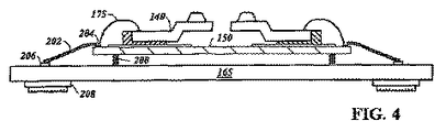
図4は、取り付けのための別の構成を示すが、この場合には、弾性ばね200が、支持基板150とプリント回路基板(PCB)165との間に設けられている。支持構造体150は、弾性ばね200に取り付けられることによって、ウエハ上の部品をテストするための弾性プラットフォームを形成し、弾性性質によって、テストプロービング中に、ウエハまたはその上に形成された部品を損傷する可能性が制限される。弾性ばね200は、図示のような金属コイルばね、弾性接点140と類似の細長いばね、弾性エラストマから作製されたばね構造体もしくはゴムなどのフレキシブル材料、または当該技術分野において周知の他の弾性材料にすることができる。フレキシブル導電接続部202は、PCB165を弾性接点140に接続する。フレキシブル接続部202は、支持構造体150上のパッド204、およびPCB基板165上のソケット206または他のフレキシブル接続部に接合されるように、図4に示されている。フレキシブル接続部202は、超音波圧縮または当該技術分野において周知の他の接合手順を用いて、ボンドパッド204およびソケット206に接続される。ワイヤボンド175は、弾性接点140をボンドパッド204に接続する。スペース変換PCB165(図示せず)内のルーティング線は、ウエハテスタに接続するために、フレキシブル接続部202を、PCB165の反対側のコネクタ208へ接続する。
FIG. 4 shows another configuration for attachment, in which case an
別個のワイヤボンド175を用いずに、弾性接点140が、フレキシブル接続部202によって、PCB基板165上のパッド206に直接接続されるように、図5は、図4の弾性プラットフォーム構成に対する変更を示す。図5の構造は、フレキシブル接続部が弾性接点140にそれほどの量の力をかけない場合、または弾性接点140からPCB基板165へのより短い電気経路を有することによって、より良好な電気特性が得られる場合には、製造を単純化するために有用であり得る。
FIG. 5 shows a modification to the elastic platform configuration of FIG. 4 such that the
図6は、弾性接点140が透明支持基板150に設けられ、かつPCB165に取り付けられた別の構成を示すが、PCB165は、光が透明支持基板150を通過して感光装置をテストできるようにする1つまたは複数の開口部210を有する。基板150は、接着剤144と類似のエポキシなどの接着剤を用いてか、または図4〜図5におけるように弾性プラットフォームを形成する弾性ばねを用いて、PCB165に付着できる。図6の構成は、ウエハ212の上方に設けて示したが、弾性接点140は、ウエハ上のICをテストするために、ウエハ212上のプロービングパッド214に対して整列されている。弾性接点140への信号およびそこからの信号は、図4〜図5に示すように、コネクタ208を通ってテスタに供給される。ウエハ212を、電荷結合素子(CCD)、カメラ付携帯電話用画像センサ、または感光性の類似光学部品などの感光装置216と共にさらに示す。レーザまたは発光ダイオードなどの光源218は、テスト構造体の上方に設けて示す。光源218から放射された光は、PCB165における開口部210および透明支持基板150を通して供給され、テストのために、ウエハ212上の感光部品216に信号を供給する。したがって、ウエハ212上の光学および電気部品のテストは、同時に行うことができる。
FIG. 6 shows another configuration in which
図7は、単一DUTにおけるパッドの一構成と接触するように設定された、支持基板150上の弾性接触構造体140の上面図を示す。図7では、図2の断面で示す構成と同様に、ワイヤボンディングが、弾性接触構造体140から、スペース変換基板160上のボンドパッド163へ提供されている。弾性接触構造体140は、(図1D−1に示す貫入部110に形成された)先端部180がDUT接触パッド(図示せず)の上に提供されるように、支持基板150上に配置される。破線はDUTの周辺エリアを示すが、パッドの一構成がDUTの周辺部辺りに配置されている。ワイヤボンド162が、接触構造体140を、スペース変換基板160上の接触パッド163に接続する。さらなるワイヤボンド164が、支持基板150の表面における接地プレートを、スペース変換基板160上の接地線接触パッド178に接続する。接地に至るワイヤボンド164は、良好な信号忠実度のために、信号線のすぐ近くに配置される。単一の接地線164だけを示すが、信号忠実度を改善するために追加の線路を設けることができる。図7では、接地プレートが、支持基板150の表面全体にわたって設けられていると仮定されているが、しかし1つまたは複数の接触構造体140の下にある個別接地プレート領域を代替として用いてもよい。非導電性接着剤144が、接地プレート領域を接触構造体140から分離する。一実施形態において、接触パッド163および178は、図2に示す線路の配置と同様に、スペース変換器160の内部線路に接続されていると仮定されている。
FIG. 7 shows a top view of the
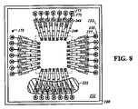
図8は、図3の配置と同様に、スペース変換基板166に接続するためのパッドおよびビアを代替として有する支持基板151上の弾性接触構造体140の上面図を示す。信号ビアは、基板151のパッド177で終端する。次に、支持基板151における接地プレート領域152は、ビアに接続する信号パッド177を電気的に絶縁するために開口部153を有する。接地プレート領域152は、信号パッド177を囲んで示されているが、代替として、信号パッド177は、支持基板151における接地プレート領域の外に設けることが可能である。次に、接地プレート領域152は、ビア173によって、スペース変換基板160における接地線に直接接続される。接触構造体140は、非導電性接着剤144によって、接地プレート152から電気的に絶縁される。弾性接触構造体140は、ワイヤボンド175によって、ボンドパッド177に接続される。前述のように、接地プレート領域152(または、別個の接地プレートが各接点の下にある場合には領域)のサイズは、ワイヤボンド175および接触構造体140を通して、結果として生じるインピーダンスを制御するように調節できる。一実施形態において、接着剤222は、多くのプローブにわたって連続的なビーズに分配できる。前に言及したように、接着剤222は、曲げ強さを改善するか、または支持基板151からのプローブ140の剥離を防ぐために提供される。接着剤222の例には、エポキシ樹脂、充填エポキシ、シアン酸エステル、BCB、または当該技術分野で認められた接着性を備えた他の材料が含まれる。
FIG. 8 shows a top view of the
図8に示すように弾性接点140をビア上のパッド177へ直接ワイヤボンディングする代わりとして、図9に示すように、ある長さのトレース181を加えることができる。トレース181の長さによって、ボンドワイヤ175はビア172に接続される。トレース181の長さおよびサイズは、インピーダンス整合を改善するために調節できる。トレース181には、インピーダンス整合を提供するサイズの薄膜抵抗器をさらに含むことができる。より高いインピーダンスは、トレース181を構成する導電線のサイズを単に調節するのとは対照的に、薄膜抵抗器をトレース181に設けることで達成できる。薄膜抵抗器は、導電線の直列素子として、または終端部として働くことが可能である。トレース181にはまた、高周波コンデンサを含むことができる。コンデンサは、別個の直列素子として働くことか、または接地へのバイパスを提供することが可能である。図9の代替を図10に示すが、そこでは、ビアを用いるのではなく、トレース181がボンドパッド接続部を提供する。図10に示すように、第1のボンドワイヤ194が、弾性接点140をトレース181の第1の端部に接続する一方で、別のボンドワイヤ196が、トレース181の第2の端部をスペース変換基板160上のボンドパッド198に接続する。スペース変換基板160における内部ルーティング線197が、ボンドパッド198を基板160の反対側に接続する。
As an alternative to wire bonding the
図11は、支持基板150上の弾性接触構造体140の配置のために図7および8に示した構成に対する代替構成の上面図を示す。図示のように、弾性接触構造体140は、先端部180が、DUTの中心線に沿って配置されたパッドの上に配列されるように、再配置される。DUTの周囲は、破線によって示されている。図7には示していないが、ワイヤボンディングおよび接地プレートは、前述のように提供できる。
FIG. 11 shows a top view of an alternative configuration to the configuration shown in FIGS. 7 and 8 for the placement of the
図12は、弾性接触構造体を自身の上に形成した基板150の上面図を示し、製造歩留まりを改善するためにどのように基板150を製造し、次にダイシングすることができるかを例示する。図示の構成には、図7および8に示すように自身の周辺近くに接点を有するDUT上のパッドと接触するように構成されている弾性ばね接点群が含まれる。ばね接点の26の群が、ウエハ形状を有する支持基板150に形成されて示されている。線は、ばね接点群のうちの個別ばね接点の境界を示す。切断は、支持基板150を26の個別DUTテスト構造体へダイシングするための線に沿って行うことができる。個別支持基板タイルは、ダイシングの前または後にテストすることができ、テストによって、タイルが機能できると証明された場合には、前述のように、タイルを、スペース変換基板に付着できる。支持基板150をダイシングして個別タイルを形成し、機能しないタイルを廃棄することによって、製造歩留まりを改善できる。
FIG. 12 shows a top view of a
図12に示す線に沿ってダイシングする代わりとして、ダイシングは、より大きな破線190で示すように、弾性接点群のうちの2つ以上を一緒にして実行することができる。したがって、互いに対して接点群の正確な整列を維持できる一方で、4つの群のいくつかを、それらが機能しない場合には廃棄することで、製造歩留まりの増加がやはり提供される。 As an alternative to dicing along the line shown in FIG. 12, dicing can be performed with two or more of the elastic contact groups together, as shown by the larger dashed line 190. Thus, while maintaining an exact alignment of the contact groups relative to each other, discarding some of the four groups if they do not work still provides an increase in manufacturing yield.
図13は、プローブカードの構成要素の断面図を示すが、テストシステムコントローラに接続するためのコネクタ203を含むPCB165に接続するために、図4〜図5で用いられる弾性ばね200の代替として、スペース変換基板160の柔軟な取り付けを例示する。スペース変換基板160は、図2〜図3に示すようにかまたは図6と類似の光学的接続を可能にする開口部を備えたシステムとして、図13に示すシステムを用いて柔軟に取り付けるように構成できる。図7〜図11に示す他の構成も同様に、図13に示すように柔軟に取り付けできる。
FIG. 13 shows a cross-sectional view of the probe card components, but as an alternative to the
図13のプローブカードは、ウエハに直接接触するプローブ140に対して電気経路および機械的支持の両方を提供するように構成して示す。図13には、図2に示すように構成されたスペース変換器160が含まれる。プローブカードの電気経路は、プリント回路基板(PCB)165と同様にスペース変換器160、およびインタポーザ232を通して設けられている。テストシステムコントローラのためのテストデータは、PCB165の周辺部辺りに接続されたポゴピンまたはゼロ挿入力(ZIF)コネクタ203を通して供給される。チャネル伝送線240は、PCB165において水平にテスタインタフェースコネクタ(ポゴまたはZIF)203からPCB165上の接触パッドへ信号を分配し、スペース変換器160上のパッドのルーティングピッチと一致させる。インタポーザ232には、ばねプローブ電気接点44が両側に配置された基板42が含まれる。インタポーザ232は、PCB165上の個別パッドを、スペース変換器160にランドグリッドアレイ(LGA)を形成しているパッドへ電気的に接続する。LGAパッド接続部は、典型的には規則的な多列パターンで配置される。スペース変換器160の基板45における伝送線246は、LGAから、アレイに構成されたばねプローブ140へ、信号線を分配または「スペース変換」する。埋め込み回路、プローブおよびLGAを備えたスペース変換器160は、プローブヘッドと呼ばれる。
The probe card of FIG. 13 is shown configured to provide both electrical path and mechanical support for the
電気部品の機械的支持は、バックプレート250、ブラケット252、フレーム254、板ばね256およびレベリングピン262によって提供される。バックプレート250がPCB165の一つの側に設けられる一方で、ブラケット252は、もう一方の側に設けられてねじ259で装着される。板ばね256は、ねじ258によってブラケット252に装着される。板ばね256は延びて、フレーム254をブラケット252の内壁内に可動に保持する。次に、フレーム254は、スペース変換器160を支持するための水平拡張部260を、その内壁内に含む。フレーム254は、プローブヘッドを囲んで、横移動を制限するようにブラケット252に対して精密許容誤差を維持する。
Mechanical support for the electrical components is provided by
レベリングピン262は、電気部品の機械的支持を完成させ、スペース変換器234の水平化を提供する。レベリングピン262を調節して、真鍮球体266が、スペース変換器160との点接触を提供するようにする。球体266は、スペース変換器160におけるLGAの周囲の外側で接触し、電気部品からの絶縁を維持する。基板の水平化は、レベリングピンと呼ばれる前進ねじ262を用いることを介して、これらの球体を正確に調節することによって達成される。レベリングピン262は、スペース変換器160を水平にするように調節可能であり、全てのプローブ140がウエハと接触することを保証する。レベリングピン262は、バックプレート250において支持部265を通して回される。球体266がスペース変換器160と接したままになるように、レベリングピンねじ262の動きは、板ばね256によって対抗される。板ばね256は、インタポーザ232よりずっと強くなるように設計され、その結果、レベリングねじ262の上昇および下降は、板ばね256によって対抗され、インタポーザ232のばね242および244は、スペース変換器160がPCB165に対して移動するときに、電気接触が、スペース変換器160間に維持されるように保証するためにのみ働く。
Leveling pins 262 complete the mechanical support of the electrical components and provide leveling of the
上記で本発明を詳細に説明したが、それは、単に、どのように本発明を作製し用いるかを当業者に教示するためのものである。本発明の範囲が特許請求の範囲によって定義されているように、多くの追加的な変更が本発明の範囲に包含される。 Although the present invention has been described in detail above, it is merely intended to teach those skilled in the art how to make and use the invention. Many additional modifications are encompassed within the scope of the invention, as the scope of the invention is defined by the claims.
Claims (34)
前記支持基板を前記追加基板に接続する弾性要素と、
前記ばね接触要素を前記ボンドパッドに接続するフレキシブル導電要素と、
をさらに含む、請求項1に記載の装置。 An additional substrate having a bond pad;
An elastic element connecting the support substrate to the additional substrate;
A flexible conductive element connecting the spring contact element to the bond pad;
The apparatus of claim 1, further comprising:
前記支持基板を前記追加基板に接続する弾性要素と、
前記ばね接触要素を前記支持基板上のボンドパッドに接続するフレキシブル導電要素と、
前記追加基板の前記ボンドパッドを前記支持基板上のボンドパッドに接続するワイヤボンドと、
をさらに含む、請求項1に記載の装置。 An additional substrate having a bond pad;
An elastic element connecting the support substrate to the additional substrate;
A flexible conductive element connecting the spring contact element to a bond pad on the support substrate;
Wire bonds connecting the bond pads of the additional substrate to bond pads on the support substrate;
The apparatus of claim 1, further comprising:
前記ばね接触要素を前記ボンドパッドに接続するワイヤボンドと、
をさらに含む、請求項1に記載の装置。 An additional substrate having a bond pad, the additional substrate having the support substrate attached thereto;
A wire bond connecting the spring contact element to the bond pad;
The apparatus of claim 1, further comprising:
前記支持基板に設けられたトレースであって、前記支持基板が前記追加基板上の電気接点を前記トレースに接続する信号ビアを含む、トレースと、
前記ばね接触要素を前記トレースに接続するワイヤボンドと、
をさらに含む、請求項1に記載の装置。 An additional substrate to which the support substrate is attached;
A trace provided on the support substrate, wherein the support substrate includes signal vias connecting electrical contacts on the additional substrate to the trace; and
A wire bond connecting the spring contact element to the trace;
The apparatus of claim 1, further comprising:
前記支持基板に設けられたトレースと、
前記ばね接触要素を前記トレースの第1の端部に接続する第1のワイヤボンドと、
前記トレースを前記ボンドパッドに接続する第2のワイヤボンドと、
をさらに含む、請求項1に記載の装置。 An additional substrate having a bond pad, the additional substrate having the support substrate attached thereto;
Traces provided on the support substrate;
A first wire bond connecting the spring contact element to the first end of the trace;
A second wire bond connecting the trace to the bond pad;
The apparatus of claim 1, further comprising:
前記基板を別個のユニットにダイシングすること、
を含む方法。 Forming multiple probe leads on a single substrate; and
Dicing the substrate into separate units;
Including methods.
犠牲基板を設けること、
前記犠牲基板に、前記接触要素のための接触先端部を形成するための貫入部を形成すること、
フォトレジストの第1の層を施し、かつ前記フォトレジストをパターニングして、前記貫入部および前記貫入部に隣接する前記犠牲基板の領域の上に開口部を形成すること、
前記露出した犠牲基板上の導電層および第2のフォトレジスト層を施すこと、
フォトレジストの第2の層を施しかつパターニングして、前記第1のフォトレジスト層の一部、および前記貫入部とは別個の前記犠牲基板上に開口部を形成すること、
フォトレジストの前記第2の層の領域間に形成された開口部に弾性金属材料を施し、フォトレジストの前記第2の層を除去すること、
前記貫入部とは別個の、前記接触要素の一部の上に接着剤を施すこと、
前記支持基板を前記接着剤に付着させること、
前記第1のフォトレジスト材料を除去すること、および、
前記犠牲基板を除去すること、
を含む方法。 A method of forming a contact element on a support substrate, comprising:
Providing a sacrificial substrate,
Forming a penetration in the sacrificial substrate to form a contact tip for the contact element;
Applying a first layer of photoresist and patterning the photoresist to form an opening over the penetration and a region of the sacrificial substrate adjacent to the penetration;
Applying a conductive layer and a second photoresist layer on the exposed sacrificial substrate;
Applying and patterning a second layer of photoresist to form an opening on a portion of the first photoresist layer and on the sacrificial substrate separate from the penetration;
Applying an elastic metal material to an opening formed between regions of the second layer of photoresist and removing the second layer of photoresist;
Applying an adhesive on a portion of the contact element that is separate from the penetration;
Attaching the support substrate to the adhesive;
Removing the first photoresist material; and
Removing the sacrificial substrate;
Including methods.
前記接触要素を前記ボンドパッドの1つにワイヤボンディングすること、
をさらに含む、請求項31に記載の方法。 Attaching the support substrate to a space conversion substrate having bond pads attached to routing lines within the support substrate; and
Wire bonding the contact element to one of the bond pads;
32. The method of claim 31, further comprising:
Applications Claiming Priority (2)
| Application Number | Priority Date | Filing Date | Title |
|---|---|---|---|
| US10/922,486 US7459795B2 (en) | 2004-08-19 | 2004-08-19 | Method to build a wirebond probe card in a many at a time fashion |
| PCT/US2005/029581 WO2006023741A2 (en) | 2004-08-19 | 2005-08-19 | Method to build a wirebond probe card in a many at a time fashion |
Publications (2)
| Publication Number | Publication Date |
|---|---|
| JP2008510966A true JP2008510966A (en) | 2008-04-10 |
| JP2008510966A5 JP2008510966A5 (en) | 2008-10-09 |
Family
ID=35910115
Family Applications (1)
| Application Number | Title | Priority Date | Filing Date |
|---|---|---|---|
| JP2007528044A Pending JP2008510966A (en) | 2004-08-19 | 2005-08-19 | How to make wire bond probe cards in multiple ways at once |
Country Status (7)
| Country | Link |
|---|---|
| US (2) | US7459795B2 (en) |
| EP (1) | EP1779128A2 (en) |
| JP (1) | JP2008510966A (en) |
| KR (2) | KR20070053743A (en) |
| CN (1) | CN101292337B (en) |
| TW (1) | TWI410648B (en) |
| WO (1) | WO2006023741A2 (en) |
Cited By (6)
| Publication number | Priority date | Publication date | Assignee | Title |
|---|---|---|---|---|
| JP2007101506A (en) * | 2005-10-07 | 2007-04-19 | Japan Electronic Materials Corp | Method of manufacturing probe card |
| JP2008281564A (en) * | 2007-05-11 | 2008-11-20 | Amst Co Ltd | Probe card and its manufacturing method |
| JP2012242196A (en) * | 2011-05-18 | 2012-12-10 | Mitsubishi Electric Corp | High-frequency characteristics measuring device |
| JP2016538718A (en) * | 2013-11-19 | 2016-12-08 | テラダイン、 インコーポレイテッド | Interconnects for transmitting signals between devices and testers |
| CN111366839A (en) * | 2020-03-28 | 2020-07-03 | 深圳中科系统集成技术有限公司 | Probe adapter plate for wafer test and manufacturing method thereof |
| JP2022070228A (en) * | 2020-10-26 | 2022-05-12 | プロ-2000・カンパニー・リミテッド | Probe card for testing wafer |
Families Citing this family (69)
| Publication number | Priority date | Publication date | Assignee | Title |
|---|---|---|---|---|
| US8033838B2 (en) | 1996-02-21 | 2011-10-11 | Formfactor, Inc. | Microelectronic contact structure |
| US9097740B2 (en) | 2004-05-21 | 2015-08-04 | Formfactor, Inc. | Layered probes with core |
| US9476911B2 (en) | 2004-05-21 | 2016-10-25 | Microprobe, Inc. | Probes with high current carrying capability and laser machining methods |
| US8988091B2 (en) | 2004-05-21 | 2015-03-24 | Microprobe, Inc. | Multiple contact probes |
| USRE43503E1 (en) | 2006-06-29 | 2012-07-10 | Microprobe, Inc. | Probe skates for electrical testing of convex pad topologies |
| US7759949B2 (en) | 2004-05-21 | 2010-07-20 | Microprobe, Inc. | Probes with self-cleaning blunt skates for contacting conductive pads |
| US7459795B2 (en) | 2004-08-19 | 2008-12-02 | Formfactor, Inc. | Method to build a wirebond probe card in a many at a time fashion |
| JP4651359B2 (en) * | 2004-10-29 | 2011-03-16 | ルネサスエレクトロニクス株式会社 | Semiconductor device and manufacturing method thereof |
| KR20080002793A (en) * | 2005-03-01 | 2008-01-04 | 에스브이 프로브 피티이 엘티디 | Probe card with stacked substrate |
| TWI273246B (en) * | 2005-05-25 | 2007-02-11 | Chipmos Technologies Inc | Elastic probe pins in row and method for fabricating the same |
| CA2612473A1 (en) * | 2005-06-17 | 2006-12-21 | Shell Internationale Research Maatschappij B.V. | Modified sulphur and product comprising modified sulphur as binder |
| US7649367B2 (en) | 2005-12-07 | 2010-01-19 | Microprobe, Inc. | Low profile probe having improved mechanical scrub and reduced contact inductance |
| JP4654897B2 (en) | 2005-12-09 | 2011-03-23 | イビデン株式会社 | Method for manufacturing printed wiring board having component mounting pins |
| JP2007165383A (en) | 2005-12-09 | 2007-06-28 | Ibiden Co Ltd | Printed wiring board having component mounting pin formed thereon |
| JP4848752B2 (en) * | 2005-12-09 | 2011-12-28 | イビデン株式会社 | Printed wiring board having component mounting pins and electronic device using the same |
| TWI271525B (en) * | 2006-01-17 | 2007-01-21 | Chipmos Technologies Inc | Probe head with vertical probes, method for manufacturing the probe head, and probe card using the probe head |
| JP2007248064A (en) * | 2006-03-13 | 2007-09-27 | Japan Electronic Materials Corp | Semiconductor element inspection device |
| US7312617B2 (en) * | 2006-03-20 | 2007-12-25 | Microprobe, Inc. | Space transformers employing wire bonds for interconnections with fine pitch contacts |
| US7732233B2 (en) * | 2006-07-24 | 2010-06-08 | Touch Micro-System Technology Corp. | Method for making light emitting diode chip package |
| US20090273005A1 (en) * | 2006-07-24 | 2009-11-05 | Hung-Yi Lin | Opto-electronic package structure having silicon-substrate and method of forming the same |
| TWI320237B (en) * | 2006-07-24 | 2010-02-01 | Si-substrate and structure of opto-electronic package having the same | |
| US20090273004A1 (en) * | 2006-07-24 | 2009-11-05 | Hung-Yi Lin | Chip package structure and method of making the same |
| US20080044623A1 (en) * | 2006-08-21 | 2008-02-21 | John Caldwell | Probe card for testing imaging devices, and methods of fabricating same |
| US7836587B2 (en) * | 2006-09-21 | 2010-11-23 | Formfactor, Inc. | Method of repairing a contactor apparatus |
| US8907689B2 (en) | 2006-10-11 | 2014-12-09 | Microprobe, Inc. | Probe retention arrangement |
| CN101034947B (en) * | 2007-04-06 | 2011-04-20 | 中兴通讯股份有限公司 | Mobile phone thimble-type RF calibration clamp |
| US7514948B2 (en) | 2007-04-10 | 2009-04-07 | Microprobe, Inc. | Vertical probe array arranged to provide space transformation |
| US20080286633A1 (en) * | 2007-05-17 | 2008-11-20 | Kathleen Ritter Olenick | Circuit testing device for solid oxide fuel cell |
| CN101889338B (en) * | 2007-10-08 | 2012-10-24 | Amst株式会社 | Method for wafer test and probe card for the same |
| US8723546B2 (en) | 2007-10-19 | 2014-05-13 | Microprobe, Inc. | Vertical guided layered probe |
| MY144280A (en) * | 2007-11-20 | 2011-08-29 | Mimos Berhad | Mems based probe card and a method of testing semiconductor ion sensor using the same |
| US7692436B2 (en) * | 2008-03-20 | 2010-04-06 | Touchdown Technologies, Inc. | Probe card substrate with bonded via |
| US8230593B2 (en) | 2008-05-29 | 2012-07-31 | Microprobe, Inc. | Probe bonding method having improved control of bonding material |
| US20100126764A1 (en) * | 2008-11-24 | 2010-05-27 | Seagate Technology, Llc | die ground lead |
| US8115504B2 (en) * | 2008-12-08 | 2012-02-14 | Formfactor, Inc. | Microspring array having reduced pitch contact elements |
| JP2011196934A (en) * | 2010-03-23 | 2011-10-06 | Hitachi Ltd | Testing method and interposer used for the same |
| US8154119B2 (en) | 2010-03-31 | 2012-04-10 | Toyota Motor Engineering & Manufacturing North America, Inc. | Compliant spring interposer for wafer level three dimensional (3D) integration and method of manufacturing |
| ES2811552T3 (en) * | 2010-10-22 | 2021-03-12 | C Miethke Gmbh&Co Kg | Implant for intrabody pressure measurement with telemetric transmission of the measurement value |
| US10675451B2 (en) | 2010-10-22 | 2020-06-09 | Christoph Miethke Gmbh & Co Kg | Hydrocephalus shunt arrangement and components thereof for draining cerebrospinal fluid in a patient having hydrocephalus |
| CN102586842A (en) * | 2011-01-06 | 2012-07-18 | 刘江涛 | Manufacturing method for composite reinforcement spring |
| JP5681213B2 (en) * | 2011-01-16 | 2015-03-04 | 日本電子材料株式会社 | Probe card and manufacturing method thereof |
| JP5777997B2 (en) * | 2011-03-07 | 2015-09-16 | 日本特殊陶業株式会社 | Wiring board for electronic component inspection apparatus and manufacturing method thereof |
| JP5798435B2 (en) | 2011-03-07 | 2015-10-21 | 日本特殊陶業株式会社 | Wiring board for electronic component inspection apparatus and manufacturing method thereof |
| KR101241937B1 (en) * | 2011-04-07 | 2013-03-13 | (주)미르시스템 | Method for testing the FPCB using probe sheet |
| US8803001B2 (en) | 2011-06-21 | 2014-08-12 | Toyota Motor Engineering & Manufacturing North America, Inc. | Bonding area design for transient liquid phase bonding process |
| US9024651B2 (en) * | 2011-07-06 | 2015-05-05 | Celadon Systems, Inc. | Test apparatus having a probe card and connector mechanism |
| US8994390B2 (en) | 2011-07-06 | 2015-03-31 | Celadon Systems, Inc. | Test systems with a probe apparatus and index mechanism |
| TWI428608B (en) * | 2011-09-16 | 2014-03-01 | Mpi Corp | Probing device and manufacturing method thereof |
| US10859602B2 (en) | 2012-03-07 | 2020-12-08 | Advantest Corporation | Transferring electronic probe assemblies to space transformers |
| KR101378012B1 (en) | 2012-03-14 | 2014-03-24 | 삼성전자주식회사 | Multi array type ultrasonic probe apparatus and method for fabricating multi array type ultrasonic probe apparatus |
| US10058951B2 (en) | 2012-04-17 | 2018-08-28 | Toyota Motor Engineering & Manufacturing North America, Inc. | Alloy formation control of transient liquid phase bonding |
| US9044822B2 (en) | 2012-04-17 | 2015-06-02 | Toyota Motor Engineering & Manufacturing North America, Inc. | Transient liquid phase bonding process for double sided power modules |
| TWI454710B (en) * | 2012-09-19 | 2014-10-01 | Mpi Corp | Probe card and its manufacturing method |
| CN103869109B (en) * | 2012-12-12 | 2017-10-10 | 华邦电子股份有限公司 | Probe card and its welding method |
| TWI503554B (en) * | 2013-06-04 | 2015-10-11 | Mpi Corp | Probe card and manufacturing method thereof |
| TWI541959B (en) * | 2013-10-22 | 2016-07-11 | And a space converter for a wafer carrier for a wafer having a long strip contact is used And its manufacturing method | |
| US9372205B2 (en) * | 2014-01-15 | 2016-06-21 | Taiwan Semiconductor Manufacturing Co., Ltd. | Universal probe card PCB design |
| CN105390517B (en) * | 2015-11-17 | 2023-10-27 | 格科微电子(上海)有限公司 | Testing method and testing device for camera module |
| US10120020B2 (en) | 2016-06-16 | 2018-11-06 | Formfactor Beaverton, Inc. | Probe head assemblies and probe systems for testing integrated circuit devices |
| WO2018035054A1 (en) * | 2016-08-16 | 2018-02-22 | Translarity, Inc. | Space transformers for probe cards, and associated systems and methods |
| IT201600124017A1 (en) * | 2016-12-06 | 2018-06-06 | Technoprobe Spa | Measurement head of an electronic device test device and its manufacturing method |
| WO2018182719A1 (en) * | 2017-03-31 | 2018-10-04 | Intel Corporation | Ultra low-cost, low leadtime, and high density space transformer for fine pitch applications |
| EP3704496A4 (en) * | 2017-10-31 | 2021-08-11 | FormFactor, Inc. | Mems probe card assembly having decoupled electrical and mechanical probe connections |
| KR102447833B1 (en) * | 2018-02-09 | 2022-09-27 | 주성엔지니어링(주) | Electric power interface |
| TWI759594B (en) * | 2018-10-12 | 2022-04-01 | 旺矽科技股份有限公司 | Probe module with microelectromechanical probe and its manufacturing method |
| JP7302011B2 (en) * | 2019-04-26 | 2023-07-03 | フォームファクター, インコーポレイテッド | Probes on carrier structures for vertical probe arrays |
| KR102164020B1 (en) * | 2019-11-27 | 2020-10-13 | 화인인스트루먼트 (주) | Probe head manufacturing method of the probe card |
| US11243230B2 (en) | 2019-12-30 | 2022-02-08 | Juniper Networks, Inc. | Compact opto-electric probe |
| TWI755919B (en) * | 2020-11-03 | 2022-02-21 | 中華精測科技股份有限公司 | Board-like connector, dual-ring bridge of board-like connector, and wafer testing assembly |
Citations (7)
| Publication number | Priority date | Publication date | Assignee | Title |
|---|---|---|---|---|
| JPH06140484A (en) * | 1992-10-28 | 1994-05-20 | Nippon Telegr & Teleph Corp <Ntt> | Probe card |
| JP2000174078A (en) * | 1998-12-08 | 2000-06-23 | Advantest Corp | Probe card and its manufacturing method |
| JP2002139517A (en) * | 1994-06-03 | 2002-05-17 | Hitachi Ltd | Manufacturing method of semiconductor device |
| JP2003202350A (en) * | 2001-12-28 | 2003-07-18 | Tokyo Cathode Laboratory Co Ltd | Probe and probe unit for probe card, probe card and method of manufacturing the same |
| JP2003232809A (en) * | 1996-05-17 | 2003-08-22 | Formfactor Inc | Microelectronic contact structure and its manufacturing method |
| WO2003071289A1 (en) * | 2002-02-19 | 2003-08-28 | Advantest Corporation | Contact structure having silicon finger contactor |
| JP2004501517A (en) * | 2000-06-20 | 2004-01-15 | ナノネクサス インコーポレイテッド | System for testing and packaging integrated circuits |
Family Cites Families (27)
| Publication number | Priority date | Publication date | Assignee | Title |
|---|---|---|---|---|
| US5476211A (en) | 1993-11-16 | 1995-12-19 | Form Factor, Inc. | Method of manufacturing electrical contacts, using a sacrificial member |
| JPS62165944A (en) | 1986-01-17 | 1987-07-22 | Fujitsu Ltd | Wire connecting method |
| JP2718785B2 (en) * | 1988-10-25 | 1998-02-25 | 日立化成工業株式会社 | Naphthalocyanine derivative, method for producing the same, optical recording medium using the same, and method for producing the optical recording medium |
| US6482013B2 (en) | 1993-11-16 | 2002-11-19 | Formfactor, Inc. | Microelectronic spring contact element and electronic component having a plurality of spring contact elements |
| US5974662A (en) | 1993-11-16 | 1999-11-02 | Formfactor, Inc. | Method of planarizing tips of probe elements of a probe card assembly |
| US7064566B2 (en) | 1993-11-16 | 2006-06-20 | Formfactor, Inc. | Probe card assembly and kit |
| US6023103A (en) * | 1994-11-15 | 2000-02-08 | Formfactor, Inc. | Chip-scale carrier for semiconductor devices including mounted spring contacts |
| US5806181A (en) * | 1993-11-16 | 1998-09-15 | Formfactor, Inc. | Contact carriers (tiles) for populating larger substrates with spring contacts |
| US5613861A (en) * | 1995-06-07 | 1997-03-25 | Xerox Corporation | Photolithographically patterned spring contact |
| US6690185B1 (en) * | 1997-01-15 | 2004-02-10 | Formfactor, Inc. | Large contactor with multiple, aligned contactor units |
| US6215196B1 (en) * | 1997-06-30 | 2001-04-10 | Formfactor, Inc. | Electronic component with terminals and spring contact elements extending from areas which are remote from the terminals |
| US5944537A (en) * | 1997-12-15 | 1999-08-31 | Xerox Corporation | Photolithographically patterned spring contact and apparatus and methods for electrically contacting devices |
| JPH11233216A (en) * | 1998-02-16 | 1999-08-27 | Nippon Denki Factory Engineering Kk | Ic socket for test |
| US6268015B1 (en) * | 1998-12-02 | 2001-07-31 | Formfactor | Method of making and using lithographic contact springs |
| US6917525B2 (en) * | 2001-11-27 | 2005-07-12 | Nanonexus, Inc. | Construction structures and manufacturing processes for probe card assemblies and packages having wafer level springs |
| US7215131B1 (en) * | 1999-06-07 | 2007-05-08 | Formfactor, Inc. | Segmented contactor |
| US6939474B2 (en) * | 1999-07-30 | 2005-09-06 | Formfactor, Inc. | Method for forming microelectronic spring structures on a substrate |
| US6432747B1 (en) | 2000-07-05 | 2002-08-13 | Trw Inc. | Repair method for broken or missing microcircuit package terminal lead |
| US6512183B2 (en) | 2000-10-10 | 2003-01-28 | Matsushita Electric Industrial Co., Ltd. | Electronic component mounted member and repair method thereof |
| JP4527267B2 (en) * | 2000-11-13 | 2010-08-18 | 東京エレクトロン株式会社 | Contactor manufacturing method |
| JP3584219B2 (en) * | 2001-06-28 | 2004-11-04 | 財団法人工業技術研究院 | Method of manufacturing probe card and probe card |
| US6777319B2 (en) | 2001-12-19 | 2004-08-17 | Formfactor, Inc. | Microelectronic spring contact repair |
| JP2005517192A (en) * | 2002-02-05 | 2005-06-09 | ファイコム・コーポレーション | Manufacturing method of electrical contact body for inspection of electronic device and electrical contact body using the same |
| US7047638B2 (en) | 2002-07-24 | 2006-05-23 | Formfactor, Inc | Method of making microelectronic spring contact array |
| US7459795B2 (en) | 2004-08-19 | 2008-12-02 | Formfactor, Inc. | Method to build a wirebond probe card in a many at a time fashion |
| JP2006344653A (en) * | 2005-06-07 | 2006-12-21 | Toshiba Corp | Magnetic random access memory |
| US7836587B2 (en) * | 2006-09-21 | 2010-11-23 | Formfactor, Inc. | Method of repairing a contactor apparatus |
-
2004
- 2004-08-19 US US10/922,486 patent/US7459795B2/en not_active Expired - Fee Related
-
2005
- 2005-08-19 WO PCT/US2005/029581 patent/WO2006023741A2/en active Application Filing
- 2005-08-19 EP EP05789219A patent/EP1779128A2/en not_active Withdrawn
- 2005-08-19 KR KR1020077005488A patent/KR20070053743A/en not_active Application Discontinuation
- 2005-08-19 KR KR1020127024506A patent/KR101293348B1/en not_active IP Right Cessation
- 2005-08-19 JP JP2007528044A patent/JP2008510966A/en active Pending
- 2005-08-19 TW TW094128418A patent/TWI410648B/en not_active IP Right Cessation
- 2005-08-19 CN CN2005800283762A patent/CN101292337B/en not_active Expired - Fee Related
-
2008
- 2008-12-02 US US12/326,486 patent/US7884006B2/en not_active Expired - Fee Related
Patent Citations (7)
| Publication number | Priority date | Publication date | Assignee | Title |
|---|---|---|---|---|
| JPH06140484A (en) * | 1992-10-28 | 1994-05-20 | Nippon Telegr & Teleph Corp <Ntt> | Probe card |
| JP2002139517A (en) * | 1994-06-03 | 2002-05-17 | Hitachi Ltd | Manufacturing method of semiconductor device |
| JP2003232809A (en) * | 1996-05-17 | 2003-08-22 | Formfactor Inc | Microelectronic contact structure and its manufacturing method |
| JP2000174078A (en) * | 1998-12-08 | 2000-06-23 | Advantest Corp | Probe card and its manufacturing method |
| JP2004501517A (en) * | 2000-06-20 | 2004-01-15 | ナノネクサス インコーポレイテッド | System for testing and packaging integrated circuits |
| JP2003202350A (en) * | 2001-12-28 | 2003-07-18 | Tokyo Cathode Laboratory Co Ltd | Probe and probe unit for probe card, probe card and method of manufacturing the same |
| WO2003071289A1 (en) * | 2002-02-19 | 2003-08-28 | Advantest Corporation | Contact structure having silicon finger contactor |
Cited By (9)
| Publication number | Priority date | Publication date | Assignee | Title |
|---|---|---|---|---|
| JP2007101506A (en) * | 2005-10-07 | 2007-04-19 | Japan Electronic Materials Corp | Method of manufacturing probe card |
| JP4711800B2 (en) * | 2005-10-07 | 2011-06-29 | 日本電子材料株式会社 | Probe card manufacturing method |
| JP2008281564A (en) * | 2007-05-11 | 2008-11-20 | Amst Co Ltd | Probe card and its manufacturing method |
| JP2012242196A (en) * | 2011-05-18 | 2012-12-10 | Mitsubishi Electric Corp | High-frequency characteristics measuring device |
| JP2016538718A (en) * | 2013-11-19 | 2016-12-08 | テラダイン、 インコーポレイテッド | Interconnects for transmitting signals between devices and testers |
| CN111366839A (en) * | 2020-03-28 | 2020-07-03 | 深圳中科系统集成技术有限公司 | Probe adapter plate for wafer test and manufacturing method thereof |
| CN111366839B (en) * | 2020-03-28 | 2022-04-12 | 深圳中科系统集成技术有限公司 | Probe adapter plate for wafer test and manufacturing method thereof |
| JP2022070228A (en) * | 2020-10-26 | 2022-05-12 | プロ-2000・カンパニー・リミテッド | Probe card for testing wafer |
| JP7232305B2 (en) | 2020-10-26 | 2023-03-02 | プロ-2000・カンパニー・リミテッド | Wafer test probe card |
Also Published As
| Publication number | Publication date |
|---|---|
| US7459795B2 (en) | 2008-12-02 |
| EP1779128A2 (en) | 2007-05-02 |
| US20090142707A1 (en) | 2009-06-04 |
| KR20070053743A (en) | 2007-05-25 |
| CN101292337B (en) | 2010-06-30 |
| US20060040417A1 (en) | 2006-02-23 |
| TWI410648B (en) | 2013-10-01 |
| US7884006B2 (en) | 2011-02-08 |
| WO2006023741A3 (en) | 2007-12-06 |
| WO2006023741A2 (en) | 2006-03-02 |
| KR20120112879A (en) | 2012-10-11 |
| TW200624838A (en) | 2006-07-16 |
| KR101293348B1 (en) | 2013-08-05 |
| CN101292337A (en) | 2008-10-22 |
Similar Documents
| Publication | Publication Date | Title |
|---|---|---|
| KR101293348B1 (en) | Method to build a wirebond probe card in a many at a time fashion | |
| US6948940B2 (en) | Helical microelectronic contact and method for fabricating same | |
| US6576485B2 (en) | Contact structure and production method thereof and probe contact assembly using same | |
| KR100491453B1 (en) | Contact structure and production method thereof and probe contact assembly using same | |
| US6255727B1 (en) | Contact structure formed by microfabrication process | |
| US7078922B2 (en) | Semiconductor interconnect having semiconductor spring contacts | |
| US6917102B2 (en) | Contact structure and production method thereof and probe contact assembly using same | |
| US6436802B1 (en) | Method of producing contact structure | |
| JP2002520864A (en) | Interconnect assembly for printed circuit boards and method of manufacture | |
| JP2001284421A (en) | Contact structure | |
| KR20010070133A (en) | Contact structure having silicon finger contactors and total stack-up structure using same | |
| JP2001284420A (en) | Contact structure and its manufacturing method | |
| KR20040083726A (en) | Microprobe and Method for Manufacturing the Same Using MEMS and Electroplating Technology | |
| US8917106B2 (en) | Fine pitch microelectronic contact array and method of making same | |
| KR19990021982A (en) | Contact carriers (tiles) for anchoring large substrates with spring contacts | |
| US7619429B2 (en) | Integrated probe module for LCD panel light inspection | |
| JPH08220140A (en) | Probe card and manufacture thereof | |
| CN112285395A (en) | Probe card and manufacturing method thereof | |
| KR100915326B1 (en) | Method of manufacturing an apparatus for inspecting electric condition | |
| JP6548963B2 (en) | Method of manufacturing probe, probe, probe laminate, probe assembly, and method of manufacturing probe assembly |
Legal Events
| Date | Code | Title | Description |
|---|---|---|---|
| A521 | Written amendment |
Free format text: JAPANESE INTERMEDIATE CODE: A523 Effective date: 20080819 |
|
| A621 | Written request for application examination |
Free format text: JAPANESE INTERMEDIATE CODE: A621 Effective date: 20080819 |
|
| A131 | Notification of reasons for refusal |
Free format text: JAPANESE INTERMEDIATE CODE: A131 Effective date: 20110525 |
|
| A02 | Decision of refusal |
Free format text: JAPANESE INTERMEDIATE CODE: A02 Effective date: 20111020 |