JP2008510312A - Organic light emitting device including buffer layer and method of manufacturing the same - Google Patents
Organic light emitting device including buffer layer and method of manufacturing the same Download PDFInfo
- Publication number
- JP2008510312A JP2008510312A JP2007527054A JP2007527054A JP2008510312A JP 2008510312 A JP2008510312 A JP 2008510312A JP 2007527054 A JP2007527054 A JP 2007527054A JP 2007527054 A JP2007527054 A JP 2007527054A JP 2008510312 A JP2008510312 A JP 2008510312A
- Authority
- JP
- Japan
- Prior art keywords
- light emitting
- emitting device
- organic light
- layer
- organic
- Prior art date
- Legal status (The legal status is an assumption and is not a legal conclusion. Google has not performed a legal analysis and makes no representation as to the accuracy of the status listed.)
- Pending
Links
- 238000004519 manufacturing process Methods 0.000 title claims abstract description 26
- 239000010410 layer Substances 0.000 claims abstract description 225
- 239000011368 organic material Substances 0.000 claims abstract description 74
- 238000000034 method Methods 0.000 claims abstract description 67
- 150000001875 compounds Chemical class 0.000 claims abstract description 56
- 239000000126 substance Substances 0.000 claims abstract description 50
- 239000012044 organic layer Substances 0.000 claims abstract description 48
- 239000000758 substrate Substances 0.000 claims abstract description 37
- 238000002347 injection Methods 0.000 claims description 45
- 239000007924 injection Substances 0.000 claims description 45
- 238000004544 sputter deposition Methods 0.000 claims description 32
- 239000010409 thin film Substances 0.000 claims description 26
- 125000003118 aryl group Chemical group 0.000 claims description 25
- 229910052739 hydrogen Inorganic materials 0.000 claims description 15
- 239000001257 hydrogen Substances 0.000 claims description 14
- 125000004435 hydrogen atom Chemical class [H]* 0.000 claims description 14
- 239000010408 film Substances 0.000 claims description 13
- 125000000217 alkyl group Chemical group 0.000 claims description 11
- 230000015572 biosynthetic process Effects 0.000 claims description 11
- 125000002883 imidazolyl group Chemical group 0.000 claims description 11
- 239000002245 particle Substances 0.000 claims description 11
- 229910052751 metal Inorganic materials 0.000 claims description 10
- 239000002184 metal Substances 0.000 claims description 10
- 125000004432 carbon atom Chemical group C* 0.000 claims description 9
- 125000004429 atom Chemical group 0.000 claims description 8
- 238000005240 physical vapour deposition Methods 0.000 claims description 7
- 150000001338 aliphatic hydrocarbons Chemical class 0.000 claims description 6
- FZWLAAWBMGSTSO-UHFFFAOYSA-N Thiazole Chemical group C1=CSC=N1 FZWLAAWBMGSTSO-UHFFFAOYSA-N 0.000 claims description 5
- 125000000623 heterocyclic group Chemical group 0.000 claims description 5
- 125000002971 oxazolyl group Chemical group 0.000 claims description 5
- 125000004642 (C1-C12) alkoxy group Chemical group 0.000 claims description 4
- 150000001408 amides Chemical class 0.000 claims description 4
- 150000003974 aralkylamines Chemical class 0.000 claims description 4
- 150000002148 esters Chemical class 0.000 claims description 4
- 125000005843 halogen group Chemical group 0.000 claims description 4
- 150000002825 nitriles Chemical class 0.000 claims description 4
- 125000000449 nitro group Chemical group [O-][N+](*)=O 0.000 claims description 4
- 229910052760 oxygen Inorganic materials 0.000 claims description 4
- 125000003107 substituted aryl group Chemical group 0.000 claims description 4
- 229940124530 sulfonamide Drugs 0.000 claims description 4
- 150000003456 sulfonamides Chemical class 0.000 claims description 4
- BDHFUVZGWQCTTF-UHFFFAOYSA-M sulfonate Chemical compound [O-]S(=O)=O BDHFUVZGWQCTTF-UHFFFAOYSA-M 0.000 claims description 4
- 125000000472 sulfonyl group Chemical group *S(*)(=O)=O 0.000 claims description 4
- 150000003462 sulfoxides Chemical class 0.000 claims description 4
- 229910052717 sulfur Inorganic materials 0.000 claims description 4
- 125000002023 trifluoromethyl group Chemical group FC(F)(F)* 0.000 claims description 4
- 238000007740 vapor deposition Methods 0.000 claims description 4
- 238000010884 ion-beam technique Methods 0.000 claims description 3
- 125000000547 substituted alkyl group Chemical group 0.000 claims description 3
- SIKJAQJRHWYJAI-UHFFFAOYSA-N Indole Chemical class C1=CC=C2NC=CC2=C1 SIKJAQJRHWYJAI-UHFFFAOYSA-N 0.000 claims description 2
- 229910052736 halogen Inorganic materials 0.000 claims description 2
- 150000002367 halogens Chemical class 0.000 claims description 2
- 125000005842 heteroatom Chemical group 0.000 claims description 2
- 125000006615 aromatic heterocyclic group Chemical group 0.000 claims 2
- 238000000151 deposition Methods 0.000 description 15
- 239000000463 material Substances 0.000 description 15
- 238000010586 diagram Methods 0.000 description 11
- PQXKHYXIUOZZFA-UHFFFAOYSA-M lithium fluoride Chemical compound [Li+].[F-] PQXKHYXIUOZZFA-UHFFFAOYSA-M 0.000 description 11
- XCJYREBRNVKWGJ-UHFFFAOYSA-N copper(II) phthalocyanine Chemical compound [Cu+2].C12=CC=CC=C2C(N=C2[N-]C(C3=CC=CC=C32)=N2)=NC1=NC([C]1C=CC=CC1=1)=NC=1N=C1[C]3C=CC=CC3=C2[N-]1 XCJYREBRNVKWGJ-UHFFFAOYSA-N 0.000 description 9
- MWPLVEDNUUSJAV-UHFFFAOYSA-N anthracene Chemical group C1=CC=CC2=CC3=CC=CC=C3C=C21 MWPLVEDNUUSJAV-UHFFFAOYSA-N 0.000 description 7
- 230000008021 deposition Effects 0.000 description 7
- 239000011159 matrix material Substances 0.000 description 7
- UHOVQNZJYSORNB-UHFFFAOYSA-N monobenzene Natural products C1=CC=CC=C1 UHOVQNZJYSORNB-UHFFFAOYSA-N 0.000 description 7
- 238000002834 transmittance Methods 0.000 description 7
- UFWIBTONFRDIAS-UHFFFAOYSA-N Naphthalene Chemical group C1=CC=CC2=CC=CC=C21 UFWIBTONFRDIAS-UHFFFAOYSA-N 0.000 description 6
- 229910021417 amorphous silicon Inorganic materials 0.000 description 6
- ZUOUZKKEUPVFJK-UHFFFAOYSA-N diphenyl Chemical group C1=CC=CC=C1C1=CC=CC=C1 ZUOUZKKEUPVFJK-UHFFFAOYSA-N 0.000 description 6
- -1 anthracene Chemical class 0.000 description 4
- 235000010290 biphenyl Nutrition 0.000 description 4
- 230000000052 comparative effect Effects 0.000 description 4
- 230000000694 effects Effects 0.000 description 4
- 239000011521 glass Substances 0.000 description 4
- 238000010438 heat treatment Methods 0.000 description 4
- 230000005525 hole transport Effects 0.000 description 4
- TVIVIEFSHFOWTE-UHFFFAOYSA-K tri(quinolin-8-yloxy)alumane Chemical compound [Al+3].C1=CN=C2C([O-])=CC=CC2=C1.C1=CN=C2C([O-])=CC=CC2=C1.C1=CN=C2C([O-])=CC=CC2=C1 TVIVIEFSHFOWTE-UHFFFAOYSA-K 0.000 description 4
- 239000004305 biphenyl Chemical group 0.000 description 3
- 229910052749 magnesium Inorganic materials 0.000 description 3
- 125000001997 phenyl group Chemical group [H]C1=C([H])C([H])=C(*)C([H])=C1[H] 0.000 description 3
- 238000005477 sputtering target Methods 0.000 description 3
- 229910052684 Cerium Inorganic materials 0.000 description 2
- 229910052693 Europium Inorganic materials 0.000 description 2
- 229910052782 aluminium Inorganic materials 0.000 description 2
- 238000000576 coating method Methods 0.000 description 2
- 239000013078 crystal Substances 0.000 description 2
- 230000007423 decrease Effects 0.000 description 2
- 239000007772 electrode material Substances 0.000 description 2
- 230000008020 evaporation Effects 0.000 description 2
- 238000001704 evaporation Methods 0.000 description 2
- 229910010272 inorganic material Inorganic materials 0.000 description 2
- 239000011147 inorganic material Substances 0.000 description 2
- 238000007735 ion beam assisted deposition Methods 0.000 description 2
- 229910001416 lithium ion Inorganic materials 0.000 description 2
- 229910001507 metal halide Inorganic materials 0.000 description 2
- 150000005309 metal halides Chemical class 0.000 description 2
- 229910052750 molybdenum Inorganic materials 0.000 description 2
- 229910052759 nickel Inorganic materials 0.000 description 2
- 230000000704 physical effect Effects 0.000 description 2
- 229910052700 potassium Inorganic materials 0.000 description 2
- 230000002265 prevention Effects 0.000 description 2
- 238000004886 process control Methods 0.000 description 2
- 239000004065 semiconductor Substances 0.000 description 2
- 229910052709 silver Inorganic materials 0.000 description 2
- 229910052708 sodium Inorganic materials 0.000 description 2
- 239000000243 solution Substances 0.000 description 2
- 238000002207 thermal evaporation Methods 0.000 description 2
- 229910001218 Gallium arsenide Inorganic materials 0.000 description 1
- 230000002411 adverse Effects 0.000 description 1
- 239000000956 alloy Substances 0.000 description 1
- 125000005577 anthracene group Chemical group 0.000 description 1
- 238000010923 batch production Methods 0.000 description 1
- 150000001555 benzenes Chemical class 0.000 description 1
- 150000004074 biphenyls Chemical class 0.000 description 1
- 229910052791 calcium Inorganic materials 0.000 description 1
- 229910052799 carbon Inorganic materials 0.000 description 1
- 239000002800 charge carrier Substances 0.000 description 1
- 125000001309 chloro group Chemical group Cl* 0.000 description 1
- 230000003247 decreasing effect Effects 0.000 description 1
- 230000007547 defect Effects 0.000 description 1
- 230000006866 deterioration Effects 0.000 description 1
- 238000003618 dip coating Methods 0.000 description 1
- 230000005684 electric field Effects 0.000 description 1
- 125000001153 fluoro group Chemical group F* 0.000 description 1
- 125000002541 furyl group Chemical group 0.000 description 1
- 239000007789 gas Substances 0.000 description 1
- 229910052732 germanium Inorganic materials 0.000 description 1
- 229910052737 gold Inorganic materials 0.000 description 1
- 230000005283 ground state Effects 0.000 description 1
- 125000003187 heptyl group Chemical group [H]C([*])([H])C([H])([H])C([H])([H])C([H])([H])C([H])([H])C([H])([H])C([H])([H])[H] 0.000 description 1
- AMGQUBHHOARCQH-UHFFFAOYSA-N indium;oxotin Chemical compound [In].[Sn]=O AMGQUBHHOARCQH-UHFFFAOYSA-N 0.000 description 1
- 238000007641 inkjet printing Methods 0.000 description 1
- 239000011229 interlayer Substances 0.000 description 1
- 229910052741 iridium Inorganic materials 0.000 description 1
- 230000031700 light absorption Effects 0.000 description 1
- 238000005259 measurement Methods 0.000 description 1
- 150000002739 metals Chemical class 0.000 description 1
- 239000000203 mixture Substances 0.000 description 1
- IBHBKWKFFTZAHE-UHFFFAOYSA-N n-[4-[4-(n-naphthalen-1-ylanilino)phenyl]phenyl]-n-phenylnaphthalen-1-amine Chemical group C1=CC=CC=C1N(C=1C2=CC=CC=C2C=CC=1)C1=CC=C(C=2C=CC(=CC=2)N(C=2C=CC=CC=2)C=2C3=CC=CC=C3C=CC=2)C=C1 IBHBKWKFFTZAHE-UHFFFAOYSA-N 0.000 description 1
- 150000002790 naphthalenes Chemical class 0.000 description 1
- 125000001624 naphthyl group Chemical group 0.000 description 1
- 229910052763 palladium Inorganic materials 0.000 description 1
- 230000035699 permeability Effects 0.000 description 1
- 238000005375 photometry Methods 0.000 description 1
- 238000002360 preparation method Methods 0.000 description 1
- 125000001436 propyl group Chemical group [H]C([*])([H])C([H])([H])C([H])([H])[H] 0.000 description 1
- 125000004076 pyridyl group Chemical group 0.000 description 1
- 125000002943 quinolinyl group Chemical group N1=C(C=CC2=CC=CC=C12)* 0.000 description 1
- 230000009257 reactivity Effects 0.000 description 1
- 238000001878 scanning electron micrograph Methods 0.000 description 1
- 229910052710 silicon Inorganic materials 0.000 description 1
- 239000002356 single layer Substances 0.000 description 1
- 238000004528 spin coating Methods 0.000 description 1
- 230000007847 structural defect Effects 0.000 description 1
- 238000001308 synthesis method Methods 0.000 description 1
- 125000000999 tert-butyl group Chemical group [H]C([H])([H])C(*)(C([H])([H])[H])C([H])([H])[H] 0.000 description 1
- 238000005979 thermal decomposition reaction Methods 0.000 description 1
- 125000001544 thienyl group Chemical group 0.000 description 1
- 229910052719 titanium Inorganic materials 0.000 description 1
- 238000001771 vacuum deposition Methods 0.000 description 1
- 229910052725 zinc Inorganic materials 0.000 description 1
- YVTHLONGBIQYBO-UHFFFAOYSA-N zinc indium(3+) oxygen(2-) Chemical compound [O--].[Zn++].[In+3] YVTHLONGBIQYBO-UHFFFAOYSA-N 0.000 description 1
Images


Classifications
-
- C—CHEMISTRY; METALLURGY
- C09—DYES; PAINTS; POLISHES; NATURAL RESINS; ADHESIVES; COMPOSITIONS NOT OTHERWISE PROVIDED FOR; APPLICATIONS OF MATERIALS NOT OTHERWISE PROVIDED FOR
- C09K—MATERIALS FOR MISCELLANEOUS APPLICATIONS, NOT PROVIDED FOR ELSEWHERE
- C09K11/00—Luminescent, e.g. electroluminescent, chemiluminescent materials
- C09K11/06—Luminescent, e.g. electroluminescent, chemiluminescent materials containing organic luminescent materials
-
- C—CHEMISTRY; METALLURGY
- C07—ORGANIC CHEMISTRY
- C07D—HETEROCYCLIC COMPOUNDS
- C07D487/00—Heterocyclic compounds containing nitrogen atoms as the only ring hetero atoms in the condensed system, not provided for by groups C07D451/00 - C07D477/00
- C07D487/12—Heterocyclic compounds containing nitrogen atoms as the only ring hetero atoms in the condensed system, not provided for by groups C07D451/00 - C07D477/00 in which the condensed system contains three hetero rings
- C07D487/16—Peri-condensed systems
-
- H—ELECTRICITY
- H05—ELECTRIC TECHNIQUES NOT OTHERWISE PROVIDED FOR
- H05B—ELECTRIC HEATING; ELECTRIC LIGHT SOURCES NOT OTHERWISE PROVIDED FOR; CIRCUIT ARRANGEMENTS FOR ELECTRIC LIGHT SOURCES, IN GENERAL
- H05B33/00—Electroluminescent light sources
- H05B33/12—Light sources with substantially two-dimensional radiating surfaces
- H05B33/14—Light sources with substantially two-dimensional radiating surfaces characterised by the chemical or physical composition or the arrangement of the electroluminescent material, or by the simultaneous addition of the electroluminescent material in or onto the light source
-
- H—ELECTRICITY
- H10—SEMICONDUCTOR DEVICES; ELECTRIC SOLID-STATE DEVICES NOT OTHERWISE PROVIDED FOR
- H10K—ORGANIC ELECTRIC SOLID-STATE DEVICES
- H10K50/00—Organic light-emitting devices
- H10K50/10—OLEDs or polymer light-emitting diodes [PLED]
- H10K50/17—Carrier injection layers
-
- H—ELECTRICITY
- H10—SEMICONDUCTOR DEVICES; ELECTRIC SOLID-STATE DEVICES NOT OTHERWISE PROVIDED FOR
- H10K—ORGANIC ELECTRIC SOLID-STATE DEVICES
- H10K50/00—Organic light-emitting devices
- H10K50/10—OLEDs or polymer light-emitting diodes [PLED]
- H10K50/17—Carrier injection layers
- H10K50/171—Electron injection layers
-
- H—ELECTRICITY
- H10—SEMICONDUCTOR DEVICES; ELECTRIC SOLID-STATE DEVICES NOT OTHERWISE PROVIDED FOR
- H10K—ORGANIC ELECTRIC SOLID-STATE DEVICES
- H10K85/00—Organic materials used in the body or electrodes of devices covered by this subclass
- H10K85/60—Organic compounds having low molecular weight
- H10K85/615—Polycyclic condensed aromatic hydrocarbons, e.g. anthracene
- H10K85/626—Polycyclic condensed aromatic hydrocarbons, e.g. anthracene containing more than one polycyclic condensed aromatic rings, e.g. bis-anthracene
-
- H—ELECTRICITY
- H10—SEMICONDUCTOR DEVICES; ELECTRIC SOLID-STATE DEVICES NOT OTHERWISE PROVIDED FOR
- H10K—ORGANIC ELECTRIC SOLID-STATE DEVICES
- H10K85/00—Organic materials used in the body or electrodes of devices covered by this subclass
- H10K85/60—Organic compounds having low molecular weight
- H10K85/649—Aromatic compounds comprising a hetero atom
- H10K85/657—Polycyclic condensed heteroaromatic hydrocarbons
- H10K85/6572—Polycyclic condensed heteroaromatic hydrocarbons comprising only nitrogen in the heteroaromatic polycondensed ring system, e.g. phenanthroline or carbazole
-
- C—CHEMISTRY; METALLURGY
- C09—DYES; PAINTS; POLISHES; NATURAL RESINS; ADHESIVES; COMPOSITIONS NOT OTHERWISE PROVIDED FOR; APPLICATIONS OF MATERIALS NOT OTHERWISE PROVIDED FOR
- C09K—MATERIALS FOR MISCELLANEOUS APPLICATIONS, NOT PROVIDED FOR ELSEWHERE
- C09K2211/00—Chemical nature of organic luminescent or tenebrescent compounds
- C09K2211/10—Non-macromolecular compounds
- C09K2211/1018—Heterocyclic compounds
- C09K2211/1025—Heterocyclic compounds characterised by ligands
- C09K2211/1074—Heterocyclic compounds characterised by ligands containing more than three nitrogen atoms as heteroatoms
-
- H—ELECTRICITY
- H10—SEMICONDUCTOR DEVICES; ELECTRIC SOLID-STATE DEVICES NOT OTHERWISE PROVIDED FOR
- H10K—ORGANIC ELECTRIC SOLID-STATE DEVICES
- H10K2102/00—Constructional details relating to the organic devices covered by this subclass
- H10K2102/301—Details of OLEDs
- H10K2102/302—Details of OLEDs of OLED structures
- H10K2102/3023—Direction of light emission
- H10K2102/3031—Two-side emission, e.g. transparent OLEDs [TOLED]
-
- H—ELECTRICITY
- H10—SEMICONDUCTOR DEVICES; ELECTRIC SOLID-STATE DEVICES NOT OTHERWISE PROVIDED FOR
- H10K—ORGANIC ELECTRIC SOLID-STATE DEVICES
- H10K85/00—Organic materials used in the body or electrodes of devices covered by this subclass
- H10K85/30—Coordination compounds
- H10K85/311—Phthalocyanine
-
- H—ELECTRICITY
- H10—SEMICONDUCTOR DEVICES; ELECTRIC SOLID-STATE DEVICES NOT OTHERWISE PROVIDED FOR
- H10K—ORGANIC ELECTRIC SOLID-STATE DEVICES
- H10K85/00—Organic materials used in the body or electrodes of devices covered by this subclass
- H10K85/30—Coordination compounds
- H10K85/321—Metal complexes comprising a group IIIA element, e.g. Tris (8-hydroxyquinoline) gallium [Gaq3]
- H10K85/324—Metal complexes comprising a group IIIA element, e.g. Tris (8-hydroxyquinoline) gallium [Gaq3] comprising aluminium, e.g. Alq3
-
- H—ELECTRICITY
- H10—SEMICONDUCTOR DEVICES; ELECTRIC SOLID-STATE DEVICES NOT OTHERWISE PROVIDED FOR
- H10K—ORGANIC ELECTRIC SOLID-STATE DEVICES
- H10K85/00—Organic materials used in the body or electrodes of devices covered by this subclass
- H10K85/60—Organic compounds having low molecular weight
- H10K85/631—Amine compounds having at least two aryl rest on at least one amine-nitrogen atom, e.g. triphenylamine
Abstract
本発明は、基板、第1電極、2層以上からなる有機物層および第2電極を順次積層された形態で含む有機発光素子において、前記有機物層は発光層を含み、前記有機物層のうち第2電極に接する有機物層は下記化学式1の化合物を含むバッファ層であることを特徴とする有機発光素子およびその製作方法を提供する。前記バッファ層によって、有機物層上に第2電極形成時の有機物層の損傷を最小化または防止することができる。 The present invention provides an organic light emitting device including a substrate, a first electrode, an organic material layer composed of two or more layers, and a second electrode, which are sequentially stacked, wherein the organic material layer includes a light emitting layer, and the second of the organic material layers. Provided is an organic light emitting device and a method for manufacturing the same, wherein the organic material layer in contact with the electrode is a buffer layer containing a compound of the following chemical formula 1. The buffer layer can minimize or prevent damage to the organic layer when forming the second electrode on the organic layer.
Description
本発明は、有機発光素子およびその製作方法に関するものである。具体的に、本発明は、有機発光素子の製作工程中、有機物層上に電極形成時の有機物層の損傷を防止するための層を含む有機発光素子およびその製作方法に関するものである。 The present invention relates to an organic light emitting device and a manufacturing method thereof. Specifically, the present invention relates to an organic light emitting device including a layer for preventing damage of an organic material layer when an electrode is formed on the organic material layer during the manufacturing process of the organic light emitting device, and a manufacturing method thereof.
有機発光素子(OLED)は、通常2つの電極(陽極および陰極)およびこれら電極の間に位置する1層以上の有機物層で構成される。このような構造の有機発光素子において、2つの電極の間に電圧を印加すれば、陽極からは正孔が、陰極からは電子が、各々有機物層に流入し、これが再結合して励起子(exiton)を形成し、この励起子が再び基底状態に落ちながら、エネルギの差に該当する光子を放出するようになる。このような原理によって、有機発光素子は可視光線を発生し、これを用いて情報表示素子または照明素子を製造することができる。 An organic light emitting device (OLED) is generally composed of two electrodes (anode and cathode) and one or more organic layers located between the electrodes. In the organic light-emitting device having such a structure, when a voltage is applied between the two electrodes, holes from the anode and electrons from the cathode flow into the organic material layer, which are recombined to form excitons ( exiton), and the excitons fall back to the ground state, and emit photons corresponding to the energy difference. According to such a principle, the organic light emitting device generates visible light, and an information display device or a lighting device can be manufactured using this.
有機発光素子において、有機物層から生成された光が基板方向に出射するようにすることを後面発光(bottom emission)方式といい、その逆に光が基板の反対方向に出射するようにすることを前面発光(top emission)方式という。基板方向と基板の反対方向のいずれからも光が出射するようにすることを両面発光(both−side emission)方式という。 In an organic light emitting device, the light emitted from the organic material layer is emitted in the direction of the substrate, which is called a bottom emission method, and conversely, the light is emitted in the opposite direction of the substrate. This is referred to as a front emission method. The light emission from both the substrate direction and the opposite direction of the substrate is called a both-side emission system.
パッシブマトリクス型有機発光素子(passive matrix OLED;PMOLED)ディスプレイでは、陰極と陽極が垂直に交差し、この交差した地点の面積が1つのピクセルとして作用する。したがって、後面発光方式と前面発光方式は、有効ディスプレイ面積比(aperture ratio)という側面ではあまり差がない。 In a passive matrix organic light emitting device (PMOLED) display, the cathode and the anode intersect perpendicularly, and the area of the intersected point acts as one pixel. Therefore, there is not much difference between the rear light emission method and the front light emission method in terms of the effective display area ratio.
しかし、アクティブマトリクス型有機発光素子(active matrix OLED;AMOLED)ディスプレイでは、各々のピクセル(画素)を駆動するためのスイッチング素子として薄膜トランジスタ(TFT)を用いる。これらTFTの製作には一般的に高温工程(最小数百℃以上)が必要であるため、有機発光素子の駆動に必要なTFT配列は電極および有機物層の蒸着前に予めガラス基板上に形成するようになる。ここで、このようにTFT配列が形成されたガラス基板をバックプレーン(backplane)という。このようなバックプレーンを用いるアクティブマトリクス型有機発光素子ディスプレイを後面発光方式で製作する場合、基板側に放出される光の一部がTFT配列によって遮るようになって有効ディスプレイの面積比が減少する。このような問題点は、より精巧なディスプレイを製作するために1つのピクセルに複数のTFTを付与する場合に一層深刻になる。したがって、アクティブマトリクス型有機発光素子の場合、前面発光方式で製造する必要がある。 However, in an active matrix organic light emitting device (AMOLED) display, a thin film transistor (TFT) is used as a switching device for driving each pixel. Since these TFTs generally require a high-temperature process (minimum of several hundred degrees Celsius), the TFT array necessary for driving the organic light emitting device is formed on the glass substrate in advance before the deposition of the electrodes and the organic layer. It becomes like this. Here, the glass substrate on which the TFT array is thus formed is referred to as a backplane. When an active matrix organic light emitting device display using such a backplane is manufactured by a rear light emission method, a part of light emitted to the substrate side is blocked by the TFT arrangement, and the effective display area ratio is reduced. . Such a problem becomes more serious when a plurality of TFTs are added to one pixel in order to manufacture a more sophisticated display. Therefore, in the case of an active matrix type organic light emitting device, it is necessary to manufacture the front surface light emitting method.
前面発光または両面発光の有機発光素子では、基板に接せずに基板と反対の側に位置する電極が可視光線領域で透明でなければならない。有機発光素子では、透明電極としてIZO(indium zinc−oxide)またはITO(indiumtin−oxide)のような伝導性酸化膜が用いられる。ところで、上記のような伝導性酸化膜は仕事関数が非常に高いため(通常、4.5eV以上)、これを用いて陰極を形成する場合は陰極から有機物層への電子注入が難しくなって、有機発光素子の作動電圧が大きく増加して発光効率などの重要な素子特性が低下する。したがって、前面発光または両面発光の有機発光素子を基板、陰極、有機物層および陽極が順次積層された構造、いわゆる逆構造(inverted)で製造する必要がある。 In the organic light-emitting device that emits light from the front side or the double side, the electrode located on the side opposite to the substrate without contacting the substrate must be transparent in the visible light region. In an organic light emitting device, a conductive oxide film such as IZO (indium zinc-oxide) or ITO (indium tin-oxide) is used as a transparent electrode. By the way, since the conductive oxide film as described above has a very high work function (usually 4.5 eV or more), it is difficult to inject electrons from the cathode to the organic layer when using this to form a cathode. The operating voltage of the organic light emitting device is greatly increased, and important device characteristics such as luminous efficiency are deteriorated. Therefore, it is necessary to manufacture a front light emitting or double light emitting organic light emitting device with a structure in which a substrate, a cathode, an organic material layer, and an anode are sequentially stacked, a so-called inverted structure.
また、アクティブマトリクス型有機発光素子において、TFTとしてa−Si TFT(a−Si thin−film transistor)を用いる場合、a−Si TFTは主電荷キャリアが電子の物性を有するため、ソース接合(source junction)およびドレーン接合(drain junction)がn−タイプでドーピングされている構造を有する。したがって、a−Si TFTを用いるアクティブマトリクス素子を製造する場合、基板上に形成されたa−Si TFTのソース接合またはドレーン接合の上、先ず有機発光素子の陰極を形成し、続いて有機物層を形成した後、ITOまたはIZOのような伝導性酸化膜陽極を順に形成する、いわゆる逆構造(inverted structure)の有機発光素子を製造することが電荷注入および工程単純化の側面で好ましい。 In an active matrix organic light emitting device, when an a-Si TFT (a-Si thin-film transistor) is used as a TFT, the main charge carrier of the a-Si TFT has electron physical properties, so that a source junction is obtained. ) And drain junctions are doped n-type. Therefore, when manufacturing an active matrix device using an a-Si TFT, a cathode of an organic light emitting device is first formed on the source junction or drain junction of the a-Si TFT formed on the substrate, and then an organic layer is formed. After the formation, it is preferable to manufacture an organic light-emitting device having a so-called inverted structure in which a conductive oxide film anode such as ITO or IZO is sequentially formed in view of charge injection and process simplification.
ところで、上記のような逆構造の有機発光素子の製造工程において、有機物層上に位置する電極が透明性を有するIZOまたはITOのような伝導性酸化膜で形成される場合、抵抗体加熱蒸着(resistive heating evaporation)方法を用いれば、熱による蒸発過程中の熱的分解などによって酸化物の固有の化学組成比が崩れて、前記伝導性および可視光線の透過性などの特性を失う。したがって、前記伝導性酸化膜の蒸着時には、抵抗体加熱蒸着方法を利用できず、大体プラズマを用いたスパッタリングのような方法を用いている。 By the way, in the manufacturing process of the organic light emitting device having the reverse structure as described above, when the electrode positioned on the organic material layer is formed of a conductive oxide film such as IZO or ITO having transparency, resistance heating vapor deposition ( If a reactive heating evaporation) method is used, the intrinsic chemical composition ratio of the oxide collapses due to thermal decomposition during the evaporation process by heat, and the characteristics such as conductivity and visible light transmittance are lost. Therefore, when the conductive oxide film is deposited, the resistor heating deposition method cannot be used, and a method such as sputtering using plasma is generally used.
しかし、有機物層上にスパッタリングのような方法で電極を形成する場合、スパッタリング工程で用いるプラズマに存在する電気的電荷粒子などによって有機物層が損傷されることがある。さらに、スパッタリング工程中には有機物層上に到達する電極を形成する原子の運動エネルギが数十〜数千eVであって、これは抵抗体加熱による蒸着での原子の運動エネルギの場合(通常、1eV以下)に比較して非常に高い。したがって、有機物層での粒子衝突(bombardment)によって有機物層の物性が損傷し、電子または正孔の注入および輸送特性および発光特性が低下する。特に、主にCとHの共有結合で構成された有機物質およびこれらからなる薄膜は一般的に無機物質半導体(例えば、Si、Ge、GaAsなど)に比較してスパッタリング工程中のプラズマに非常に弱く、一度損傷した有機物質を元の状態に戻すのが不可能である。 However, when an electrode is formed on the organic layer by a method such as sputtering, the organic layer may be damaged by electrically charged particles or the like present in plasma used in the sputtering process. Further, during the sputtering process, the kinetic energy of atoms forming the electrode reaching the organic material layer is several tens to several thousand eV, which is the case of the kinetic energy of atoms during deposition by heating a resistor (usually, 1 eV or less). Therefore, the physical properties of the organic material layer are damaged by particle collision in the organic material layer, and the injection and transport properties and light emission properties of electrons or holes are deteriorated. In particular, organic materials mainly composed of covalent bonds of C and H and thin films made of these materials are generally much more resistant to plasma during the sputtering process than inorganic material semiconductors (eg, Si, Ge, GaAs, etc.). Weak and once damaged organic materials cannot be restored.
したがって、良好な有機発光素子を製作するためには、有機物層上にスパッタリングのような方法による電極形成時に発生できる有機物層の損傷を除去したり最小化したりしなければならない。 Therefore, in order to manufacture a good organic light emitting device, it is necessary to remove or minimize damage to the organic layer that may occur when forming an electrode on the organic layer by a method such as sputtering.
有機物層上にスパッタリングなどによる電極形成時に発生できる有機物層の損傷を回避するために、スパッタリング時の薄膜形成速度を制御する方法がある。例えば、RFまたはDCスパッタリング方式においてRF電力(power)またはDC電圧を減少させ、スパッタリングターゲットから有機発光素子基板へ入射される原子の数および平均運動エネルギを減らすことによって有機物層に及ぼすスパッタリング損傷を減少させられる。 In order to avoid damage to the organic material layer that can occur during electrode formation by sputtering or the like on the organic material layer, there is a method of controlling the thin film formation rate during sputtering. For example, in RF or DC sputtering, RF power or DC voltage is decreased, reducing the number of atoms incident on the organic light emitting device substrate from the sputtering target and the average kinetic energy, thereby reducing sputtering damage to the organic layer. Be made.
スパッタリングによる有機物層の損傷防止のためのまた1つの方法としては、スパッタリングターゲットと有機発光素子基板との距離を増加させ、スパッタリングターゲットから基板へ入射される原子とスパッタリングガス(例えば、Ar)との衝突機会を高めることによって、前記原子の運動エネルギを意図的に減少させる方法がある。 Another method for preventing damage to the organic layer due to sputtering is to increase the distance between the sputtering target and the organic light emitting device substrate, and to make the atoms and sputtering gas (for example, Ar) incident on the substrate from the sputtering target. There is a method of intentionally reducing the kinetic energy of the atoms by increasing the collision opportunity.
しかし、上記のような方法は大部分非常に低い蒸着速度をもたらすため、スパッタリングステップでの工程時間が非常に長くなって、有機発光素子製造のための一括工程処理量が顕著に低下するようになる。さらに、上記のように低い蒸着速度を有するスパッタリング工程中にも依然として高い運動エネルギを有する粒子が有機物層の表面に到達する可能性が存在するため、スパッタリングによる有機物層の損傷を効果的に除去し難い。 However, the method as described above mostly results in a very low deposition rate, so that the process time in the sputtering step becomes very long, and the batch process throughput for manufacturing the organic light emitting device is significantly reduced. Become. Furthermore, since there is a possibility that particles having high kinetic energy still reach the surface of the organic layer even during the sputtering process having a low deposition rate as described above, the damage to the organic layer due to sputtering is effectively removed. hard.
文献[「Transparent organic light emitting devices」Applied Physics Letters Volume 68、May 1996、p.2606]には、基板上に陽極および有機物層を形成した後、電子注入性能に優れたMg:Ag混合金属膜を薄く形成し、その上にITOをスパッタリング蒸着して陰極を形成する方法が記載されている。前記文献の有機発光素子の構造を図1に例示した。しかし、Mg:Ag金属膜は可視光線透過度がITOまたはIZOなどに比較して低く、工程管理も比較的難しいという短所がある。 Literature [“Transparent organic light emitting devices” Applied Physics Letters Volume 68, May 1996, p. 2606] describes a method in which after forming an anode and an organic layer on a substrate, a thin Mg: Ag mixed metal film excellent in electron injection performance is formed, and ITO is sputter-deposited thereon to form a cathode. Has been. The structure of the organic light emitting device of the above document is illustrated in FIG. However, the Mg: Ag metal film has a disadvantage that the visible light transmittance is lower than that of ITO or IZO, and the process control is relatively difficult.
文献[「A metal−free cathode for organic semiconductor devices」Applied Physics Letters Volume 72、April 1998、p.2138]には、基板、陽極、有機物層および陰極が順次積層された構造の有機発光素子において、陰極の蒸着による有機物層のスパッタリング損傷を防止するために有機物層と陰極との間にスパッタリングに比較的よく耐えるCuPc層を蒸着した例が記載されている。図2は、前記文献に記載された有機発光素子の構造を例示した図である。 Literature [“A metal-free cathode for organic semiconductor devices” Applied Physics Letters Volume 72, April 1998, p. 2138], an organic light emitting device having a structure in which a substrate, an anode, an organic material layer, and a cathode are sequentially stacked is compared with sputtering between the organic material layer and the cathode in order to prevent sputtering damage of the organic material layer due to cathode deposition. An example of depositing a CuPc layer that is well tolerated is described. FIG. 2 is a diagram illustrating the structure of the organic light emitting device described in the above document.
しかし、CuPcは一般的に正孔注入層として用いられるものであって、前記文献ではCuPcが基板、陽極、有機物層および陰極が順次積層された有機発光素子中に有機物層と陰極との間でスパッタリングが損傷された状態において電子注入層の役割をするようになる。したがって、有機発光素子の電荷注入特性およびこれと関連した電流効率などの素子特性の低下をもたらすようになる。さらに、CuPcは可視光線領域での光の吸収が大きいため、膜の厚さを増加させることによって素子の性能が急激に低下するようになる。 However, CuPc is generally used as a hole injection layer. In the above document, CuPc is formed between an organic layer and a cathode in an organic light emitting device in which a substrate, an anode, an organic layer and a cathode are sequentially stacked. When the sputtering is damaged, it becomes an electron injection layer. Accordingly, the device characteristics such as the charge injection property of the organic light emitting device and the current efficiency related thereto are deteriorated. Furthermore, since CuPc has a large absorption of light in the visible light region, increasing the thickness of the film causes the performance of the device to drop rapidly.
文献[「Interface engineering in preparation of organic surface emitting diodes」Applied Physics Letters、Volume 74、May 1999、p.3209]には、前記CuPc層の低い電子注入特性を改善するために、電子輸送層とCuPc層との間にまた1つの電子注入層、例えばLi薄膜を蒸着することにより電子注入特性を改善する試みが記載されている。図3は、前記文献に記載された有機発光素子の構造を例示した図である。しかし、このようなスパッタリング損傷防止方法はさらなる金属薄膜を必要として工程制御も難しいという問題点がある。 Literature [“Interface engineering in preparation of organic surface emitting diodes”, Applied Physics Letters, Volume 74, May 1999, p. 3209] improves the electron injection characteristics by depositing another electron injection layer, for example, a Li thin film, between the electron transport layer and the CuPc layer in order to improve the low electron injection characteristics of the CuPc layer. An attempt is described. FIG. 3 is a diagram illustrating the structure of the organic light emitting device described in the above document. However, such a sputtering damage prevention method has a problem that a further metal thin film is required and process control is difficult.
したがって、上述したような逆構造の有機発光素子で陽極を形成する時、有機物層を損傷しないようにするための技術開発が要求されている。 Therefore, when an anode is formed with an organic light emitting device having the reverse structure as described above, there is a demand for technical development for preventing damage to the organic layer.
一方、一般的な有機発光素子で電子輸送層と陰極(cathode)層との間に電子注入を助けるLiF層を薄く蒸着して陰極(cathode)から電子輸送層(ETL)への電子注入特性を改善する。しかし、前記のような方法を用いる場合、陰極電極を上部接触(top contact)電極として用いる場合には電子注入特性に優れているが、逆構造として陰極電極を下部接触(bottom contact)電極として用いる場合には電子注入特性が顕著に低下すると知られている。 On the other hand, in a general organic light emitting device, a LiF layer that assists electron injection is thinly deposited between the electron transport layer and the cathode layer to improve the electron injection characteristics from the cathode to the electron transport layer (ETL). Improve. However, when the above method is used, when the cathode electrode is used as the top contact electrode, the electron injection characteristic is excellent, but as a reverse structure, the cathode electrode is used as the bottom contact electrode. In some cases, it is known that the electron injection characteristics are significantly reduced.
文献[「An effective cathode structure for inverted top−emitting organic light−emitting device」Applied Physics Letters、Volume 85、September 2004、p2469]には、陰極電極と電子輸送層との間に非常に薄いAlq3−LiF−Al層を用いる構造で電子注入特性を改善する試みが記載されているが、工程が非常に複雑になる短所がある。また、文献[「Efficient bottom cathodes for organic light−emitting device」Applied Physics Letters、Volume 85、August 2004、p837]には、メタル−ハロゲン化物層(NaF、CsF、KF)と電子輸送層との間に薄いAl層を蒸着して電子注入特性を改善する試みが記載されている。しかし、このような方法もまた新しい層を用いなければならないという工程上の問題がある。 Literature [“An effective cathode structure for inverted top-emitting organic light-emitting device” for Applied Physics Letters, Volume 85, Sepamber for Electro-Physics Letters, Volume 85, Sepater for Electron Layers, Electron Layers, Electron Layers, Electron Layers, Electron Layers; Although attempts to improve the electron injection characteristics with a structure using an Al layer have been described, there is a disadvantage that the process becomes very complicated. In addition, the literature [“Efficient bottom cathodes for organic light-emitting device”, Applied Physics Letters, Volume 85, August 2004, p837] includes a metal-halide layer (F) and a metal-halide layer (NaF, CF). Attempts to improve electron injection properties by depositing a thin Al layer are described. However, this method also has a process problem that a new layer must be used.
したがって、逆構造の有機発光素子の場合、素子製作の工程を簡単にし、かつ電子注入特性を向上させられる方法が要求される。 Therefore, in the case of an organic light emitting device having an inverted structure, a method is required that can simplify the device manufacturing process and improve the electron injection characteristics.
本発明者らは基板、第1電極、2層以上からなる有機物層および第2電極が順次積層された構造の有機発光素子において、前記有機物層のうち、第2電極に接する有機物層を本発明者が明らかにした有機物を用いて形成する場合、第2電極の形成時に発生できる有機物層の損傷を最小化することができるという事実を明らかにした。これによって、素子特性に悪影響を及ぼすことがなく、基板、陰極、有機物層および陽極が順次積層された逆構造(inverted structure)の前面発光または両面発光の有機発光素子を製造することができる。さらに、本発明者らは上記のような逆構造の素子に適する電子輸送層物質を明らかにし、この物質を用いる場合、素子の製作工程を単純化し、かつ電子注入特性に優れることが分かる。 In the organic light emitting device having a structure in which a substrate, a first electrode, an organic material layer composed of two or more layers, and a second electrode are sequentially stacked, the present invention provides an organic material layer in contact with the second electrode among the organic material layers. The present inventors have clarified the fact that the damage to the organic material layer that can occur at the time of forming the second electrode can be minimized when the organic material is formed by using the organic material that has been clarified by the inventors. Accordingly, an organic light emitting device having an inverted structure (inverted structure) in which a substrate, a cathode, an organic material layer, and an anode are sequentially stacked can be manufactured without adversely affecting device characteristics. Furthermore, the present inventors have clarified an electron transport layer material suitable for the device having the reverse structure as described above. When this material is used, it can be seen that the device manufacturing process is simplified and the electron injection property is excellent.
このため、本発明は、有機発光素子の電極形成時の有機物層の損傷を防止できるバッファ層を含み、電子注入特性に優れた有機発光素子およびその製作方法を提供することを目的とする。 Accordingly, an object of the present invention is to provide an organic light-emitting device having a good electron injection characteristic, including a buffer layer that can prevent damage to an organic material layer when forming an electrode of the organic light-emitting device, and a method for manufacturing the same.
本発明の1つの実施状態は、基板、第1電極、2層以上からなる有機物層および第2電極を順次積層した形態で含む有機発光素子において、前記有機物層は発光層を含み、前記有機物層のうち第2電極に接する有機物層は下記化学式1の化合物を含むバッファ層であることを特徴とする有機発光素子を提供する:
R1〜R6は各々水素、ハロゲン原子、ニトリル(−CN)、ニトロ(−NO2)、スルホニル(−SO2R)、スルホキシド(−SOR)、スルホンアミド(−SO2NR)、スルホネート(−SO3R)、トリフルオロメチル(−CF3)、エステル(−COOR)、アミド(−CONHRまたは−CONRR’)、置換または非置換された直鎖または分枝鎖のC1−C12アルコキシ、置換または非置換された直鎖または分枝鎖C1−C12のアルキル、置換または非置換された芳香族または非芳香族の複素環、置換または非置換されたアリール、置換または非置換されたモノ−またはジ−アリールアミン、および置換または非置換されたアラルキルアミンで構成された群から選択され、前記RおよびR’は各々置換または非置換されたC1−C60のアルキル、置換または非置換されたアリールおよび置換または非置換の5−7元の複素環からなる群から選択される。
One embodiment of the present invention is an organic light emitting device including a substrate, a first electrode, an organic material layer composed of two or more layers, and a second electrode, which are sequentially stacked, wherein the organic material layer includes a light emitting layer, and the organic material layer The organic light-emitting device is characterized in that the organic material layer in contact with the second electrode is a buffer layer containing a compound of the following chemical formula 1:
R 1 to R 6 are each hydrogen, halogen atom, nitrile (—CN), nitro (—NO 2 ), sulfonyl (—SO 2 R), sulfoxide (—SOR), sulfonamide (—SO 2 NR), sulfonate ( -SO 3 R), trifluoromethyl (-CF 3), ester (-COOR), amide (-CONHR or -CONRR '), substituted or unsubstituted straight or C 1 -C 12 alkoxy branched Substituted or unsubstituted linear or branched C 1 -C 12 alkyl, substituted or unsubstituted aromatic or non-aromatic heterocycle, substituted or unsubstituted aryl, substituted or unsubstituted Selected from the group consisting of mono- or di-arylamines, and substituted or unsubstituted aralkylamines, wherein R and R ′ are each substituted or unsubstituted Alkyl of C 1 -C 60 substituted, is selected from substituted or unsubstituted aryl and substituted or the group consisting of 5-7 yuan heterocycle unsubstituted.
本発明のまた1つの実施状態は、前記本発明の有機発光素子が前面発光または両面発光の素子であることを特徴とする有機発光素子を提供する。 Another embodiment of the present invention provides an organic light emitting device, wherein the organic light emitting device of the present invention is a front light emitting device or a double light emitting device.
本発明のまた1つの実施状態は、前記本発明の有機発光素子の第2電極が電荷や高い運動エネルギを有する粒子を伴うことによって前記化学式1の化合物を含むバッファ層の不在下では、有機物層に損傷を与えられる薄膜形成技術によって形成されることを特徴とする有機発光素子を提供する。 According to another embodiment of the present invention, the second electrode of the organic light emitting device of the present invention is accompanied by particles having a charge and high kinetic energy, so that in the absence of the buffer layer containing the compound of Formula 1, the organic layer Provided is an organic light emitting device characterized in that it is formed by a thin film forming technique that can damage the substrate.
本発明のまた1つの実施状態は、前記本発明の有機発光素子の第2電極が、仕事関数が2〜6eVの間の金属または伝導性酸化膜からなるものである有機発光素子を提供する。 Another embodiment of the present invention provides an organic light emitting device in which the second electrode of the organic light emitting device of the present invention is made of a metal having a work function of 2 to 6 eV or a conductive oxide film.
本発明のまた1つの実施状態は、前記本発明の有機発光素子において、第1電極は陰極で、第2電極は陽極であることを特徴とする有機発光素子を提供する。 According to another embodiment of the present invention, there is provided the organic light emitting device according to the present invention, wherein the first electrode is a cathode and the second electrode is an anode.
本発明のまた1つの実施状態は、前記有機発光素子において、前記有機物層が電子輸送層を含み、この電子輸送層はイミダゾール基、オキサゾール基およびチアゾール基からなる群から選択される基を有する物質を含むことを特徴とする有機発光素子を提供する。 According to another embodiment of the present invention, in the organic light emitting device, the organic material layer includes an electron transport layer, and the electron transport layer has a group selected from the group consisting of an imidazole group, an oxazole group, and a thiazole group. An organic light-emitting device comprising:
また、本発明のまた1つの実施状態は、基板上に第1電極、2層以上からなる有機物層および第2電極を順次積層するステップを含む有機発光素子の製作方法において、前記有機物層のうち1層を発光層物質で形成し、前記有機物層のうち第2電極に接する有機物層を前記化学式1の化合物を用いて形成することを特徴とする有機発光素子の製作方法を提供する。 According to another embodiment of the present invention, there is provided a method for manufacturing an organic light emitting device, comprising: sequentially stacking a first electrode, an organic material layer composed of two or more layers, and a second electrode on a substrate; A method for manufacturing an organic light emitting device is provided, wherein one layer is formed of a light emitting layer material, and an organic material layer in contact with a second electrode is formed using the compound of Formula 1 among the organic material layers.
本発明では前記化学式1の化合物を含むバッファ層によって、有機物層上の電極形成時に発生できる有機物層の損傷を防止することができる。これによって、有機物層上に電極形成時に発生できる有機物層の損傷なしで基板、陰極、有機物層および陽極が順次積層された構造の有機発光素子を製造することができる。 In the present invention, the buffer layer containing the compound of Chemical Formula 1 can prevent damage to the organic material layer that may occur during electrode formation on the organic material layer. Accordingly, it is possible to manufacture an organic light emitting device having a structure in which a substrate, a cathode, an organic material layer, and an anode are sequentially laminated on the organic material layer without damage to the organic material layer that can occur when forming the electrode.
以下で本発明について詳細に説明する。 The present invention is described in detail below.
本発明の有機発光素子は、基板、第1電極、2層以上からなる有機物層および第2電極が順次積層された構造であって、前記有機物層は発光層を含み、前記有機物層のうち第2電極に接する有機物層が下記化学式1の化合物を含むバッファ層であることを特徴とする:
R1〜R6は各々水素、ハロゲン原子、ニトリル(−CN)、ニトロ(−NO2)、スルホニル(−SO2R)、スルホキシド(−SOR)、スルホンアミド(−SO2NR)、スルホネート(−SO3R)、トリフルオロメチル(−CF3)、エステル(−COOR)、アミド(−CONHRまたは−CONRR’)、置換または非置換された直鎖または分枝鎖のC1−C12アルコキシ、置換または非置換された直鎖または分枝鎖C1−C12のアルキル、置換または非置換された芳香族または非芳香族の複素環、置換または非置換されたアリール、置換または非置換されたモノ−またはジ−アリールアミン、および置換または非置換されたアラルキルアミンで構成された群から選択され、前記RおよびR’は各々置換または非置換されたC1−C60のアルキル、置換または非置換されたアリールおよび置換または非置換の5−7元の複素環からなる群から選択される。
The organic light emitting device of the present invention has a structure in which a substrate, a first electrode, an organic layer composed of two or more layers, and a second electrode are sequentially stacked, the organic layer including a light emitting layer, and the first of the organic layers. The organic material layer in contact with the two electrodes is a buffer layer containing a compound of the following chemical formula 1:
R 1 to R 6 are each hydrogen, halogen atom, nitrile (—CN), nitro (—NO 2 ), sulfonyl (—SO 2 R), sulfoxide (—SOR), sulfonamide (—SO 2 NR), sulfonate ( -SO 3 R), trifluoromethyl (-CF 3), ester (-COOR), amide (-CONHR or -CONRR '), substituted or unsubstituted straight or C 1 -C 12 alkoxy branched Substituted or unsubstituted linear or branched C 1 -C 12 alkyl, substituted or unsubstituted aromatic or non-aromatic heterocycle, substituted or unsubstituted aryl, substituted or unsubstituted Selected from the group consisting of mono- or di-arylamines, and substituted or unsubstituted aralkylamines, wherein R and R ′ are each substituted or unsubstituted Alkyl of C 1 -C 60 substituted, is selected from substituted or unsubstituted aryl and substituted or the group consisting of 5-7 yuan heterocycle unsubstituted.
本発明の有機発光素子において、前記化学式1の化合物を含むバッファ層は第2電極に接する有機物層であって、有機発光素子の製造工程中、有機物層上に第2電極の形成時に有機物層が損傷することを防止できる。例えば、有機物層上に第2電極、特に透明な第2電極を形成する時、スパッタリングのような方法を用いる場合には、スパッタリング工程時のプラズマから発生した帯電された粒子または運動エネルギが高い原子によって有機物層が電気的または物理的に損傷することがある。このような有機物層の損傷はスパッタリングだけでなく、電荷や高い運動エネルギを有する粒子を伴うことによって、有機物層に損傷を与えられる他の薄膜形成技術を用いて有機物層上に電極を形成する時も同様に生じ得る。しかし、前記化学式1の化合物を含むバッファ層上に上記のような方法で第2電極を形成する場合には有機物層の電気的または物理的な損傷を最小化または防止することができる。これは前記化学式1の化合物が従来有機発光素子で用いられてきた有機物に比較して、結晶性が高くて、前記化合物を含む層の密度が高いことによる。図11は、前記化学式1の一例である化学式1−1の化合物をc−軸から見た時の結晶構造を示す図である。また、図12は、化学式1−1の化合物で、フィルムの形成時にフィルム表面のSEM写真である。図11および12によって、前記化学式1の化合物の結晶性が高いということを確認できる。 In the organic light emitting device of the present invention, the buffer layer containing the compound of Formula 1 is an organic material layer in contact with the second electrode, and the organic material layer is formed on the organic material layer during the formation of the second electrode during the manufacturing process of the organic light emitting device. It can be prevented from being damaged. For example, when forming a second electrode, particularly a transparent second electrode, on the organic material layer, when using a method such as sputtering, charged particles generated from plasma during the sputtering process or atoms with high kinetic energy are used. May damage the organic layer electrically or physically. Such damage to the organic layer is not limited to sputtering, but is accompanied by particles having a charge or high kinetic energy, so that when forming an electrode on the organic layer using other thin film forming techniques that can damage the organic layer. Can occur as well. However, when the second electrode is formed on the buffer layer containing the compound of Chemical Formula 1 by the method described above, electrical or physical damage to the organic layer can be minimized or prevented. This is because the compound of the chemical formula 1 has higher crystallinity and the density of the layer containing the compound is higher than that of an organic material conventionally used in an organic light emitting device. FIG. 11 is a diagram illustrating a crystal structure of a compound of Formula 1-1, which is an example of Formula 1, when viewed from the c-axis. FIG. 12 is a SEM photograph of the film surface when the film is formed with the compound of Chemical Formula 1-1. 11 and 12, it can be confirmed that the compound of Formula 1 has high crystallinity.
本発明では、上記のように有機物層の電気的または物理的損傷を最小化または防止することによって有機物層損傷による発光特性の低下を防止することができる。また、第2電極形成工程での有機物層の損傷を防止することができるため、第2電極形成時の工程変数の調節および工程装置の最適化が容易になり、これによって工程上処理量も改善される。そして、前記第2電極の材料および蒸着方法の選択の幅が多様になり得る。例えば、透明電極以外にもAl、Ag、Mo、Niなどのような金属薄膜をスパッタリング、レーザを用いた物理的蒸着方法(physical vapor deposition、 PVD)、イオンビームを用いた蒸着(ion beam assisted deposition)、またはこれらと類似する方法として電荷や高い運動エネルギを有する粒子を伴うことによって前記化学式1の化合物を含むバッファ層の不在下で有機物層に損傷を与えられる薄膜形成技術を用いることができる。 In the present invention, as described above, it is possible to prevent deterioration of light emission characteristics due to organic layer damage by minimizing or preventing electrical or physical damage to the organic layer. In addition, the organic layer can be prevented from being damaged in the second electrode formation process, so that it is easy to adjust the process variables and optimize the process apparatus during the formation of the second electrode, thereby improving the process throughput. Is done. In addition, the selection range of the material of the second electrode and the deposition method may vary. For example, besides a transparent electrode, sputtering is performed on a metal thin film such as Al, Ag, Mo, Ni, etc., a physical vapor deposition method using a laser (physical vapor deposition, PVD), and a vapor deposition using an ion beam (ion beam assisted deposition). ), Or a method similar to these, it is possible to use a thin film forming technique in which the organic layer is damaged in the absence of the buffer layer containing the compound of Formula 1 by involving particles having electric charge and high kinetic energy.
本発明の有機発光素子では、前記化学式1を含むバッファ層の役割によって第2電極材料および蒸着方法を多様に選択することができるため、前面または両面の発光素子やa−Si TFTを用いるアクティブマトリクス型有機発光素子の製造時に、有機物層の損傷という問題なしで基板、陰極、有機物層および陽極が順次積層された構造の素子を製造することができる。まだ有機物層の損傷の問題なしで上述したような逆構造の有機発光素子を製造した例が開示されたことがない。 In the organic light emitting device of the present invention, since the second electrode material and the deposition method can be variously selected depending on the role of the buffer layer including the chemical formula 1, the active matrix using the front surface or both surface light emitting devices and a-Si TFTs. When the organic light emitting device is manufactured, a device having a structure in which a substrate, a cathode, an organic material layer, and an anode are sequentially laminated can be manufactured without a problem of damage to the organic material layer. There has never been disclosed an example of manufacturing an organic light emitting device having an inverted structure as described above without the problem of damage to the organic layer.
そして、本発明では前記化学式1の化合物を含むバッファ層を用いることによって有機発光素子の電気的特性を向上させられる。例えば、本発明の有機発光素子では、逆バイアス(reverse bias)状態での漏れ電流が低くなって電流−電圧特性を顕著に改善させ、非常に明確な整流特性を示す。ここで、整流特性とは、ダイオードの一般的な特性で、逆方向電圧を印加した領域での電流大きさが正方向電圧を印加した領域での電流大きさに比較して非常に小さいという特性を意味する。前記化学式1の化合物は、上述したように従来有機発光素子で用いられてきた有機物質に比較して結晶性に優れて、これからなる層は密度が高いため、スパッタリングなどによる工程で発生する高い運動エネルギを有する粒子が有機物層の内部および層間界面に注入されて(implantation)発生する分子の構造的欠陥または界面特性の欠陥などを効果的に防止するため、素子の整流特性のような電気的特性が維持されると見られる。 In the present invention, the electrical characteristics of the organic light emitting device can be improved by using a buffer layer containing the compound of Formula 1. For example, in the organic light emitting device of the present invention, the leakage current in the reverse bias state is lowered, the current-voltage characteristic is remarkably improved, and a very clear rectification characteristic is exhibited. Here, the rectification characteristic is a general characteristic of a diode, in which the current magnitude in a region where a reverse voltage is applied is very small compared to the current magnitude in a region where a forward voltage is applied. Means. As described above, the compound of Chemical Formula 1 is superior in crystallinity as compared with organic materials conventionally used in organic light emitting devices, and since the layer made of the compound has a high density, the high motion generated in a process such as sputtering. In order to effectively prevent structural defects of the molecules or defects of the interface characteristics that are generated when the energetic particles are injected into the organic layer and into the interlayer interface, electrical characteristics such as rectifying characteristics of the device Is expected to be maintained.
また、前記化学式1の化合物を含むバッファ層は、従来バッファ層として用いられてきた金属やCuPcなどからなる無機物層に比較して可視光線の透過度が高くて、既に用いられてきたバッファ層に比較して厚さ調節が自由にできる。図10は、前記化学式1の化合物の薄膜厚さによる可視光線領域での透過度を示した図である。前記従来技術におけるバッファ層として用いられてきた無機物層は通常200nmでの厚さで形成する場合は可視光線の透過度が非常に低いが、前記化学式1の化合物層は厚さを200nmにしても可視光線の透過度が低下しない。 In addition, the buffer layer containing the compound of Formula 1 has a higher visible light transmittance than the inorganic layer made of metal, CuPc, or the like conventionally used as the buffer layer. In comparison, the thickness can be adjusted freely. FIG. 10 is a graph showing the transmittance in the visible light region depending on the thin film thickness of the compound of Chemical Formula 1. The inorganic layer that has been used as the buffer layer in the prior art usually has a very low transmittance of visible light when formed with a thickness of 200 nm, but the compound layer of Chemical Formula 1 has a thickness of 200 nm. Visible light transmittance does not decrease.
また、本発明の有機発光素子のうち前記第2電極が陽極の場合、前記化学式1の化合物を含むバッファ層はスパッタリング損傷を防止する役割をするだけでなく、陽極から受けた正孔を正孔輸送層または発光層に注入する正孔注入層や正孔−電子対を形成する電荷発生層(charge−generation layer)の役割をすることもできる。したがって、本発明の有機発光素子では、正孔注入層または正孔輸送層を別途に形成しなくても素子の効率を向上させられる。 In the organic light emitting device of the present invention, when the second electrode is an anode, the buffer layer containing the compound of Formula 1 not only prevents sputtering damage but also removes holes received from the anode. It can also serve as a hole injection layer that is injected into the transport layer or the light emitting layer or a charge-generation layer that forms hole-electron pairs. Therefore, in the organic light emitting device of the present invention, the efficiency of the device can be improved without separately forming a hole injection layer or a hole transport layer.
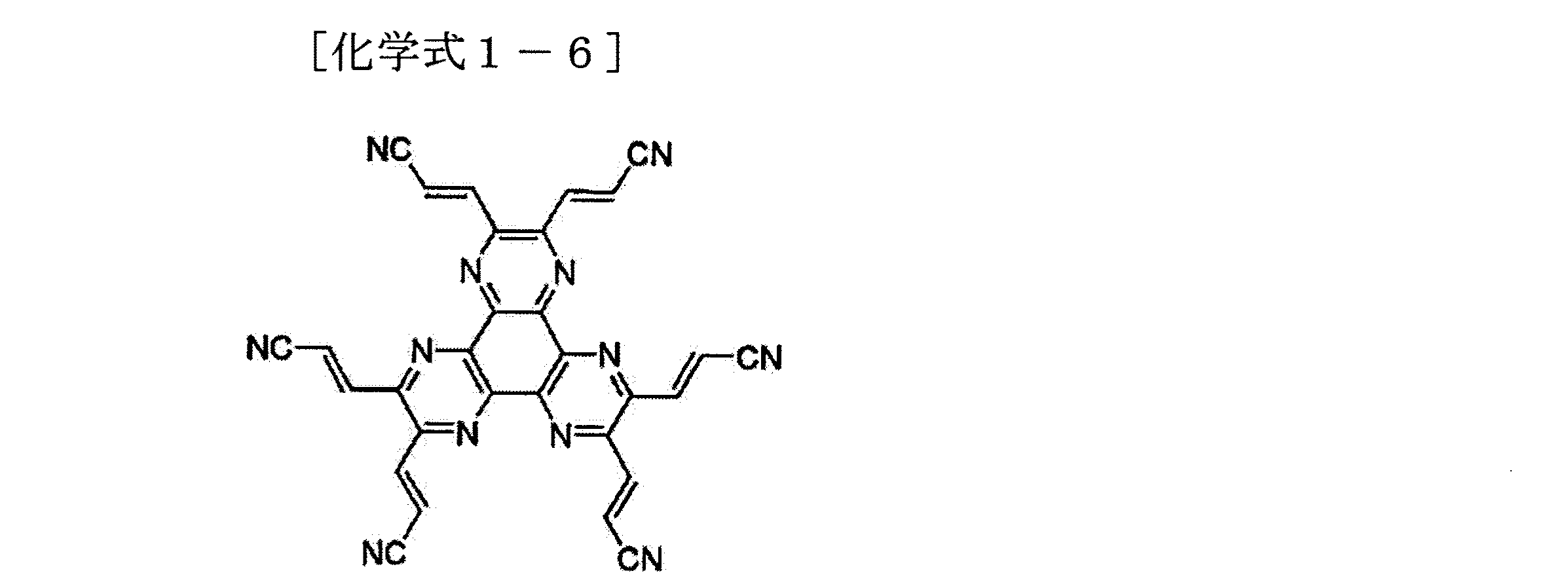
前記化学式1の化合物の具体的な例としては、下記化学式の化合物がある。
前記化学式1の他の例や合成方法および多様な特徴は、米国特許出願第2002−0158242号、米国特許第6,436,559号および米国特許第4,780,536号に記載されており、これら文献の内容は全て本明細書に含まれる。 Other examples, synthesis methods, and various features of Formula 1 are described in U.S. Patent Application No. 2002-0158242, U.S. Patent No. 6,436,559 and U.S. Patent No. 4,780,536. The contents of these documents are all included in this specification.
本発明では前記化学式1の化合物を含むバッファ層の厚さを増加させることによって、前述したバッファ層としての効果を増加させられる。これは前記バッファ層の厚さの増加による漏れ電流の改善効果によってわかる。図6は、基板、陰極、有機物層および陽極が順次積層された構造の有機発光素子において、陽極に接する前記化学式1の化合物を含むバッファ層の厚さによる漏れ電流を示した図である。前記化学式1の化合物層の厚さが5nm〜10nmから50nmに増加するにつれて漏れ電流が急激に減少して、電圧−電流特性が顕著に改善されたことが分かる。本発明において、前記化学式1の化合物を含むバッファ層の最適の厚さは、第2電極形成時に用いるスパッタリング工程の因子、例えば蒸着の速度、RF電力(power)、DC電圧などによって変われる。例えば、一般的に速く蒸着するために高い電圧および電力を用いるスパッタリング工程であるほど最適のバッファ層の厚さは増加する。本発明では前記化学式1の化合物を含むバッファ層の厚さが20nm以上であることが好ましく、50nm以上であることがより好ましい。前記バッファ層の厚さが20nm未満の場合には前記層が正孔注入または輸送層の役割をすることはできるが、バッファ層としての役割は十分にすることができない。一方、前記バッファ層の厚さは250nm以下であることが好ましい。前記層の厚さが250nmを越える場合には素子の製造工程時間が非常に長くなるようになり、化学式1の化合物層の表面形状が粗くなって、素子の他の特性に影響を及ぼせる。 In the present invention, by increasing the thickness of the buffer layer containing the compound of Formula 1, the effect as the buffer layer described above can be increased. This can be seen from the effect of improving the leakage current by increasing the thickness of the buffer layer. FIG. 6 is a diagram illustrating a leakage current according to the thickness of the buffer layer containing the compound of Formula 1 in contact with the anode in the organic light emitting device having a structure in which a substrate, a cathode, an organic material layer, and an anode are sequentially stacked. It can be seen that as the thickness of the compound layer of Formula 1 increases from 5 nm to 10 nm to 50 nm, the leakage current rapidly decreases and the voltage-current characteristics are remarkably improved. In the present invention, the optimum thickness of the buffer layer containing the compound of Formula 1 varies depending on factors of the sputtering process used when forming the second electrode, such as the deposition rate, RF power, and DC voltage. For example, the optimum buffer layer thickness increases with sputtering processes that typically use higher voltages and powers for faster deposition. In the present invention, the thickness of the buffer layer containing the compound of Chemical Formula 1 is preferably 20 nm or more, and more preferably 50 nm or more. When the thickness of the buffer layer is less than 20 nm, the layer can serve as a hole injection or transport layer, but cannot serve as a buffer layer. Meanwhile, the thickness of the buffer layer is preferably 250 nm or less. When the thickness of the layer exceeds 250 nm, the manufacturing process time of the device becomes very long, and the surface shape of the compound layer of Chemical Formula 1 becomes rough, affecting other characteristics of the device.
本発明において、前記化学式1の化合物を含むバッファ層は真空蒸着法や溶液塗布法によって、陽極と陰極との間に形成することによって製造することができる。前記溶液塗布法の例としては、スピンコーティング、ディップコーティング、ドクターブレード、インクジェット印刷または熱転写法などがあり、これらにだけ限定されない。前記化学式1の化合物を含むバッファ層は必要によって他の物質をさらに含むこともでき、前記バッファ層は前記化学式1の有機物と共に無機物を含む有無機混合物質薄膜で形成される。 In the present invention, the buffer layer containing the compound of Chemical Formula 1 can be manufactured by forming between the anode and the cathode by a vacuum deposition method or a solution coating method. Examples of the solution coating method include spin coating, dip coating, doctor blade, ink jet printing, and thermal transfer method, but are not limited thereto. The buffer layer including the compound of Formula 1 may further include other materials as necessary, and the buffer layer is formed of an organic / organic mixed material thin film including an inorganic material together with the organic material of Formula 1.
本発明において、前記第2電極とバッファ層との間に絶縁性質を有する酸化物薄膜がさらに備われる。 In the present invention, an oxide thin film having an insulating property is further provided between the second electrode and the buffer layer.
一方、本発明の有機発光素子において、有機物層は電子輸送層を含むことができ、この電子輸送層はLi、Cs、Na、Mg、Sc、Ca、K、Ce、Euなどのように仕事関数が小さい金属またはこれら金属のうち1種以上の金属薄膜と有機物質を同時蒸着(co−deposition)する方法で形成することができる。ただし、本発明の有機発光素子の電子輸送層は、イミダゾール基、オキサゾール基およびチアゾール基からなる群から選択される基、より好ましくはイミダゾール基を有する物質を含む方が良い。前記物質の例としては、イミダゾール基を有した韓国特許公開第2003−0067773号に記載された下記化学式2の化合物または米国特許第5,645,948号に記載された下記化学式3の化合物などがあり、これはLi、Cs、Na、Mg、Sc、Ca、K、Ce、Euなどのように仕事関数が小さい金属と共に蒸着し得る。前記韓国特許公開第2003−0067773号および米国特許第5,645,948号は全体が本発明の内容に含まれる。
R7およびR8は各々独立したに水素、炭素数1〜20の脂肪族炭化水素、ベンゼン、ナフタレン、ビフェニル、アントラセンのような芳香族環および芳香族複素環からなる群から選択されるものであるが、ただしR7およびR8がともに水素ではなく、
Arはベンゼン、ナフタレン、ビフェニル、アントラセンのような芳香族環および芳香族複素環からなる群から選択され、
R9は水素、炭素数1〜6の脂肪族炭化水素、置換されたベンゼン、ナフタレン、ビフェニル、アントラセンのような芳香族環または芳香族複素環からなる群から選択され、
XはO、SおよびNR10(ここで、R10は水素、炭素数1〜7の脂肪族炭化水素、ベンゼン、ナフタレン、ビフェニル、アントラセンのような芳香族環および芳香族複素環から選択される)からなる群から選択される。
nは3〜8の整数であり、
ZはO、SまたはN−Rであり、
RとR’は各々水素、炭素数1〜24のアルキル、例えばプロピル、t−ブチル、ヘプチルなど、炭素数5〜20のアリールまたはヘテロ原子を含む置換されたアリール、例えばフェニル、ナフチル、フリル、チエニル、ピリジル、キノリニルなど、およびその他複素環系、またはクロロ、フルオロなどのハロゲン、または縮合芳香族環を完成させるのに必要な原子であり、
Bは連結ユニットであって、複数のベンザゾ−ル(benzazole)を共役または非共役連結するアルキル、アリール、置換されたアルキル、または置換されたアリールである。
Meanwhile, in the organic light emitting device of the present invention, the organic material layer may include an electron transport layer, and the electron transport layer has a work function such as Li, Cs, Na, Mg, Sc, Ca, K, Ce, Eu, and the like. Or a metal thin film of one or more of these metals and an organic material can be formed by a co-deposition method. However, the electron transport layer of the organic light-emitting device of the present invention should contain a group selected from the group consisting of an imidazole group, an oxazole group and a thiazole group, more preferably a substance having an imidazole group. Examples of the substance include a compound of the following
R 7 and R 8 are each independently selected from the group consisting of hydrogen, aliphatic hydrocarbons having 1 to 20 carbon atoms, aromatic rings such as benzene, naphthalene, biphenyl, anthracene and aromatic heterocycles. But R 7 and R 8 are not both hydrogen,
Ar is selected from the group consisting of aromatic rings and aromatic heterocycles such as benzene, naphthalene, biphenyl, anthracene,
R 9 is selected from the group consisting of hydrogen, C 1-6 aliphatic hydrocarbons, substituted benzenes, naphthalenes, biphenyls, aromatic rings such as anthracene, or aromatic heterocycles;
X is O, S and NR 10 (where R 10 is selected from hydrogen, aliphatic hydrocarbons having 1 to 7 carbon atoms, aromatic rings such as benzene, naphthalene, biphenyl, anthracene and aromatic heterocycles) ).
n is an integer of 3 to 8,
Z is O, S or N—R;
R and R ′ are each hydrogen, alkyl having 1 to 24 carbon atoms, such as propyl, t-butyl, heptyl, etc., aryl having 5 to 20 carbon atoms or substituted aryl containing a hetero atom such as phenyl, naphthyl, furyl, Thienyl, pyridyl, quinolinyl, and the like, and other heterocyclic ring systems, or halogens such as chloro, fluoro, or atoms necessary to complete a fused aromatic ring,
B is a linking unit, which is an alkyl, aryl, substituted alkyl, or substituted aryl that conjugated or non-conjugatedly connects a plurality of benzazoles.
本発明において、素子の電子輸送層を上記のような物質を含むように構成する場合、この素子は電子注入層を含むことが好ましく、この電子注入層はLiF層であることが好ましい。 In the present invention, when the electron transport layer of the device is configured to include the above-described substances, the device preferably includes an electron injection layer, and the electron injection layer is preferably a LiF layer.
本発明の有機発光素子は基板、第1電極、2層以上の有機物層および第2電極が積層された構造において、前記有機物層のうち第2電極に接する有機物層を前記化学式1の化合物を含むバッファ層として形成することを除いては、当技術分野に知られている材料および方法を用いて製造される。 The organic light emitting device of the present invention includes a substrate, a first electrode, two or more organic layers, and a second electrode, wherein the organic layer in contact with the second electrode of the organic layer includes the compound of Formula 1. It is manufactured using materials and methods known in the art, except that it is formed as a buffer layer.
ただし、上述したように本発明ではバッファ層上に積層する第2電極の形成方法に大きく制限されないため、従来技術と比較して、第2電極の材料および形成工程に対する選択の幅がより広い。 However, as described above, the present invention is not largely limited by the method of forming the second electrode laminated on the buffer layer, and therefore, the selection range for the material and the forming process of the second electrode is wider than that of the prior art.
例えば、本発明で第2電極は、スパッタリング、レーザを用いた物理的蒸着方法(physical vapor deposition; PVD)、イオンビームを用いた蒸着方法(ion beam assisted deposition)またはこれらと類似する方法のように電荷や高い運動エネルギを有する粒子を伴うことによって、有機物層に損傷を与えられる薄膜形成技術を使用でき、したがって、前記方法によってのみ形成可能な電極材料も使用できる。例えば、第2電極はIZOまたはITOなどのように可視光線領域で透明な伝導性酸化物質や、Al、Ag、Au、Ni、Pd、Ti、Mo、Mg、Ca、Zn、Te、Pt、Irまたはこれらのうち1つ以上を含む合金物質で形成することができる。 For example, in the present invention, the second electrode may be formed by sputtering, a physical vapor deposition method (PVD) using a laser, a deposition method using an ion beam (ion beam assisted deposition), or a similar method. By involving particles having a charge and high kinetic energy, it is possible to use a thin film forming technique that can damage the organic layer, and thus electrode materials that can be formed only by the above method can also be used. For example, the second electrode may be a conductive oxide transparent in the visible light region such as IZO or ITO, Al, Ag, Au, Ni, Pd, Ti, Mo, Mg, Ca, Zn, Te, Pt, Ir. Alternatively, it can be formed of an alloy material including one or more of these.
本発明に係わる有機発光素子の例を図4および図5に示した。図4は、前面発光素子を例示した図であり、図5は、両面発光素子を例示した図である。しかし、本発明の有機発光素子の構造がこれらだけに限定されることはない。 Examples of the organic light emitting device according to the present invention are shown in FIGS. FIG. 4 is a diagram illustrating a front light emitting device, and FIG. 5 is a diagram illustrating a double-sided light emitting device. However, the structure of the organic light emitting device of the present invention is not limited to these.
本発明の有機発光素子中の有機物層は、1層構造からなることもできるが、2層以上の有機物層が積層された多層構造からなることもできる。例えば、本発明の有機発光素子は、有機物層として正孔注入層、正孔輸送層、発光層、電子輸送層、電子注入層および陽極と正孔注入層との間の緩衝層などを含む構造を有することができる。しかし、有機発光素子の構造は、これに限定されることはなく、さらに少ない数の有機物層を含むことができる。 The organic material layer in the organic light emitting device of the present invention can have a single layer structure, but can also have a multilayer structure in which two or more organic material layers are laminated. For example, the organic light emitting device of the present invention has a structure including a hole injection layer, a hole transport layer, a light emitting layer, an electron transport layer, an electron injection layer, and a buffer layer between the anode and the hole injection layer as the organic material layer. Can have. However, the structure of the organic light emitting device is not limited to this, and may include a smaller number of organic layers.
以下では、実施例を介して本発明をより詳しく説明する。しかし、下記実施例は本発明を例示するだけで、本発明の範囲が下記実施例によって限定されることはない。 In the following, the present invention will be described in more detail through examples. However, the following examples only illustrate the present invention, and the scope of the present invention is not limited by the following examples.
実施例1〜5
ガラス基板上に熱的蒸着(thermal evaporation)工程を用いて、150nm厚さの陰極(Al)と1.5nm厚さの電子注入層(LiF)を順に形成した。続いて、前記電子注入層上に電子輸送層としては下記化学式2−1で表示されるイミダゾール基を含む物質の薄膜を20nm厚さで形成して用いた。
A 150 nm-thick cathode (Al) and a 1.5 nm-thick electron injection layer (LiF) were sequentially formed on a glass substrate by using a thermal evaporation process. Subsequently, a thin film of a substance containing an imidazole group represented by the following chemical formula 2-1 was formed to a thickness of 20 nm on the electron injection layer as the electron transport layer.
次に、前記電子輸送層上にAlq3発光ホストにC545T(10−(2−benzothiazolyl)−1,1,7,7−tetramethyl−2,3,6,7−tetrahyro−1H,5H,11H−1)benzo pyrano[6,7,8−ij]quinolizin−11−one)を1重量%で同時蒸着(co−deposition)して、30nm厚さの発光層を形成した。発光層上に正孔輸送層として40nm厚さのNPB(4,4’−ビス[N−(1−ナフチル)−N−フェニルアミノ]ビフェニル)薄膜を蒸着した。正孔輸送層上に正孔注入層およびバッファ層として下記化学式1−1の化合物を用いて5nm(実施例1)、10nm(実施例2)、20nm(実施例3)、50nm(実施例4)および70nm(実施例5)厚さの層を形成した。
前記バッファ層上にスパッタリング法を用いて、秒当たり1.3Åの速度で150nm厚さのIZO陽極を形成して、前面発光有機発光素子を製造した。 A front-emitting organic light-emitting device was manufactured by forming a 150 nm thick IZO anode on the buffer layer using a sputtering method at a rate of 1.3 mm per second.
実施例6
陰極として150nm厚さのAl薄膜の代わりに150nm厚さのITO上に5nm厚さの非常に薄いAl薄膜を形成した陰極を用いたことを除いては、実施例1〜5と同一の方法で実施して、両面発光有機発光素子を製造した。
Example 6
The same method as in Examples 1 to 5 except that a cathode in which a very thin Al thin film having a thickness of 5 nm was formed on ITO having a thickness of 150 nm was used as the cathode instead of the Al thin film having a thickness of 150 nm. As a result, a double-sided light emitting organic light emitting device was manufactured.
[素子の電流−電圧特性および発光特性測定]
実施例1で製造された有機発光素子に逆方向および正方向の電界を0.2Volt間隔で順次印加しながら各電圧値での電流を測定し、その結果を各々図6および図7に示した。また、実施例1で製造された有機発光素子に電流密度を10mA/cm2から100mA/cm2まで順次印加しながら発光量を光度法(photometry)で測定し、その結果を図8および図9に示した。
[Measurement of current-voltage characteristics and light emission characteristics of elements]
The current at each voltage value was measured while sequentially applying reverse and forward electric fields at 0.2 Volt intervals to the organic light emitting device manufactured in Example 1, and the results are shown in FIGS. 6 and 7, respectively. . Further, the light emission amount while sequentially applying a current density in the organic light-emitting device prepared in Example 1 from 10 mA / cm 2 until 100 mA / cm 2 measured by the photometric method (Photometry), FIGS. 8 and the result 9 It was shown to.
有機発光素子において、電極形成時に有機物層が損傷すれば電流−電圧特性および発光特性が低下するため、図6〜9に示した電流−電圧特性および発光特性は化学式1の化合物による有機物層の損傷防止効果を示すのである。 In the organic light emitting device, if the organic layer is damaged when the electrode is formed, the current-voltage characteristics and the light emitting characteristics are deteriorated. Therefore, the current-voltage characteristics and the light emitting characteristics shown in FIGS. It shows the prevention effect.
図6および図7は、本発明に係わるバッファ層の厚さによる有機発光素子の電流−電圧特性を示した図である。基板と反対側に位置する第2電極に接する有機物層が、通常従来の有機発光素子で用いられてきた有機物からなる場合には、前記有機物層上にスパッタリング法で第2電極を形成すれば、有機物層の損傷によって発光素子が正常な整流特性および発光特性を表わさないと知られている。しかし、図6および図7に示したように、前記化学式1の化合物からなるバッファ層の厚さが増加するにつれて有機発光素子の固有の素子特性、すなわち整流特性を明確に示した。 6 and 7 are diagrams illustrating current-voltage characteristics of the organic light emitting device according to the thickness of the buffer layer according to the present invention. When the organic layer in contact with the second electrode located on the opposite side of the substrate is made of an organic material that is usually used in a conventional organic light emitting device, the second electrode is formed on the organic layer by a sputtering method. It is known that a light-emitting element does not exhibit normal rectification characteristics and light-emitting characteristics due to damage of an organic layer. However, as shown in FIGS. 6 and 7, the intrinsic device characteristic of the organic light emitting device, that is, the rectifying property is clearly shown as the thickness of the buffer layer made of the compound of Formula 1 increases.
まず、図6の逆方向電流−電圧特性を見てみると、化学式1の化合物を含むバッファ層の厚さを5nm〜10nm程度の厚さで形成した場合素子の漏れ電流が少しずつ改善され、50nm以上の厚さで形成した場合素子の漏れ電流が顕著に改善され、非常に明確な整流特性を示した。図7の正方向電流−電圧特性を見れば、前記化学式1の化合物層の厚さが10nmから50nmに増加しながら電流が急激に増加している。 First, looking at the reverse current-voltage characteristics of FIG. 6, when the thickness of the buffer layer containing the compound of Chemical Formula 1 is formed with a thickness of about 5 nm to 10 nm, the leakage current of the device is gradually improved. When formed with a thickness of 50 nm or more, the leakage current of the device was remarkably improved, and very clear rectification characteristics were exhibited. Referring to the positive current-voltage characteristics of FIG. 7, the current increases rapidly while the thickness of the compound layer of Chemical Formula 1 increases from 10 nm to 50 nm.
また、上記のような電流増加に比例して、図8に示すように発光特性も改善された。図9の発光効率を見れば、前記化学式1の化合物を含むバッファ層の厚さ増加により発光効率が顕著に増加しており、これは前記バッファ層のスパッタリング損傷防止効果によるものである。 In addition, the light emission characteristics were improved in proportion to the increase in current as shown in FIG. Referring to the luminous efficiency of FIG. 9, the luminous efficiency is remarkably increased by increasing the thickness of the buffer layer containing the compound of Chemical Formula 1, which is due to the effect of preventing sputtering damage of the buffer layer.
実施例7
ガラス基板上に熱的蒸着工程を用いて、150nm厚さの陰極(Al)と1.5nm厚さの電子注入層(LiF)を順に形成した。続いて、前記電子注入層上に電子輸送層として前記化学式2−1で表示されるイミダゾール基を含む物質の薄膜を150nm厚さで形成した。電子輸送層上に1.5nm電子注入層(LiF)層と150nmのAl層を順に形成し、電子によってのみ電流が流れることができる図13のような対称形素子を製造した。
Example 7
A 150 nm-thick cathode (Al) and a 1.5 nm-thick electron injection layer (LiF) were sequentially formed on a glass substrate using a thermal evaporation process. Subsequently, a thin film of a substance containing an imidazole group represented by the chemical formula 2-1 was formed as an electron transport layer on the electron injection layer with a thickness of 150 nm. A 1.5 nm electron injection layer (LiF) layer and a 150 nm Al layer were formed in this order on the electron transport layer, and a symmetrical element as shown in FIG. 13 in which current can flow only by electrons was manufactured.
比較例1
電子輸送層の形成時に化学式2−1の化合物の代わりにAlq3を用いたことを除いては、実施例7と同一の方法を用いて、電子によってのみ電流が流れることができる図13のような対称形素子を製造した。
Comparative Example 1
A current can flow only by electrons using the same method as in Example 7 except that Alq3 was used instead of the compound of Formula 2-1 when forming the electron transport layer as shown in FIG. A symmetrical element was produced.
[素子の電流−電圧特性]
実施例7および比較例1の素子の場合、Al−LiF−電子輸送物質−LiF−Al構造で対称的な素子を製作し、この時電子輸送物質を通して流れる電流は電子によってのみ発生する。
[Element current-voltage characteristics]
In the case of the device of Example 7 and Comparative Example 1, a symmetric device having an Al-LiF-electron transport material-LiF-Al structure is fabricated, and current flowing through the electron transport material is generated only by electrons.
図14は実施例7および比較例1の電流電圧特性を比較して示した図である。図14において、陽の電圧は上部のAl電極から電子輸送層への電子注入の場合であり、陰の電圧は下部のAl電極から電子輸送層への電子注入の場合を示す。電子輸送層物質として有機発光素子で多く用いられているAlq3を用いた比較例1の場合、対称形素子であるにもかかわらず、上部Al電極からの電子注入はよくできる反面、下部Al電極からの電子注入はよくできないことが分かる。一方、電子輸送層物質として化学式2−1の物質を用いた実施例7の場合、電流電圧特性が対称的に表れており、これは上部Al電極および下部Al電極の各々から電子輸送層への電子注入が全てよくできることを示す。 FIG. 14 is a diagram comparing the current-voltage characteristics of Example 7 and Comparative Example 1. In FIG. 14, the positive voltage indicates the case of electron injection from the upper Al electrode to the electron transport layer, and the negative voltage indicates the case of electron injection from the lower Al electrode to the electron transport layer. In the case of Comparative Example 1 using Alq3 which is often used in an organic light emitting device as an electron transport layer material, although it is a symmetrical device, electron injection from the upper Al electrode can be performed well, but from the lower Al electrode. It can be seen that electron injection cannot be performed well. On the other hand, in the case of Example 7 using the substance of the chemical formula 2-1 as the electron transport layer material, the current-voltage characteristics appear symmetrically, and this is from the upper Al electrode and the lower Al electrode to the electron transport layer. It shows that electron injection is all good.
Alq3より化学式2−1の化合物によって下部電極から電子輸送層への電子注入がよくできることは、化学式2−1の化合物の構造中、イミダゾール基がフッ化リチウム(LiF)のLiイオンとの反応性がAlq3よりさらに大きいためであると見なされる。したがって、イミダゾール基などLiイオンとの反応性が大きい基を有する電子輸送物質として用いる場合、下部電極から電子輸送層への電子注入特性を改善できるということが分かる。 The fact that the injection of electrons from the lower electrode to the electron transport layer can be better performed by the compound of Chemical Formula 2-1 than Alq3 is that the imidazole group is reactive with Li ions of lithium fluoride (LiF) in the structure of the compound of Chemical Formula 2-1. Is considered to be larger than Alq3. Therefore, it can be seen that, when used as an electron transport material having a group having high reactivity with Li ions such as an imidazole group, the electron injection characteristics from the lower electrode to the electron transport layer can be improved.
逆構造の有機発光素子の場合、下部電極から電子輸送層への電子注入を必要とするため、上記で述べたように、化学式2または化学式3のようなイミダゾール基、またはこれと類似する特性を有するオキサゾール基、チアゾール基群を含んでいる電子輸送物質を用いるようになれば電子注入特性が良い有機発光素子を得ることができる。
In the case of an organic light emitting device having a reverse structure, since electron injection from the lower electrode to the electron transport layer is required, as described above, an imidazole group such as
本発明では前記化学式1の化合物を含むバッファ層によって、有機物層上の電極形成時に発生できる有機物層の損傷を防止することができる。これによって、有機物層上に電極形成時に発生できる有機物層の損傷なしで基板、陰極、有機物層および陽極が順次積層された構造の有機発光素子を製造することができる。また、このような逆構造の有機発光素子において、化学式2または化学式3のようにイミダゾール基、オキサゾール基またはチアゾール基を含んでいる電子輸送物質を用いるようになれば下部陰極電極から電子輸送層への電子注入特性を向上させ、低電圧で作動する逆構造の有機発光素子を製造することができる。
In the present invention, the buffer layer containing the compound of Chemical Formula 1 can prevent damage to the organic material layer that may occur during electrode formation on the organic material layer. Accordingly, it is possible to manufacture an organic light emitting device having a structure in which a substrate, a cathode, an organic material layer, and an anode are sequentially laminated on the organic material layer without damage to the organic material layer that can occur when forming the electrode. In addition, in such an organic light emitting device having an inverted structure, if an electron transport material containing an imidazole group, an oxazole group or a thiazole group is used as represented by
Claims (18)
前記有機物層が発光層を含み、前記有機物層のうち第2電極に接する有機物層が下記化学式1の化合物を含むバッファ層であることを特徴とする、有機発光素子。
R1〜R6は各々水素、ハロゲン原子、ニトリル(−CN)、ニトロ(−NO2)、スルホニル(−SO2R)、スルホキシド(−SOR)、スルホンアミド(−SO2NR)、スルホネート(−SO3R)、トリフルオロメチル(−CF3)、エステル(−COOR)、アミド(−CONHRまたは−CONRR’)、置換または非置換された直鎖または分枝鎖のC1−C12アルコキシ、置換または非置換された直鎖または分枝鎖C1−C12のアルキル、置換または非置換された芳香族または非芳香族の複素環、置換または非置換されたアリール、置換または非置換されたモノ−またはジ−アリールアミン、および置換または非置換されたアラルキルアミンで構成された群から選択されてなり、
前記RおよびR’は各々置換または非置換されたC1−C60のアルキル、置換または非置換されたアリールおよび置換または非置換の5−7元の複素環からなる群から選択されてなるものである。] An organic light emitting device comprising a substrate, a first electrode, an organic material layer composed of two or more layers, and a second electrode, which are sequentially laminated,
The organic light emitting device, wherein the organic material layer includes a light emitting layer, and the organic material layer in contact with the second electrode of the organic material layer is a buffer layer containing a compound of the following chemical formula 1.
R 1 to R 6 are each hydrogen, a halogen atom, nitrile (—CN), nitro (—NO 2 ), sulfonyl (—SO 2 R), sulfoxide (—SOR), sulfonamide (—SO 2 NR), sulfonate ( -SO 3 R), trifluoromethyl (-CF 3), ester (-COOR), amide (-CONHR or -CONRR '), substituted or unsubstituted straight or C 1 -C 12 alkoxy branched Substituted or unsubstituted linear or branched C 1 -C 12 alkyl, substituted or unsubstituted aromatic or non-aromatic heterocycle, substituted or unsubstituted aryl, substituted or unsubstituted Selected from the group consisting of a mono- or di-arylamine, and a substituted or unsubstituted aralkylamine;
R and R ′ are each selected from the group consisting of substituted or unsubstituted C 1 -C 60 alkyl, substituted or unsubstituted aryl, and substituted or unsubstituted 5-7 original heterocycle It is. ]
R7およびR8は各々独立したに水素、炭素数1〜20の脂肪族炭化水素、芳香族環および芳香族複素環からなる群から選択されるものであるが、ただしR7およびR8がともに水素ではなく、
Arは芳香族環および芳香族複素環からなる群から選択され、
R9は水素、炭素数1〜6の脂肪族炭化水素、芳香族環または芳香族複素環からなる群から選択され、
XはO、SおよびNR10(ここで、R10は水素、炭素数1〜7の脂肪族炭化水素、芳香族環および芳香族複素環から選択される)からなる群から選択されてなるものである。]
nは3〜8の整数であり、
ZはO、SまたはN−Rであり、
RとR’は各々水素、炭素数1〜24のアルキル、炭素数5〜20のアリールまたはヘテロ原子を含む置換されたアリール、またはハロゲン、または縮合芳香族環を完成させるのに必要な原子であり、
Bは連結ユニットとして、複数のベンザゾ−ルを共役または非共役連結するアルキル、アリール、置換されたアルキル、または置換されたアリールである。] The organic light emitting device according to claim 13, wherein the electron transport layer includes a compound selected from the group consisting of a compound of the following chemical formula 2 and a compound of the chemical formula 3.
R 7 and R 8 are each independently selected from the group consisting of hydrogen, aliphatic hydrocarbons having 1 to 20 carbon atoms, aromatic rings and aromatic heterocycles, provided that R 7 and R 8 are Both are not hydrogen,
Ar is selected from the group consisting of aromatic rings and aromatic heterocycles;
R 9 is selected from the group consisting of hydrogen, an aliphatic hydrocarbon having 1 to 6 carbon atoms, an aromatic ring or an aromatic heterocyclic ring;
X is selected from the group consisting of O, S and NR 10 (wherein R 10 is selected from hydrogen, an aliphatic hydrocarbon having 1 to 7 carbon atoms, an aromatic ring and an aromatic heterocyclic ring) It is. ]
n is an integer of 3 to 8,
Z is O, S or N—R;
R and R ′ are each hydrogen, substituted alkyl containing 1 to 24 carbon atoms, substituted aryl containing 5 to 20 carbon atoms or heteroatoms, or halogen, or atoms necessary to complete a fused aromatic ring. Yes,
B is an alkyl, aryl, substituted alkyl, or substituted aryl that links or conjugates a plurality of benzazoles as a linking unit. ]
前記有機物層のうち1層を発光層で形成し、前記有機物層のうち第2電極に接する有機物層を下記化学式1の化合物を用いて形成することを特徴とする、製造方法。
R1〜R6は各々水素、ハロゲン原子、ニトリル(−CN)、ニトロ(−NO2)、スルホニル(−SO2R)、スルホキシド(−SOR)、スルホンアミド(−SO2NR)、スルホネート(−SO3R)、トリフルオロメチル(−CF3)、エステル(−COOR)、アミド(−CONHRまたは−CONRR’)、置換または非置換された直鎖または分枝鎖のC1−C12アルコキシ、置換または非置換された直鎖または分枝鎖C1−C12のアルキル、置換または非置換された芳香族または非芳香族の複素環、置換または非置換されたアリール、置換または非置換されたモノ−またはジ−アリールアミン、および置換または非置換されたアラルキルアミンで構成された群から選択されてなり、
前記RおよびR’は各々置換または非置換されたC1−C60のアルキル、置換または非置換されたアリールおよび置換または非置換の5−7元の複素環からなる群から選択されてなるものである。] A method of manufacturing an organic light emitting device comprising a step of sequentially stacking and forming a first electrode, an organic material layer composed of two or more layers, and a second electrode on a substrate,
One of the organic layers is formed by a light emitting layer, and the organic layer in contact with the second electrode is formed by using a compound of the following chemical formula 1 among the organic layers.
R 1 to R 6 are each hydrogen, halogen atom, nitrile (—CN), nitro (—NO 2 ), sulfonyl (—SO 2 R), sulfoxide (—SOR), sulfonamide (—SO 2 NR), sulfonate ( -SO 3 R), trifluoromethyl (-CF 3), ester (-COOR), amide (-CONHR or -CONRR '), substituted or unsubstituted straight or C 1 -C 12 alkoxy branched Substituted or unsubstituted linear or branched C 1 -C 12 alkyl, substituted or unsubstituted aromatic or non-aromatic heterocycle, substituted or unsubstituted aryl, substituted or unsubstituted Selected from the group consisting of: mono- or di-arylamines, and substituted or unsubstituted aralkylamines;
R and R ′ are each selected from the group consisting of substituted or unsubstituted C 1 -C 60 alkyl, substituted or unsubstituted aryl, and substituted or unsubstituted 5-7 original heterocycle It is. ]
Applications Claiming Priority (2)
| Application Number | Priority Date | Filing Date | Title |
|---|---|---|---|
| KR20040065517 | 2004-08-19 | ||
| PCT/KR2005/002718 WO2006019270A1 (en) | 2004-08-19 | 2005-08-18 | Organic light-emitting device comprising buffer layer and method for fabricating the same |
Related Child Applications (1)
| Application Number | Title | Priority Date | Filing Date |
|---|---|---|---|
| JP2012172291A Division JP5912977B2 (en) | 2004-08-19 | 2012-08-02 | Organic light emitting device including buffer layer and method of manufacturing the same |
Publications (1)
| Publication Number | Publication Date |
|---|---|
| JP2008510312A true JP2008510312A (en) | 2008-04-03 |
Family
ID=35907633
Family Applications (2)
| Application Number | Title | Priority Date | Filing Date |
|---|---|---|---|
| JP2007527054A Pending JP2008510312A (en) | 2004-08-19 | 2005-08-18 | Organic light emitting device including buffer layer and method of manufacturing the same |
| JP2012172291A Active JP5912977B2 (en) | 2004-08-19 | 2012-08-02 | Organic light emitting device including buffer layer and method of manufacturing the same |
Family Applications After (1)
| Application Number | Title | Priority Date | Filing Date |
|---|---|---|---|
| JP2012172291A Active JP5912977B2 (en) | 2004-08-19 | 2012-08-02 | Organic light emitting device including buffer layer and method of manufacturing the same |
Country Status (7)
| Country | Link |
|---|---|
| US (1) | US7763882B2 (en) |
| EP (1) | EP1794255B1 (en) |
| JP (2) | JP2008510312A (en) |
| KR (1) | KR100718765B1 (en) |
| CN (1) | CN101006159B (en) |
| TW (1) | TWI345583B (en) |
| WO (1) | WO2006019270A1 (en) |
Cited By (4)
| Publication number | Priority date | Publication date | Assignee | Title |
|---|---|---|---|---|
| JP2009515358A (en) * | 2005-11-07 | 2009-04-09 | エルジー・ケム・リミテッド | ORGANIC LIGHT EMITTING DEVICE AND MANUFACTURING METHOD THEREOF |
| JP2011501432A (en) * | 2007-10-16 | 2011-01-06 | グローバル・オーエルイーディー・テクノロジー・リミテッド・ライアビリティ・カンパニー | Inverted OLED device with improved efficiency |
| JP2012504847A (en) * | 2008-10-01 | 2012-02-23 | エルジー・ケム・リミテッド | ORGANIC LIGHT EMITTING ELEMENT AND MANUFACTURING METHOD THEREOF |
| JP2013033728A (en) * | 2011-07-01 | 2013-02-14 | Semiconductor Energy Lab Co Ltd | Light-emitting device, electronic appliance, and illumination device |
Families Citing this family (44)
| Publication number | Priority date | Publication date | Assignee | Title |
|---|---|---|---|---|
| KR100721656B1 (en) | 2005-11-01 | 2007-05-23 | 주식회사 엘지화학 | Organic electronic devices |
| US7560175B2 (en) * | 1999-12-31 | 2009-07-14 | Lg Chem, Ltd. | Electroluminescent devices with low work function anode |
| KR100377321B1 (en) * | 1999-12-31 | 2003-03-26 | 주식회사 엘지화학 | Electronic device comprising organic compound having p-type semiconducting characteristics |
| JP2008510312A (en) | 2004-08-19 | 2008-04-03 | エルジー・ケム・リミテッド | Organic light emitting device including buffer layer and method of manufacturing the same |
| KR100845694B1 (en) | 2006-01-18 | 2008-07-11 | 주식회사 엘지화학 | Oled having stacked organic light-emitting units |
| CA2641880C (en) | 2006-02-10 | 2014-09-09 | Summit Corporation Plc | Treatment of duchenne muscular dystrophy |
| CN101473464B (en) | 2006-06-22 | 2014-04-23 | 出光兴产株式会社 | Organic electroluminescent element using heterocyclic aromatic amine derivative |
| KR101254589B1 (en) * | 2006-06-29 | 2013-04-15 | 엘지디스플레이 주식회사 | The organic electro-luminescence device and method for fabricating of the same |
| SI2170396T1 (en) * | 2007-08-03 | 2017-04-26 | Summit (Oxford) Limited | Drug combinations for the treatment of duchenne muscular dystrophy |
| GB0715937D0 (en) * | 2007-08-15 | 2007-09-26 | Vastox Plc | Method of treatment og duchenne muscular dystrophy |
| US20090091242A1 (en) * | 2007-10-05 | 2009-04-09 | Liang-Sheng Liao | Hole-injecting layer in oleds |
| US9071809B2 (en) * | 2008-01-04 | 2015-06-30 | Nanolumens Acquisition, Inc. | Mobile, personsize display system and method of use |
| KR101003232B1 (en) * | 2008-01-23 | 2010-12-21 | 주식회사 엘지화학 | Organic electroluminescent device and method for fabricating the same |
| US8178870B2 (en) * | 2008-04-23 | 2012-05-15 | Panasonic Corporation | Organic electroluminescence element |
| KR101128468B1 (en) * | 2009-11-02 | 2012-04-12 | 엘지디스플레이 주식회사 | Organic Light Emitting Display Device |
| KR101391964B1 (en) | 2010-04-02 | 2014-05-07 | 가부시키가이샤 한도오따이 에네루기 켄큐쇼 | semiconductor device |
| US9359505B2 (en) | 2010-07-27 | 2016-06-07 | Konica Minolta Holdings, Inc. | Gas barrier film, process for production of gas barrier film, and electronic device |
| WO2012026362A1 (en) | 2010-08-25 | 2012-03-01 | コニカミノルタホールディングス株式会社 | Method for manufacturing gas barrier film, and organic photoelectric conversion element |
| CN102456839A (en) * | 2010-10-21 | 2012-05-16 | 海洋王照明科技股份有限公司 | Organic electroluminescent device and manufacturing method thereof |
| JP5761203B2 (en) | 2010-12-27 | 2015-08-12 | コニカミノルタ株式会社 | Gas barrier film and electronic device |
| US9362524B2 (en) | 2010-12-27 | 2016-06-07 | Konica Minolta, Inc. | Method for producing gas barrier film, gas barrier film, and electronic device |
| KR20130032675A (en) * | 2011-09-23 | 2013-04-02 | 삼성디스플레이 주식회사 | Dual mode organic light emitting device and pixel circuit including the same |
| US9520576B2 (en) | 2011-11-24 | 2016-12-13 | Konica Minolta, Inc. | Gas barrier film and electronic apparatus |
| KR101407588B1 (en) | 2011-12-27 | 2014-06-13 | 에스에프씨 주식회사 | A condensed-cyclic compound and an organic light emitting diode comprising the same |
| CN102651455B (en) * | 2012-02-28 | 2015-11-25 | 京东方科技集团股份有限公司 | OLED, AMOLED device and manufacture method thereof |
| WO2013161166A1 (en) | 2012-04-27 | 2013-10-31 | パナソニック株式会社 | Organic el element, organic el panel provided therewith, organic el light-emitting device, and organic el display |
| EP2851192A4 (en) | 2012-05-14 | 2015-12-23 | Konica Minolta Inc | Gas barrier film, manufacturing method for gas barrier film, and electronic device |
| KR101433524B1 (en) * | 2012-05-25 | 2014-08-22 | 주식회사 엘지화학 | Organic light emitting device and method for manufacturing the same |
| TWI601323B (en) * | 2012-05-31 | 2017-10-01 | 樂金顯示科技股份有限公司 | Organic light emitting device and method for preparing the same |
| CN103183683B (en) * | 2013-01-25 | 2015-07-01 | 深圳市华星光电技术有限公司 | Sulfuryl compound, organic electroluminescence device adopting sulfuryl compound, and preparation method thereof |
| KR102081281B1 (en) * | 2013-02-08 | 2020-05-28 | 삼성디스플레이 주식회사 | Organic light emitting device |
| CN104051640A (en) * | 2013-03-12 | 2014-09-17 | 海洋王照明科技股份有限公司 | Organic electroluminescent device and manufacturing method thereof |
| KR101820038B1 (en) * | 2013-09-30 | 2018-02-28 | 엘지디스플레이 주식회사 | Transparent electrode and organic electronic device comprising the same |
| US9755177B2 (en) * | 2013-10-09 | 2017-09-05 | Sharp Kabushiki Kaisha | Organic electroluminescent display panel |
| CN103996792B (en) * | 2014-04-30 | 2016-04-27 | 京东方科技集团股份有限公司 | Organic luminescent device and manufacture method and organic light-emitting display device and driving method |
| WO2016079957A1 (en) * | 2014-11-17 | 2016-05-26 | 株式会社Joled | Method for manufacturing organic electroluminescence element, and organic electroluminescence element |
| KR102399953B1 (en) * | 2015-08-25 | 2022-05-18 | 엘지디스플레이 주식회사 | Organic light emitting display device |
| KR102519668B1 (en) | 2016-06-21 | 2023-04-07 | 삼성전자주식회사 | Semiconductor light-emitting device and method for manufacturing the same |
| CN106450015B (en) * | 2016-10-11 | 2018-07-10 | 武汉华星光电技术有限公司 | Transparent OLED display and preparation method thereof |
| JP7208148B2 (en) | 2017-11-08 | 2023-01-18 | ソニーグループ株式会社 | Photoelectric conversion element and imaging device |
| KR102191397B1 (en) * | 2018-10-10 | 2020-12-16 | 재단법인대구경북과학기술원 | Perovskite solar cell comprising surface-treated electron transport layer and method of manufacturing the same |
| CN111244317B (en) * | 2018-11-27 | 2022-06-07 | 海思光电子有限公司 | Light emitting device and terminal equipment |
| CN111925366B (en) * | 2019-05-13 | 2024-04-09 | 广东阿格蕾雅光电材料有限公司 | Imidazo nitrogen heterocyclic compound and application thereof |
| US20220123030A1 (en) * | 2020-10-16 | 2022-04-21 | Shenzhen China Star Optoelectronics Semiconductor Display Technology Co., Ltd. | Driving circuit board and method for fabricating same |
Citations (7)
| Publication number | Priority date | Publication date | Assignee | Title |
|---|---|---|---|---|
| JPH0854836A (en) * | 1994-08-10 | 1996-02-27 | Nec Corp | Drive circuit for active matrix type current controlling light emitting element |
| JPH1092578A (en) * | 1996-08-20 | 1998-04-10 | Eastman Kodak Co | Blue-color organic electroluminescent element |
| JP2001527688A (en) * | 1996-12-23 | 2001-12-25 | ザ トラスティーズ オブ プリンストン ユニバーシテイ | Organic light emitting device containing protective layer |
| JP2003519432A (en) * | 1999-12-31 | 2003-06-17 | エルジー・ケミカル・カンパニー・リミテッド | Electronic device comprising an organic compound having p-type semiconductor properties |
| WO2003060956A2 (en) * | 2002-01-18 | 2003-07-24 | Lg Chem, Ltd. | New material for transporting electrons and organic electroluminescent display using the same |
| WO2004054326A2 (en) * | 2002-12-11 | 2004-06-24 | Lg Chem, Ltd. | Electroluminescent devices with low work function anode |
| JP2004227943A (en) * | 2003-01-23 | 2004-08-12 | Fuji Electric Holdings Co Ltd | Organic electroluminescence element and its manufacturing method |
Family Cites Families (62)
| Publication number | Priority date | Publication date | Assignee | Title |
|---|---|---|---|---|
| US4356429A (en) | 1980-07-17 | 1982-10-26 | Eastman Kodak Company | Organic electroluminescent cell |
| US4359507A (en) | 1981-11-19 | 1982-11-16 | Atlantic Richfield Company | Mixed ethylene and propylene carbonate-containing organic polyisocyanate adhesive binder composition |
| US4780536A (en) * | 1986-09-05 | 1988-10-25 | The Ohio State University Research Foundation | Hexaazatriphenylene hexanitrile and its derivatives and their preparations |
| US4769292A (en) | 1987-03-02 | 1988-09-06 | Eastman Kodak Company | Electroluminescent device with modified thin film luminescent zone |
| DE69027697T2 (en) | 1989-03-31 | 1997-01-23 | Toshiba Kawasaki Kk | Organic electroluminescent device |
| JP3076603B2 (en) | 1990-09-20 | 2000-08-14 | 出光興産株式会社 | Organic electroluminescence device |
| US5150006A (en) | 1991-08-01 | 1992-09-22 | Eastman Kodak Company | Blue emitting internal junction organic electroluminescent device (II) |
| JP3300069B2 (en) | 1992-11-19 | 2002-07-08 | パイオニア株式会社 | Organic electroluminescence device |
| JPH0711249A (en) | 1993-04-28 | 1995-01-13 | Mitsui Petrochem Ind Ltd | Thin film electroluminescent element and its production |
| JP3534445B2 (en) | 1993-09-09 | 2004-06-07 | 隆一 山本 | EL device using polythiophene |
| DE59510315D1 (en) | 1994-04-07 | 2002-09-19 | Covion Organic Semiconductors | Spiro compounds and their use as electroluminescent materials |
| JPH08167477A (en) | 1994-10-13 | 1996-06-25 | Tdk Corp | Organic electroluminescence element |
| JP3412076B2 (en) * | 1995-03-08 | 2003-06-03 | 株式会社リコー | Organic EL device |
| US5792568A (en) * | 1995-04-25 | 1998-08-11 | Sharp Kabushiki Kaisha | Organic electroluminescent element |
| JPH08325564A (en) | 1995-06-05 | 1996-12-10 | Nec Corp | Organic thin film el device |
| DE19543637A1 (en) | 1995-11-23 | 1997-05-28 | Basf Ag | Use of organic compounds present in the plastic-columnar discotic liquid crystalline phase for the transport of electrical charges |
| TW365104B (en) | 1996-03-19 | 1999-07-21 | Motorola Inc | Organic electroluminescent device with new hole transporting material |
| US5766779A (en) | 1996-08-20 | 1998-06-16 | Eastman Kodak Company | Electron transporting materials for organic electroluminescent devices |
| US5998803A (en) * | 1997-05-29 | 1999-12-07 | The Trustees Of Princeton University | Organic light emitting device containing a hole injection enhancement layer |
| US5811833A (en) * | 1996-12-23 | 1998-09-22 | University Of So. Ca | Electron transporting and light emitting layers based on organic free radicals |
| US6046543A (en) | 1996-12-23 | 2000-04-04 | The Trustees Of Princeton University | High reliability, high efficiency, integratable organic light emitting devices and methods of producing same |
| EP1019401B1 (en) | 1997-04-25 | 2008-01-16 | Koninklijke Philips Electronics N.V. | Complex comprising a rare-earth metal ion and a complexing moiety |
| US6497969B2 (en) * | 1997-09-05 | 2002-12-24 | Nessdisplay Co., Ltd. | Electroluminescent device having an organic layer including polyimide |
| DE19740792A1 (en) | 1997-09-17 | 1999-04-01 | Bosch Gmbh Robert | Process for generating a plasma by exposure to microwaves |
| US6501217B2 (en) | 1998-02-02 | 2002-12-31 | International Business Machines Corporation | Anode modification for organic light emitting diodes |
| WO1999039393A1 (en) | 1998-02-02 | 1999-08-05 | International Business Machines Corporation | Anode modification for organic light emitting diodes |
| JP3852518B2 (en) | 1998-05-18 | 2006-11-29 | ソニー株式会社 | Organic electroluminescence device |
| US6352777B1 (en) | 1998-08-19 | 2002-03-05 | The Trustees Of Princeton University | Organic photosensitive optoelectronic devices with transparent electrodes |
| JP2000164361A (en) * | 1998-11-25 | 2000-06-16 | Tdk Corp | Organic el element |
| US6656608B1 (en) * | 1998-12-25 | 2003-12-02 | Konica Corporation | Electroluminescent material, electroluminescent element and color conversion filter |
| US6351067B2 (en) | 1999-01-21 | 2002-02-26 | City University Of Hong Kong | Organic electroluminescent device with improved hole injecting structure |
| JP4198253B2 (en) | 1999-02-02 | 2008-12-17 | 出光興産株式会社 | Organic electroluminescence device and method for producing the same |
| CA2377077A1 (en) | 1999-07-19 | 2001-01-25 | Uniax Corporation | Long-lifetime polymer light-emitting devices with improved luminous efficiency and radiance |
| JP3571977B2 (en) * | 1999-11-12 | 2004-09-29 | キヤノン株式会社 | Organic light emitting device |
| US6953947B2 (en) * | 1999-12-31 | 2005-10-11 | Lg Chem, Ltd. | Organic thin film transistor |
| TWI238183B (en) * | 2000-01-12 | 2005-08-21 | Sumitomo Chemical Co | Polymeric fluorescent substance and polymer light-emitting device |
| AT410729B (en) | 2000-04-27 | 2003-07-25 | Qsel Quantum Solar Energy Linz | PHOTOVOLTAIC CELL WITH A PHOTOACTIVE LAYER OF TWO MOLECULAR ORGANIC COMPONENTS |
| US6579629B1 (en) | 2000-08-11 | 2003-06-17 | Eastman Kodak Company | Cathode layer in organic light-emitting diode devices |
| JP4434460B2 (en) | 2000-09-20 | 2010-03-17 | 京セラ株式会社 | Organic electroluminescence device |
| JP2002208486A (en) | 2001-01-09 | 2002-07-26 | Canon Inc | Organic electronic device |
| JP2002246184A (en) | 2001-02-14 | 2002-08-30 | Fuji Photo Film Co Ltd | Light-emitting element |
| US6998487B2 (en) | 2001-04-27 | 2006-02-14 | Lg Chem, Ltd. | Double-spiro organic compounds and organic electroluminescent devices using the same |
| DE10135513B4 (en) | 2001-07-20 | 2005-02-24 | Novaled Gmbh | Light-emitting component with organic layers |
| JP2003109757A (en) * | 2001-09-28 | 2003-04-11 | Sanyo Electric Co Ltd | Organic electroluminescent element |
| DE10207859A1 (en) | 2002-02-20 | 2003-09-04 | Univ Dresden Tech | Doped organic semiconductor material and process for its production |
| JP2003249353A (en) * | 2002-02-26 | 2003-09-05 | Sharp Corp | Active matrix driven organic led display device and its manufacturing method |
| CN1161002C (en) | 2002-04-03 | 2004-08-04 | 清华大学 | Organic electroluminescent device |
| AU2003230308A1 (en) | 2002-05-07 | 2003-11-11 | Lg Chem, Ltd. | New organic compounds for electroluminescence and organic electroluminescent devices using the same |
| FR2845334B1 (en) * | 2002-10-02 | 2004-11-19 | Plastic Omnium Cie | VEHICLE BUMPER COMPRISING A SPOILER ARTICULATED BETWEEN THREE STABLE BALANCE POSITIONS |
| US6713781B1 (en) | 2002-12-04 | 2004-03-30 | Canon Kabushiki Kaisha | Organic light-emitting device having phenanthroline-fused phenazine |
| US7029765B2 (en) | 2003-04-22 | 2006-04-18 | Universal Display Corporation | Organic light emitting devices having reduced pixel shrinkage |
| JP3902566B2 (en) | 2003-04-24 | 2007-04-11 | 富士電機ホールディングス株式会社 | Organic EL light emitting device |
| US6875320B2 (en) | 2003-05-05 | 2005-04-05 | Eastman Kodak Company | Highly transparent top electrode for OLED device |
| JP3755521B2 (en) | 2003-06-13 | 2006-03-15 | セイコーエプソン株式会社 | ORGANIC EL DEVICE AND ITS DRIVE METHOD, LIGHTING DEVICE, AND ELECTRONIC DEVICE |
| US6963081B2 (en) | 2003-09-30 | 2005-11-08 | Osram Otpo Semiconductors Gmbh | Interfacial trap layer to improve carrier injection |
| DE10357044A1 (en) | 2003-12-04 | 2005-07-14 | Novaled Gmbh | Process for doping organic semiconductors with quinonediimine derivatives |
| JP4276109B2 (en) | 2004-03-01 | 2009-06-10 | ローム株式会社 | Organic electroluminescent device |
| JP2005277282A (en) | 2004-03-26 | 2005-10-06 | Canon Inc | Organic semiconductor device and its manufacturing method |
| KR100690348B1 (en) | 2004-05-11 | 2007-03-09 | 주식회사 엘지화학 | Organic electronic devices |
| KR101249172B1 (en) * | 2004-07-30 | 2013-03-29 | 산요덴키가부시키가이샤 | Organic electroluminescence device |
| JP2008510312A (en) | 2004-08-19 | 2008-04-03 | エルジー・ケム・リミテッド | Organic light emitting device including buffer layer and method of manufacturing the same |
| TWI321968B (en) | 2005-07-15 | 2010-03-11 | Lg Chemical Ltd | Organic light meitting device and method for manufacturing the same |
-
2005
- 2005-08-18 JP JP2007527054A patent/JP2008510312A/en active Pending
- 2005-08-18 WO PCT/KR2005/002718 patent/WO2006019270A1/en active Application Filing
- 2005-08-18 EP EP05780608.5A patent/EP1794255B1/en active Active
- 2005-08-18 CN CN2005800283546A patent/CN101006159B/en active Active
- 2005-08-18 KR KR1020050075849A patent/KR100718765B1/en active IP Right Grant
- 2005-08-19 TW TW094128534A patent/TWI345583B/en active
- 2005-08-19 US US11/206,754 patent/US7763882B2/en not_active Expired - Fee Related
-
2012
- 2012-08-02 JP JP2012172291A patent/JP5912977B2/en active Active
Patent Citations (8)
| Publication number | Priority date | Publication date | Assignee | Title |
|---|---|---|---|---|
| JPH0854836A (en) * | 1994-08-10 | 1996-02-27 | Nec Corp | Drive circuit for active matrix type current controlling light emitting element |
| JPH1092578A (en) * | 1996-08-20 | 1998-04-10 | Eastman Kodak Co | Blue-color organic electroluminescent element |
| JP2001527688A (en) * | 1996-12-23 | 2001-12-25 | ザ トラスティーズ オブ プリンストン ユニバーシテイ | Organic light emitting device containing protective layer |
| JP2003519432A (en) * | 1999-12-31 | 2003-06-17 | エルジー・ケミカル・カンパニー・リミテッド | Electronic device comprising an organic compound having p-type semiconductor properties |
| WO2003060956A2 (en) * | 2002-01-18 | 2003-07-24 | Lg Chem, Ltd. | New material for transporting electrons and organic electroluminescent display using the same |
| JP2005515233A (en) * | 2002-01-18 | 2005-05-26 | エルジー ケミカル エルティーディー. | New electron transport material and organic light emitting device using the same |
| WO2004054326A2 (en) * | 2002-12-11 | 2004-06-24 | Lg Chem, Ltd. | Electroluminescent devices with low work function anode |
| JP2004227943A (en) * | 2003-01-23 | 2004-08-12 | Fuji Electric Holdings Co Ltd | Organic electroluminescence element and its manufacturing method |
Cited By (6)
| Publication number | Priority date | Publication date | Assignee | Title |
|---|---|---|---|---|
| JP2009515358A (en) * | 2005-11-07 | 2009-04-09 | エルジー・ケム・リミテッド | ORGANIC LIGHT EMITTING DEVICE AND MANUFACTURING METHOD THEREOF |
| JP2011501432A (en) * | 2007-10-16 | 2011-01-06 | グローバル・オーエルイーディー・テクノロジー・リミテッド・ライアビリティ・カンパニー | Inverted OLED device with improved efficiency |
| JP2012504847A (en) * | 2008-10-01 | 2012-02-23 | エルジー・ケム・リミテッド | ORGANIC LIGHT EMITTING ELEMENT AND MANUFACTURING METHOD THEREOF |
| JP2015053493A (en) * | 2008-10-01 | 2015-03-19 | エルジー・ケム・リミテッド | Organic light emitting element and method of manufacturing the same |
| US9587172B2 (en) | 2008-10-01 | 2017-03-07 | Lg Display Co., Ltd. | Organic light-emitting diode and method of manufacturing the same |
| JP2013033728A (en) * | 2011-07-01 | 2013-02-14 | Semiconductor Energy Lab Co Ltd | Light-emitting device, electronic appliance, and illumination device |
Also Published As
| Publication number | Publication date |
|---|---|
| WO2006019270A1 (en) | 2006-02-23 |
| TWI345583B (en) | 2011-07-21 |
| EP1794255B1 (en) | 2016-11-16 |
| TW200610807A (en) | 2006-04-01 |
| KR20060053119A (en) | 2006-05-19 |
| US20060038484A1 (en) | 2006-02-23 |
| JP2013016815A (en) | 2013-01-24 |
| KR100718765B1 (en) | 2007-05-15 |
| US20090058260A9 (en) | 2009-03-05 |
| EP1794255A4 (en) | 2010-04-14 |
| CN101006159A (en) | 2007-07-25 |
| US7763882B2 (en) | 2010-07-27 |
| CN101006159B (en) | 2011-11-09 |
| JP5912977B2 (en) | 2016-04-27 |
| EP1794255A1 (en) | 2007-06-13 |
Similar Documents
| Publication | Publication Date | Title |
|---|---|---|
| JP5912977B2 (en) | Organic light emitting device including buffer layer and method of manufacturing the same | |
| KR100890862B1 (en) | Organic electroluminescent device and method for preparing the same | |
| KR101069520B1 (en) | Organic light emitting device and method for fabricating the same | |
| EP2139970B1 (en) | Organic light emitting device and method of producing the same | |
| JP5603254B2 (en) | Organic light emitting device and method of manufacturing the same | |
| KR101057516B1 (en) | Organic light emitting device and its manufacturing method | |
| US20090128024A1 (en) | Organic light-emitting device | |
| WO2009139275A1 (en) | Organic electroluminescent element | |
| TW201041440A (en) | Organic EL element having cathode buffer layer | |
| WO2008147154A2 (en) | Organic photoelectric device and material used therein | |
| US20120007064A1 (en) | Organic electroluminescent device and method for preparing the same | |
| JP2001291594A (en) | Electro-conductive liquid crystal element | |
| JP2005346925A (en) | Organic light-emitting element and its manufacturing method | |
| JP2001338769A (en) | Conductive liquid crystal element |
Legal Events
| Date | Code | Title | Description |
|---|---|---|---|
| A131 | Notification of reasons for refusal |
Free format text: JAPANESE INTERMEDIATE CODE: A131 Effective date: 20100105 |
|
| A601 | Written request for extension of time |
Free format text: JAPANESE INTERMEDIATE CODE: A601 Effective date: 20100405 |
|
| A602 | Written permission of extension of time |
Free format text: JAPANESE INTERMEDIATE CODE: A602 Effective date: 20100412 |
|
| A601 | Written request for extension of time |
Free format text: JAPANESE INTERMEDIATE CODE: A601 Effective date: 20100430 |
|
| A602 | Written permission of extension of time |
Free format text: JAPANESE INTERMEDIATE CODE: A602 Effective date: 20100512 |
|
| A601 | Written request for extension of time |
Free format text: JAPANESE INTERMEDIATE CODE: A601 Effective date: 20100607 |
|
| A602 | Written permission of extension of time |
Free format text: JAPANESE INTERMEDIATE CODE: A602 Effective date: 20100614 |
|
| A521 | Request for written amendment filed |
Free format text: JAPANESE INTERMEDIATE CODE: A523 Effective date: 20100705 |
|
| A131 | Notification of reasons for refusal |
Free format text: JAPANESE INTERMEDIATE CODE: A131 Effective date: 20101221 |
|
| A601 | Written request for extension of time |
Free format text: JAPANESE INTERMEDIATE CODE: A601 Effective date: 20110317 |
|
| A601 | Written request for extension of time |
Free format text: JAPANESE INTERMEDIATE CODE: A601 Effective date: 20110323 |
|
| A602 | Written permission of extension of time |
Free format text: JAPANESE INTERMEDIATE CODE: A602 Effective date: 20110325 |
|
| A602 | Written permission of extension of time |
Free format text: JAPANESE INTERMEDIATE CODE: A602 Effective date: 20110330 |
|
| A601 | Written request for extension of time |
Free format text: JAPANESE INTERMEDIATE CODE: A601 Effective date: 20110523 |
|
| A602 | Written permission of extension of time |
Free format text: JAPANESE INTERMEDIATE CODE: A602 Effective date: 20110530 |
|
| A02 | Decision of refusal |
Free format text: JAPANESE INTERMEDIATE CODE: A02 Effective date: 20120403 |
|
| A521 | Request for written amendment filed |
Free format text: JAPANESE INTERMEDIATE CODE: A523 Effective date: 20120802 |
|
| A911 | Transfer to examiner for re-examination before appeal (zenchi) |
Free format text: JAPANESE INTERMEDIATE CODE: A911 Effective date: 20120810 |
|
| A912 | Re-examination (zenchi) completed and case transferred to appeal board |
Free format text: JAPANESE INTERMEDIATE CODE: A912 Effective date: 20130104 |
|
| A601 | Written request for extension of time |
Free format text: JAPANESE INTERMEDIATE CODE: A601 Effective date: 20130418 |
|
| A602 | Written permission of extension of time |
Free format text: JAPANESE INTERMEDIATE CODE: A602 Effective date: 20130423 |
|
| A601 | Written request for extension of time |
Free format text: JAPANESE INTERMEDIATE CODE: A601 Effective date: 20130517 |
|
| A602 | Written permission of extension of time |
Free format text: JAPANESE INTERMEDIATE CODE: A602 Effective date: 20130522 |
|
| A601 | Written request for extension of time |
Free format text: JAPANESE INTERMEDIATE CODE: A601 Effective date: 20130618 |
|
| A602 | Written permission of extension of time |
Free format text: JAPANESE INTERMEDIATE CODE: A602 Effective date: 20130621 |
|
| RD04 | Notification of resignation of power of attorney |
Free format text: JAPANESE INTERMEDIATE CODE: A7424 Effective date: 20130813 |