JP2008277751A - Method of manufacturing semiconductor device, and semiconductor device - Google Patents
Method of manufacturing semiconductor device, and semiconductor device Download PDFInfo
- Publication number
- JP2008277751A JP2008277751A JP2008029858A JP2008029858A JP2008277751A JP 2008277751 A JP2008277751 A JP 2008277751A JP 2008029858 A JP2008029858 A JP 2008029858A JP 2008029858 A JP2008029858 A JP 2008029858A JP 2008277751 A JP2008277751 A JP 2008277751A
- Authority
- JP
- Japan
- Prior art keywords
- semiconductor device
- bonding
- wire
- ball
- wires
- Prior art date
- Legal status (The legal status is an assumption and is not a legal conclusion. Google has not performed a legal analysis and makes no representation as to the accuracy of the status listed.)
- Withdrawn
Links
Images


Classifications
-
- H—ELECTRICITY
- H01—ELECTRIC ELEMENTS
- H01L—SEMICONDUCTOR DEVICES NOT COVERED BY CLASS H10
- H01L24/00—Arrangements for connecting or disconnecting semiconductor or solid-state bodies; Methods or apparatus related thereto
- H01L24/01—Means for bonding being attached to, or being formed on, the surface to be connected, e.g. chip-to-package, die-attach, "first-level" interconnects; Manufacturing methods related thereto
- H01L24/42—Wire connectors; Manufacturing methods related thereto
- H01L24/47—Structure, shape, material or disposition of the wire connectors after the connecting process
- H01L24/49—Structure, shape, material or disposition of the wire connectors after the connecting process of a plurality of wire connectors
-
- H—ELECTRICITY
- H01—ELECTRIC ELEMENTS
- H01L—SEMICONDUCTOR DEVICES NOT COVERED BY CLASS H10
- H01L2224/00—Indexing scheme for arrangements for connecting or disconnecting semiconductor or solid-state bodies and methods related thereto as covered by H01L24/00
- H01L2224/01—Means for bonding being attached to, or being formed on, the surface to be connected, e.g. chip-to-package, die-attach, "first-level" interconnects; Manufacturing methods related thereto
- H01L2224/02—Bonding areas; Manufacturing methods related thereto
- H01L2224/04—Structure, shape, material or disposition of the bonding areas prior to the connecting process
- H01L2224/05—Structure, shape, material or disposition of the bonding areas prior to the connecting process of an individual bonding area
- H01L2224/0554—External layer
- H01L2224/0555—Shape
- H01L2224/05552—Shape in top view
- H01L2224/05554—Shape in top view being square
-
- H—ELECTRICITY
- H01—ELECTRIC ELEMENTS
- H01L—SEMICONDUCTOR DEVICES NOT COVERED BY CLASS H10
- H01L2224/00—Indexing scheme for arrangements for connecting or disconnecting semiconductor or solid-state bodies and methods related thereto as covered by H01L24/00
- H01L2224/01—Means for bonding being attached to, or being formed on, the surface to be connected, e.g. chip-to-package, die-attach, "first-level" interconnects; Manufacturing methods related thereto
- H01L2224/26—Layer connectors, e.g. plate connectors, solder or adhesive layers; Manufacturing methods related thereto
- H01L2224/31—Structure, shape, material or disposition of the layer connectors after the connecting process
- H01L2224/32—Structure, shape, material or disposition of the layer connectors after the connecting process of an individual layer connector
- H01L2224/321—Disposition
- H01L2224/32135—Disposition the layer connector connecting between different semiconductor or solid-state bodies, i.e. chip-to-chip
- H01L2224/32145—Disposition the layer connector connecting between different semiconductor or solid-state bodies, i.e. chip-to-chip the bodies being stacked
-
- H—ELECTRICITY
- H01—ELECTRIC ELEMENTS
- H01L—SEMICONDUCTOR DEVICES NOT COVERED BY CLASS H10
- H01L2224/00—Indexing scheme for arrangements for connecting or disconnecting semiconductor or solid-state bodies and methods related thereto as covered by H01L24/00
- H01L2224/01—Means for bonding being attached to, or being formed on, the surface to be connected, e.g. chip-to-package, die-attach, "first-level" interconnects; Manufacturing methods related thereto
- H01L2224/26—Layer connectors, e.g. plate connectors, solder or adhesive layers; Manufacturing methods related thereto
- H01L2224/31—Structure, shape, material or disposition of the layer connectors after the connecting process
- H01L2224/32—Structure, shape, material or disposition of the layer connectors after the connecting process of an individual layer connector
- H01L2224/321—Disposition
- H01L2224/32151—Disposition the layer connector connecting between a semiconductor or solid-state body and an item not being a semiconductor or solid-state body, e.g. chip-to-substrate, chip-to-passive
- H01L2224/32221—Disposition the layer connector connecting between a semiconductor or solid-state body and an item not being a semiconductor or solid-state body, e.g. chip-to-substrate, chip-to-passive the body and the item being stacked
- H01L2224/32245—Disposition the layer connector connecting between a semiconductor or solid-state body and an item not being a semiconductor or solid-state body, e.g. chip-to-substrate, chip-to-passive the body and the item being stacked the item being metallic
-
- H—ELECTRICITY
- H01—ELECTRIC ELEMENTS
- H01L—SEMICONDUCTOR DEVICES NOT COVERED BY CLASS H10
- H01L2224/00—Indexing scheme for arrangements for connecting or disconnecting semiconductor or solid-state bodies and methods related thereto as covered by H01L24/00
- H01L2224/01—Means for bonding being attached to, or being formed on, the surface to be connected, e.g. chip-to-package, die-attach, "first-level" interconnects; Manufacturing methods related thereto
- H01L2224/42—Wire connectors; Manufacturing methods related thereto
- H01L2224/44—Structure, shape, material or disposition of the wire connectors prior to the connecting process
- H01L2224/45—Structure, shape, material or disposition of the wire connectors prior to the connecting process of an individual wire connector
- H01L2224/45001—Core members of the connector
- H01L2224/4501—Shape
- H01L2224/45012—Cross-sectional shape
- H01L2224/45015—Cross-sectional shape being circular
-
- H—ELECTRICITY
- H01—ELECTRIC ELEMENTS
- H01L—SEMICONDUCTOR DEVICES NOT COVERED BY CLASS H10
- H01L2224/00—Indexing scheme for arrangements for connecting or disconnecting semiconductor or solid-state bodies and methods related thereto as covered by H01L24/00
- H01L2224/01—Means for bonding being attached to, or being formed on, the surface to be connected, e.g. chip-to-package, die-attach, "first-level" interconnects; Manufacturing methods related thereto
- H01L2224/42—Wire connectors; Manufacturing methods related thereto
- H01L2224/44—Structure, shape, material or disposition of the wire connectors prior to the connecting process
- H01L2224/45—Structure, shape, material or disposition of the wire connectors prior to the connecting process of an individual wire connector
- H01L2224/45001—Core members of the connector
- H01L2224/45099—Material
- H01L2224/451—Material with a principal constituent of the material being a metal or a metalloid, e.g. boron (B), silicon (Si), germanium (Ge), arsenic (As), antimony (Sb), tellurium (Te) and polonium (Po), and alloys thereof
- H01L2224/45138—Material with a principal constituent of the material being a metal or a metalloid, e.g. boron (B), silicon (Si), germanium (Ge), arsenic (As), antimony (Sb), tellurium (Te) and polonium (Po), and alloys thereof the principal constituent melting at a temperature of greater than or equal to 950°C and less than 1550°C
- H01L2224/45144—Gold (Au) as principal constituent
-
- H—ELECTRICITY
- H01—ELECTRIC ELEMENTS
- H01L—SEMICONDUCTOR DEVICES NOT COVERED BY CLASS H10
- H01L2224/00—Indexing scheme for arrangements for connecting or disconnecting semiconductor or solid-state bodies and methods related thereto as covered by H01L24/00
- H01L2224/01—Means for bonding being attached to, or being formed on, the surface to be connected, e.g. chip-to-package, die-attach, "first-level" interconnects; Manufacturing methods related thereto
- H01L2224/42—Wire connectors; Manufacturing methods related thereto
- H01L2224/44—Structure, shape, material or disposition of the wire connectors prior to the connecting process
- H01L2224/45—Structure, shape, material or disposition of the wire connectors prior to the connecting process of an individual wire connector
- H01L2224/45001—Core members of the connector
- H01L2224/45099—Material
- H01L2224/451—Material with a principal constituent of the material being a metal or a metalloid, e.g. boron (B), silicon (Si), germanium (Ge), arsenic (As), antimony (Sb), tellurium (Te) and polonium (Po), and alloys thereof
- H01L2224/45138—Material with a principal constituent of the material being a metal or a metalloid, e.g. boron (B), silicon (Si), germanium (Ge), arsenic (As), antimony (Sb), tellurium (Te) and polonium (Po), and alloys thereof the principal constituent melting at a temperature of greater than or equal to 950°C and less than 1550°C
- H01L2224/45147—Copper (Cu) as principal constituent
-
- H—ELECTRICITY
- H01—ELECTRIC ELEMENTS
- H01L—SEMICONDUCTOR DEVICES NOT COVERED BY CLASS H10
- H01L2224/00—Indexing scheme for arrangements for connecting or disconnecting semiconductor or solid-state bodies and methods related thereto as covered by H01L24/00
- H01L2224/01—Means for bonding being attached to, or being formed on, the surface to be connected, e.g. chip-to-package, die-attach, "first-level" interconnects; Manufacturing methods related thereto
- H01L2224/42—Wire connectors; Manufacturing methods related thereto
- H01L2224/47—Structure, shape, material or disposition of the wire connectors after the connecting process
- H01L2224/48—Structure, shape, material or disposition of the wire connectors after the connecting process of an individual wire connector
- H01L2224/4805—Shape
- H01L2224/4809—Loop shape
- H01L2224/48091—Arched
-
- H—ELECTRICITY
- H01—ELECTRIC ELEMENTS
- H01L—SEMICONDUCTOR DEVICES NOT COVERED BY CLASS H10
- H01L2224/00—Indexing scheme for arrangements for connecting or disconnecting semiconductor or solid-state bodies and methods related thereto as covered by H01L24/00
- H01L2224/01—Means for bonding being attached to, or being formed on, the surface to be connected, e.g. chip-to-package, die-attach, "first-level" interconnects; Manufacturing methods related thereto
- H01L2224/42—Wire connectors; Manufacturing methods related thereto
- H01L2224/47—Structure, shape, material or disposition of the wire connectors after the connecting process
- H01L2224/48—Structure, shape, material or disposition of the wire connectors after the connecting process of an individual wire connector
- H01L2224/4805—Shape
- H01L2224/4809—Loop shape
- H01L2224/48095—Kinked
-
- H—ELECTRICITY
- H01—ELECTRIC ELEMENTS
- H01L—SEMICONDUCTOR DEVICES NOT COVERED BY CLASS H10
- H01L2224/00—Indexing scheme for arrangements for connecting or disconnecting semiconductor or solid-state bodies and methods related thereto as covered by H01L24/00
- H01L2224/01—Means for bonding being attached to, or being formed on, the surface to be connected, e.g. chip-to-package, die-attach, "first-level" interconnects; Manufacturing methods related thereto
- H01L2224/42—Wire connectors; Manufacturing methods related thereto
- H01L2224/47—Structure, shape, material or disposition of the wire connectors after the connecting process
- H01L2224/48—Structure, shape, material or disposition of the wire connectors after the connecting process of an individual wire connector
- H01L2224/481—Disposition
- H01L2224/48135—Connecting between different semiconductor or solid-state bodies, i.e. chip-to-chip
- H01L2224/48145—Connecting between different semiconductor or solid-state bodies, i.e. chip-to-chip the bodies being stacked
-
- H—ELECTRICITY
- H01—ELECTRIC ELEMENTS
- H01L—SEMICONDUCTOR DEVICES NOT COVERED BY CLASS H10
- H01L2224/00—Indexing scheme for arrangements for connecting or disconnecting semiconductor or solid-state bodies and methods related thereto as covered by H01L24/00
- H01L2224/01—Means for bonding being attached to, or being formed on, the surface to be connected, e.g. chip-to-package, die-attach, "first-level" interconnects; Manufacturing methods related thereto
- H01L2224/42—Wire connectors; Manufacturing methods related thereto
- H01L2224/47—Structure, shape, material or disposition of the wire connectors after the connecting process
- H01L2224/48—Structure, shape, material or disposition of the wire connectors after the connecting process of an individual wire connector
- H01L2224/481—Disposition
- H01L2224/48151—Connecting between a semiconductor or solid-state body and an item not being a semiconductor or solid-state body, e.g. chip-to-substrate, chip-to-passive
- H01L2224/48221—Connecting between a semiconductor or solid-state body and an item not being a semiconductor or solid-state body, e.g. chip-to-substrate, chip-to-passive the body and the item being stacked
- H01L2224/48245—Connecting between a semiconductor or solid-state body and an item not being a semiconductor or solid-state body, e.g. chip-to-substrate, chip-to-passive the body and the item being stacked the item being metallic
- H01L2224/48247—Connecting between a semiconductor or solid-state body and an item not being a semiconductor or solid-state body, e.g. chip-to-substrate, chip-to-passive the body and the item being stacked the item being metallic connecting the wire to a bond pad of the item
-
- H—ELECTRICITY
- H01—ELECTRIC ELEMENTS
- H01L—SEMICONDUCTOR DEVICES NOT COVERED BY CLASS H10
- H01L2224/00—Indexing scheme for arrangements for connecting or disconnecting semiconductor or solid-state bodies and methods related thereto as covered by H01L24/00
- H01L2224/01—Means for bonding being attached to, or being formed on, the surface to be connected, e.g. chip-to-package, die-attach, "first-level" interconnects; Manufacturing methods related thereto
- H01L2224/42—Wire connectors; Manufacturing methods related thereto
- H01L2224/47—Structure, shape, material or disposition of the wire connectors after the connecting process
- H01L2224/48—Structure, shape, material or disposition of the wire connectors after the connecting process of an individual wire connector
- H01L2224/484—Connecting portions
- H01L2224/4845—Details of ball bonds
-
- H—ELECTRICITY
- H01—ELECTRIC ELEMENTS
- H01L—SEMICONDUCTOR DEVICES NOT COVERED BY CLASS H10
- H01L2224/00—Indexing scheme for arrangements for connecting or disconnecting semiconductor or solid-state bodies and methods related thereto as covered by H01L24/00
- H01L2224/01—Means for bonding being attached to, or being formed on, the surface to be connected, e.g. chip-to-package, die-attach, "first-level" interconnects; Manufacturing methods related thereto
- H01L2224/42—Wire connectors; Manufacturing methods related thereto
- H01L2224/47—Structure, shape, material or disposition of the wire connectors after the connecting process
- H01L2224/48—Structure, shape, material or disposition of the wire connectors after the connecting process of an individual wire connector
- H01L2224/484—Connecting portions
- H01L2224/4846—Connecting portions with multiple bonds on the same bonding area
-
- H—ELECTRICITY
- H01—ELECTRIC ELEMENTS
- H01L—SEMICONDUCTOR DEVICES NOT COVERED BY CLASS H10
- H01L2224/00—Indexing scheme for arrangements for connecting or disconnecting semiconductor or solid-state bodies and methods related thereto as covered by H01L24/00
- H01L2224/01—Means for bonding being attached to, or being formed on, the surface to be connected, e.g. chip-to-package, die-attach, "first-level" interconnects; Manufacturing methods related thereto
- H01L2224/42—Wire connectors; Manufacturing methods related thereto
- H01L2224/47—Structure, shape, material or disposition of the wire connectors after the connecting process
- H01L2224/48—Structure, shape, material or disposition of the wire connectors after the connecting process of an individual wire connector
- H01L2224/484—Connecting portions
- H01L2224/48463—Connecting portions the connecting portion on the bonding area of the semiconductor or solid-state body being a ball bond
- H01L2224/48465—Connecting portions the connecting portion on the bonding area of the semiconductor or solid-state body being a ball bond the other connecting portion not on the bonding area being a wedge bond, i.e. ball-to-wedge, regular stitch
-
- H—ELECTRICITY
- H01—ELECTRIC ELEMENTS
- H01L—SEMICONDUCTOR DEVICES NOT COVERED BY CLASS H10
- H01L2224/00—Indexing scheme for arrangements for connecting or disconnecting semiconductor or solid-state bodies and methods related thereto as covered by H01L24/00
- H01L2224/01—Means for bonding being attached to, or being formed on, the surface to be connected, e.g. chip-to-package, die-attach, "first-level" interconnects; Manufacturing methods related thereto
- H01L2224/42—Wire connectors; Manufacturing methods related thereto
- H01L2224/47—Structure, shape, material or disposition of the wire connectors after the connecting process
- H01L2224/48—Structure, shape, material or disposition of the wire connectors after the connecting process of an individual wire connector
- H01L2224/484—Connecting portions
- H01L2224/4847—Connecting portions the connecting portion on the bonding area of the semiconductor or solid-state body being a wedge bond
- H01L2224/48471—Connecting portions the connecting portion on the bonding area of the semiconductor or solid-state body being a wedge bond the other connecting portion not on the bonding area being a ball bond, i.e. wedge-to-ball, reverse stitch
-
- H—ELECTRICITY
- H01—ELECTRIC ELEMENTS
- H01L—SEMICONDUCTOR DEVICES NOT COVERED BY CLASS H10
- H01L2224/00—Indexing scheme for arrangements for connecting or disconnecting semiconductor or solid-state bodies and methods related thereto as covered by H01L24/00
- H01L2224/01—Means for bonding being attached to, or being formed on, the surface to be connected, e.g. chip-to-package, die-attach, "first-level" interconnects; Manufacturing methods related thereto
- H01L2224/42—Wire connectors; Manufacturing methods related thereto
- H01L2224/47—Structure, shape, material or disposition of the wire connectors after the connecting process
- H01L2224/48—Structure, shape, material or disposition of the wire connectors after the connecting process of an individual wire connector
- H01L2224/484—Connecting portions
- H01L2224/48475—Connecting portions connected to auxiliary connecting means on the bonding areas, e.g. pre-ball, wedge-on-ball, ball-on-ball
- H01L2224/48476—Connecting portions connected to auxiliary connecting means on the bonding areas, e.g. pre-ball, wedge-on-ball, ball-on-ball between the wire connector and the bonding area
- H01L2224/48477—Connecting portions connected to auxiliary connecting means on the bonding areas, e.g. pre-ball, wedge-on-ball, ball-on-ball between the wire connector and the bonding area being a pre-ball (i.e. a ball formed by capillary bonding)
- H01L2224/48478—Connecting portions connected to auxiliary connecting means on the bonding areas, e.g. pre-ball, wedge-on-ball, ball-on-ball between the wire connector and the bonding area being a pre-ball (i.e. a ball formed by capillary bonding) the connecting portion being a wedge bond, i.e. wedge on pre-ball
- H01L2224/48479—Connecting portions connected to auxiliary connecting means on the bonding areas, e.g. pre-ball, wedge-on-ball, ball-on-ball between the wire connector and the bonding area being a pre-ball (i.e. a ball formed by capillary bonding) the connecting portion being a wedge bond, i.e. wedge on pre-ball on the semiconductor or solid-state body
-
- H—ELECTRICITY
- H01—ELECTRIC ELEMENTS
- H01L—SEMICONDUCTOR DEVICES NOT COVERED BY CLASS H10
- H01L2224/00—Indexing scheme for arrangements for connecting or disconnecting semiconductor or solid-state bodies and methods related thereto as covered by H01L24/00
- H01L2224/01—Means for bonding being attached to, or being formed on, the surface to be connected, e.g. chip-to-package, die-attach, "first-level" interconnects; Manufacturing methods related thereto
- H01L2224/42—Wire connectors; Manufacturing methods related thereto
- H01L2224/47—Structure, shape, material or disposition of the wire connectors after the connecting process
- H01L2224/48—Structure, shape, material or disposition of the wire connectors after the connecting process of an individual wire connector
- H01L2224/485—Material
- H01L2224/48505—Material at the bonding interface
- H01L2224/48599—Principal constituent of the connecting portion of the wire connector being Gold (Au)
-
- H—ELECTRICITY
- H01—ELECTRIC ELEMENTS
- H01L—SEMICONDUCTOR DEVICES NOT COVERED BY CLASS H10
- H01L2224/00—Indexing scheme for arrangements for connecting or disconnecting semiconductor or solid-state bodies and methods related thereto as covered by H01L24/00
- H01L2224/01—Means for bonding being attached to, or being formed on, the surface to be connected, e.g. chip-to-package, die-attach, "first-level" interconnects; Manufacturing methods related thereto
- H01L2224/42—Wire connectors; Manufacturing methods related thereto
- H01L2224/47—Structure, shape, material or disposition of the wire connectors after the connecting process
- H01L2224/48—Structure, shape, material or disposition of the wire connectors after the connecting process of an individual wire connector
- H01L2224/485—Material
- H01L2224/48505—Material at the bonding interface
- H01L2224/48699—Principal constituent of the connecting portion of the wire connector being Aluminium (Al)
-
- H—ELECTRICITY
- H01—ELECTRIC ELEMENTS
- H01L—SEMICONDUCTOR DEVICES NOT COVERED BY CLASS H10
- H01L2224/00—Indexing scheme for arrangements for connecting or disconnecting semiconductor or solid-state bodies and methods related thereto as covered by H01L24/00
- H01L2224/01—Means for bonding being attached to, or being formed on, the surface to be connected, e.g. chip-to-package, die-attach, "first-level" interconnects; Manufacturing methods related thereto
- H01L2224/42—Wire connectors; Manufacturing methods related thereto
- H01L2224/47—Structure, shape, material or disposition of the wire connectors after the connecting process
- H01L2224/49—Structure, shape, material or disposition of the wire connectors after the connecting process of a plurality of wire connectors
- H01L2224/491—Disposition
- H01L2224/4911—Disposition the connectors being bonded to at least one common bonding area, e.g. daisy chain
- H01L2224/49111—Disposition the connectors being bonded to at least one common bonding area, e.g. daisy chain the connectors connecting two common bonding areas, e.g. Litz or braid wires
-
- H—ELECTRICITY
- H01—ELECTRIC ELEMENTS
- H01L—SEMICONDUCTOR DEVICES NOT COVERED BY CLASS H10
- H01L2224/00—Indexing scheme for arrangements for connecting or disconnecting semiconductor or solid-state bodies and methods related thereto as covered by H01L24/00
- H01L2224/01—Means for bonding being attached to, or being formed on, the surface to be connected, e.g. chip-to-package, die-attach, "first-level" interconnects; Manufacturing methods related thereto
- H01L2224/42—Wire connectors; Manufacturing methods related thereto
- H01L2224/47—Structure, shape, material or disposition of the wire connectors after the connecting process
- H01L2224/49—Structure, shape, material or disposition of the wire connectors after the connecting process of a plurality of wire connectors
- H01L2224/491—Disposition
- H01L2224/4911—Disposition the connectors being bonded to at least one common bonding area, e.g. daisy chain
- H01L2224/49113—Disposition the connectors being bonded to at least one common bonding area, e.g. daisy chain the connectors connecting different bonding areas on the semiconductor or solid-state body to a common bonding area outside the body, e.g. converging wires
-
- H—ELECTRICITY
- H01—ELECTRIC ELEMENTS
- H01L—SEMICONDUCTOR DEVICES NOT COVERED BY CLASS H10
- H01L2224/00—Indexing scheme for arrangements for connecting or disconnecting semiconductor or solid-state bodies and methods related thereto as covered by H01L24/00
- H01L2224/01—Means for bonding being attached to, or being formed on, the surface to be connected, e.g. chip-to-package, die-attach, "first-level" interconnects; Manufacturing methods related thereto
- H01L2224/42—Wire connectors; Manufacturing methods related thereto
- H01L2224/47—Structure, shape, material or disposition of the wire connectors after the connecting process
- H01L2224/49—Structure, shape, material or disposition of the wire connectors after the connecting process of a plurality of wire connectors
- H01L2224/491—Disposition
- H01L2224/4912—Layout
- H01L2224/49171—Fan-out arrangements
-
- H—ELECTRICITY
- H01—ELECTRIC ELEMENTS
- H01L—SEMICONDUCTOR DEVICES NOT COVERED BY CLASS H10
- H01L2224/00—Indexing scheme for arrangements for connecting or disconnecting semiconductor or solid-state bodies and methods related thereto as covered by H01L24/00
- H01L2224/01—Means for bonding being attached to, or being formed on, the surface to be connected, e.g. chip-to-package, die-attach, "first-level" interconnects; Manufacturing methods related thereto
- H01L2224/42—Wire connectors; Manufacturing methods related thereto
- H01L2224/47—Structure, shape, material or disposition of the wire connectors after the connecting process
- H01L2224/49—Structure, shape, material or disposition of the wire connectors after the connecting process of a plurality of wire connectors
- H01L2224/491—Disposition
- H01L2224/4912—Layout
- H01L2224/49174—Stacked arrangements
-
- H—ELECTRICITY
- H01—ELECTRIC ELEMENTS
- H01L—SEMICONDUCTOR DEVICES NOT COVERED BY CLASS H10
- H01L2224/00—Indexing scheme for arrangements for connecting or disconnecting semiconductor or solid-state bodies and methods related thereto as covered by H01L24/00
- H01L2224/01—Means for bonding being attached to, or being formed on, the surface to be connected, e.g. chip-to-package, die-attach, "first-level" interconnects; Manufacturing methods related thereto
- H01L2224/42—Wire connectors; Manufacturing methods related thereto
- H01L2224/47—Structure, shape, material or disposition of the wire connectors after the connecting process
- H01L2224/49—Structure, shape, material or disposition of the wire connectors after the connecting process of a plurality of wire connectors
- H01L2224/494—Connecting portions
- H01L2224/4941—Connecting portions the connecting portions being stacked
- H01L2224/4942—Ball bonds
- H01L2224/49422—Ball bonds outside the semiconductor or solid-state body
-
- H—ELECTRICITY
- H01—ELECTRIC ELEMENTS
- H01L—SEMICONDUCTOR DEVICES NOT COVERED BY CLASS H10
- H01L2224/00—Indexing scheme for arrangements for connecting or disconnecting semiconductor or solid-state bodies and methods related thereto as covered by H01L24/00
- H01L2224/01—Means for bonding being attached to, or being formed on, the surface to be connected, e.g. chip-to-package, die-attach, "first-level" interconnects; Manufacturing methods related thereto
- H01L2224/42—Wire connectors; Manufacturing methods related thereto
- H01L2224/47—Structure, shape, material or disposition of the wire connectors after the connecting process
- H01L2224/49—Structure, shape, material or disposition of the wire connectors after the connecting process of a plurality of wire connectors
- H01L2224/494—Connecting portions
- H01L2224/4941—Connecting portions the connecting portions being stacked
- H01L2224/49425—Wedge bonds
- H01L2224/49427—Wedge bonds outside the semiconductor or solid-state body
-
- H—ELECTRICITY
- H01—ELECTRIC ELEMENTS
- H01L—SEMICONDUCTOR DEVICES NOT COVERED BY CLASS H10
- H01L2224/00—Indexing scheme for arrangements for connecting or disconnecting semiconductor or solid-state bodies and methods related thereto as covered by H01L24/00
- H01L2224/01—Means for bonding being attached to, or being formed on, the surface to be connected, e.g. chip-to-package, die-attach, "first-level" interconnects; Manufacturing methods related thereto
- H01L2224/42—Wire connectors; Manufacturing methods related thereto
- H01L2224/47—Structure, shape, material or disposition of the wire connectors after the connecting process
- H01L2224/49—Structure, shape, material or disposition of the wire connectors after the connecting process of a plurality of wire connectors
- H01L2224/494—Connecting portions
- H01L2224/4945—Wire connectors having connecting portions of different types on the semiconductor or solid-state body, e.g. regular and reverse stitches
-
- H—ELECTRICITY
- H01—ELECTRIC ELEMENTS
- H01L—SEMICONDUCTOR DEVICES NOT COVERED BY CLASS H10
- H01L2224/00—Indexing scheme for arrangements for connecting or disconnecting semiconductor or solid-state bodies and methods related thereto as covered by H01L24/00
- H01L2224/74—Apparatus for manufacturing arrangements for connecting or disconnecting semiconductor or solid-state bodies and for methods related thereto
- H01L2224/78—Apparatus for connecting with wire connectors
- H01L2224/7825—Means for applying energy, e.g. heating means
- H01L2224/783—Means for applying energy, e.g. heating means by means of pressure
- H01L2224/78301—Capillary
-
- H—ELECTRICITY
- H01—ELECTRIC ELEMENTS
- H01L—SEMICONDUCTOR DEVICES NOT COVERED BY CLASS H10
- H01L2224/00—Indexing scheme for arrangements for connecting or disconnecting semiconductor or solid-state bodies and methods related thereto as covered by H01L24/00
- H01L2224/80—Methods for connecting semiconductor or other solid state bodies using means for bonding being attached to, or being formed on, the surface to be connected
- H01L2224/85—Methods for connecting semiconductor or other solid state bodies using means for bonding being attached to, or being formed on, the surface to be connected using a wire connector
- H01L2224/85009—Pre-treatment of the connector or the bonding area
- H01L2224/8503—Reshaping, e.g. forming the ball or the wedge of the wire connector
- H01L2224/85035—Reshaping, e.g. forming the ball or the wedge of the wire connector by heating means, e.g. "free-air-ball"
- H01L2224/85045—Reshaping, e.g. forming the ball or the wedge of the wire connector by heating means, e.g. "free-air-ball" using a corona discharge, e.g. electronic flame off [EFO]
-
- H—ELECTRICITY
- H01—ELECTRIC ELEMENTS
- H01L—SEMICONDUCTOR DEVICES NOT COVERED BY CLASS H10
- H01L2224/00—Indexing scheme for arrangements for connecting or disconnecting semiconductor or solid-state bodies and methods related thereto as covered by H01L24/00
- H01L2224/80—Methods for connecting semiconductor or other solid state bodies using means for bonding being attached to, or being formed on, the surface to be connected
- H01L2224/85—Methods for connecting semiconductor or other solid state bodies using means for bonding being attached to, or being formed on, the surface to be connected using a wire connector
- H01L2224/85009—Pre-treatment of the connector or the bonding area
- H01L2224/85051—Forming additional members, e.g. for "wedge-on-ball", "ball-on-wedge", "ball-on-ball" connections
-
- H—ELECTRICITY
- H01—ELECTRIC ELEMENTS
- H01L—SEMICONDUCTOR DEVICES NOT COVERED BY CLASS H10
- H01L2224/00—Indexing scheme for arrangements for connecting or disconnecting semiconductor or solid-state bodies and methods related thereto as covered by H01L24/00
- H01L2224/80—Methods for connecting semiconductor or other solid state bodies using means for bonding being attached to, or being formed on, the surface to be connected
- H01L2224/85—Methods for connecting semiconductor or other solid state bodies using means for bonding being attached to, or being formed on, the surface to be connected using a wire connector
- H01L2224/8512—Aligning
- H01L2224/85148—Aligning involving movement of a part of the bonding apparatus
- H01L2224/85169—Aligning involving movement of a part of the bonding apparatus being the upper part of the bonding apparatus, i.e. bonding head, e.g. capillary or wedge
- H01L2224/8518—Translational movements
- H01L2224/85181—Translational movements connecting first on the semiconductor or solid-state body, i.e. on-chip, regular stitch
-
- H—ELECTRICITY
- H01—ELECTRIC ELEMENTS
- H01L—SEMICONDUCTOR DEVICES NOT COVERED BY CLASS H10
- H01L2224/00—Indexing scheme for arrangements for connecting or disconnecting semiconductor or solid-state bodies and methods related thereto as covered by H01L24/00
- H01L2224/80—Methods for connecting semiconductor or other solid state bodies using means for bonding being attached to, or being formed on, the surface to be connected
- H01L2224/85—Methods for connecting semiconductor or other solid state bodies using means for bonding being attached to, or being formed on, the surface to be connected using a wire connector
- H01L2224/8512—Aligning
- H01L2224/85148—Aligning involving movement of a part of the bonding apparatus
- H01L2224/85169—Aligning involving movement of a part of the bonding apparatus being the upper part of the bonding apparatus, i.e. bonding head, e.g. capillary or wedge
- H01L2224/8518—Translational movements
- H01L2224/85191—Translational movements connecting first both on and outside the semiconductor or solid-state body, i.e. regular and reverse stitches
-
- H—ELECTRICITY
- H01—ELECTRIC ELEMENTS
- H01L—SEMICONDUCTOR DEVICES NOT COVERED BY CLASS H10
- H01L2224/00—Indexing scheme for arrangements for connecting or disconnecting semiconductor or solid-state bodies and methods related thereto as covered by H01L24/00
- H01L2224/80—Methods for connecting semiconductor or other solid state bodies using means for bonding being attached to, or being formed on, the surface to be connected
- H01L2224/85—Methods for connecting semiconductor or other solid state bodies using means for bonding being attached to, or being formed on, the surface to be connected using a wire connector
- H01L2224/852—Applying energy for connecting
- H01L2224/85201—Compression bonding
- H01L2224/85203—Thermocompression bonding
-
- H—ELECTRICITY
- H01—ELECTRIC ELEMENTS
- H01L—SEMICONDUCTOR DEVICES NOT COVERED BY CLASS H10
- H01L2224/00—Indexing scheme for arrangements for connecting or disconnecting semiconductor or solid-state bodies and methods related thereto as covered by H01L24/00
- H01L2224/80—Methods for connecting semiconductor or other solid state bodies using means for bonding being attached to, or being formed on, the surface to be connected
- H01L2224/85—Methods for connecting semiconductor or other solid state bodies using means for bonding being attached to, or being formed on, the surface to be connected using a wire connector
- H01L2224/852—Applying energy for connecting
- H01L2224/85201—Compression bonding
- H01L2224/85205—Ultrasonic bonding
-
- H—ELECTRICITY
- H01—ELECTRIC ELEMENTS
- H01L—SEMICONDUCTOR DEVICES NOT COVERED BY CLASS H10
- H01L2224/00—Indexing scheme for arrangements for connecting or disconnecting semiconductor or solid-state bodies and methods related thereto as covered by H01L24/00
- H01L2224/80—Methods for connecting semiconductor or other solid state bodies using means for bonding being attached to, or being formed on, the surface to be connected
- H01L2224/85—Methods for connecting semiconductor or other solid state bodies using means for bonding being attached to, or being formed on, the surface to be connected using a wire connector
- H01L2224/85909—Post-treatment of the connector or wire bonding area
- H01L2224/8593—Reshaping, e.g. for severing the wire, modifying the wedge or ball or the loop shape
- H01L2224/85947—Reshaping, e.g. for severing the wire, modifying the wedge or ball or the loop shape by mechanical means, e.g. "pull-and-cut", pressing, stamping
-
- H—ELECTRICITY
- H01—ELECTRIC ELEMENTS
- H01L—SEMICONDUCTOR DEVICES NOT COVERED BY CLASS H10
- H01L2224/00—Indexing scheme for arrangements for connecting or disconnecting semiconductor or solid-state bodies and methods related thereto as covered by H01L24/00
- H01L2224/80—Methods for connecting semiconductor or other solid state bodies using means for bonding being attached to, or being formed on, the surface to be connected
- H01L2224/85—Methods for connecting semiconductor or other solid state bodies using means for bonding being attached to, or being formed on, the surface to be connected using a wire connector
- H01L2224/85909—Post-treatment of the connector or wire bonding area
- H01L2224/85951—Forming additional members, e.g. for reinforcing
-
- H—ELECTRICITY
- H01—ELECTRIC ELEMENTS
- H01L—SEMICONDUCTOR DEVICES NOT COVERED BY CLASS H10
- H01L2224/00—Indexing scheme for arrangements for connecting or disconnecting semiconductor or solid-state bodies and methods related thereto as covered by H01L24/00
- H01L2224/80—Methods for connecting semiconductor or other solid state bodies using means for bonding being attached to, or being formed on, the surface to be connected
- H01L2224/85—Methods for connecting semiconductor or other solid state bodies using means for bonding being attached to, or being formed on, the surface to be connected using a wire connector
- H01L2224/85986—Specific sequence of steps, e.g. repetition of manufacturing steps, time sequence
-
- H—ELECTRICITY
- H01—ELECTRIC ELEMENTS
- H01L—SEMICONDUCTOR DEVICES NOT COVERED BY CLASS H10
- H01L2924/00—Indexing scheme for arrangements or methods for connecting or disconnecting semiconductor or solid-state bodies as covered by H01L24/00
- H01L2924/0001—Technical content checked by a classifier
- H01L2924/00014—Technical content checked by a classifier the subject-matter covered by the group, the symbol of which is combined with the symbol of this group, being disclosed without further technical details
-
- H—ELECTRICITY
- H01—ELECTRIC ELEMENTS
- H01L—SEMICONDUCTOR DEVICES NOT COVERED BY CLASS H10
- H01L2924/00—Indexing scheme for arrangements or methods for connecting or disconnecting semiconductor or solid-state bodies as covered by H01L24/00
- H01L2924/01—Chemical elements
- H01L2924/01004—Beryllium [Be]
-
- H—ELECTRICITY
- H01—ELECTRIC ELEMENTS
- H01L—SEMICONDUCTOR DEVICES NOT COVERED BY CLASS H10
- H01L2924/00—Indexing scheme for arrangements or methods for connecting or disconnecting semiconductor or solid-state bodies as covered by H01L24/00
- H01L2924/01—Chemical elements
- H01L2924/01005—Boron [B]
-
- H—ELECTRICITY
- H01—ELECTRIC ELEMENTS
- H01L—SEMICONDUCTOR DEVICES NOT COVERED BY CLASS H10
- H01L2924/00—Indexing scheme for arrangements or methods for connecting or disconnecting semiconductor or solid-state bodies as covered by H01L24/00
- H01L2924/01—Chemical elements
- H01L2924/01006—Carbon [C]
-
- H—ELECTRICITY
- H01—ELECTRIC ELEMENTS
- H01L—SEMICONDUCTOR DEVICES NOT COVERED BY CLASS H10
- H01L2924/00—Indexing scheme for arrangements or methods for connecting or disconnecting semiconductor or solid-state bodies as covered by H01L24/00
- H01L2924/01—Chemical elements
- H01L2924/01013—Aluminum [Al]
-
- H—ELECTRICITY
- H01—ELECTRIC ELEMENTS
- H01L—SEMICONDUCTOR DEVICES NOT COVERED BY CLASS H10
- H01L2924/00—Indexing scheme for arrangements or methods for connecting or disconnecting semiconductor or solid-state bodies as covered by H01L24/00
- H01L2924/01—Chemical elements
- H01L2924/01029—Copper [Cu]
-
- H—ELECTRICITY
- H01—ELECTRIC ELEMENTS
- H01L—SEMICONDUCTOR DEVICES NOT COVERED BY CLASS H10
- H01L2924/00—Indexing scheme for arrangements or methods for connecting or disconnecting semiconductor or solid-state bodies as covered by H01L24/00
- H01L2924/01—Chemical elements
- H01L2924/01033—Arsenic [As]
-
- H—ELECTRICITY
- H01—ELECTRIC ELEMENTS
- H01L—SEMICONDUCTOR DEVICES NOT COVERED BY CLASS H10
- H01L2924/00—Indexing scheme for arrangements or methods for connecting or disconnecting semiconductor or solid-state bodies as covered by H01L24/00
- H01L2924/01—Chemical elements
- H01L2924/0105—Tin [Sn]
-
- H—ELECTRICITY
- H01—ELECTRIC ELEMENTS
- H01L—SEMICONDUCTOR DEVICES NOT COVERED BY CLASS H10
- H01L2924/00—Indexing scheme for arrangements or methods for connecting or disconnecting semiconductor or solid-state bodies as covered by H01L24/00
- H01L2924/01—Chemical elements
- H01L2924/01074—Tungsten [W]
-
- H—ELECTRICITY
- H01—ELECTRIC ELEMENTS
- H01L—SEMICONDUCTOR DEVICES NOT COVERED BY CLASS H10
- H01L2924/00—Indexing scheme for arrangements or methods for connecting or disconnecting semiconductor or solid-state bodies as covered by H01L24/00
- H01L2924/01—Chemical elements
- H01L2924/01079—Gold [Au]
-
- H—ELECTRICITY
- H01—ELECTRIC ELEMENTS
- H01L—SEMICONDUCTOR DEVICES NOT COVERED BY CLASS H10
- H01L2924/00—Indexing scheme for arrangements or methods for connecting or disconnecting semiconductor or solid-state bodies as covered by H01L24/00
- H01L2924/01—Chemical elements
- H01L2924/01082—Lead [Pb]
-
- H—ELECTRICITY
- H01—ELECTRIC ELEMENTS
- H01L—SEMICONDUCTOR DEVICES NOT COVERED BY CLASS H10
- H01L2924/00—Indexing scheme for arrangements or methods for connecting or disconnecting semiconductor or solid-state bodies as covered by H01L24/00
- H01L2924/013—Alloys
- H01L2924/014—Solder alloys
-
- H—ELECTRICITY
- H01—ELECTRIC ELEMENTS
- H01L—SEMICONDUCTOR DEVICES NOT COVERED BY CLASS H10
- H01L2924/00—Indexing scheme for arrangements or methods for connecting or disconnecting semiconductor or solid-state bodies as covered by H01L24/00
- H01L2924/10—Details of semiconductor or other solid state devices to be connected
- H01L2924/11—Device type
- H01L2924/14—Integrated circuits
-
- H—ELECTRICITY
- H01—ELECTRIC ELEMENTS
- H01L—SEMICONDUCTOR DEVICES NOT COVERED BY CLASS H10
- H01L2924/00—Indexing scheme for arrangements or methods for connecting or disconnecting semiconductor or solid-state bodies as covered by H01L24/00
- H01L2924/15—Details of package parts other than the semiconductor or other solid state devices to be connected
- H01L2924/151—Die mounting substrate
- H01L2924/153—Connection portion
- H01L2924/1531—Connection portion the connection portion being formed only on the surface of the substrate opposite to the die mounting surface
- H01L2924/15311—Connection portion the connection portion being formed only on the surface of the substrate opposite to the die mounting surface being a ball array, e.g. BGA
-
- H—ELECTRICITY
- H01—ELECTRIC ELEMENTS
- H01L—SEMICONDUCTOR DEVICES NOT COVERED BY CLASS H10
- H01L2924/00—Indexing scheme for arrangements or methods for connecting or disconnecting semiconductor or solid-state bodies as covered by H01L24/00
- H01L2924/15—Details of package parts other than the semiconductor or other solid state devices to be connected
- H01L2924/181—Encapsulation
-
- H—ELECTRICITY
- H01—ELECTRIC ELEMENTS
- H01L—SEMICONDUCTOR DEVICES NOT COVERED BY CLASS H10
- H01L2924/00—Indexing scheme for arrangements or methods for connecting or disconnecting semiconductor or solid-state bodies as covered by H01L24/00
- H01L2924/20—Parameters
- H01L2924/207—Diameter ranges
- H01L2924/20751—Diameter ranges larger or equal to 10 microns less than 20 microns
-
- H—ELECTRICITY
- H01—ELECTRIC ELEMENTS
- H01L—SEMICONDUCTOR DEVICES NOT COVERED BY CLASS H10
- H01L2924/00—Indexing scheme for arrangements or methods for connecting or disconnecting semiconductor or solid-state bodies as covered by H01L24/00
- H01L2924/20—Parameters
- H01L2924/207—Diameter ranges
- H01L2924/20752—Diameter ranges larger or equal to 20 microns less than 30 microns
-
- H—ELECTRICITY
- H01—ELECTRIC ELEMENTS
- H01L—SEMICONDUCTOR DEVICES NOT COVERED BY CLASS H10
- H01L2924/00—Indexing scheme for arrangements or methods for connecting or disconnecting semiconductor or solid-state bodies as covered by H01L24/00
- H01L2924/20—Parameters
- H01L2924/207—Diameter ranges
- H01L2924/20753—Diameter ranges larger or equal to 30 microns less than 40 microns
-
- H—ELECTRICITY
- H01—ELECTRIC ELEMENTS
- H01L—SEMICONDUCTOR DEVICES NOT COVERED BY CLASS H10
- H01L2924/00—Indexing scheme for arrangements or methods for connecting or disconnecting semiconductor or solid-state bodies as covered by H01L24/00
- H01L2924/20—Parameters
- H01L2924/207—Diameter ranges
- H01L2924/20754—Diameter ranges larger or equal to 40 microns less than 50 microns
Abstract
Description
本発明は、半導体装置の製造方法、および半導体装置に関し、特にリードフレーム/配線基板を用いた半導体チップのパッケージ技術に関する。 The present invention relates to a semiconductor device manufacturing method and a semiconductor device, and more particularly to a semiconductor chip packaging technique using a lead frame / wiring substrate.
近年、半導体装置の形態として、リードフレームを用いたQFP(クワッド・フラット・パッケージ)などが広く用いられてきている。以下、図面を用いて、従来の一般的なQFP型半導体装置について説明する。 In recent years, QFP (quad flat package) using a lead frame has been widely used as a form of a semiconductor device. Hereinafter, a conventional general QFP type semiconductor device will be described with reference to the drawings.
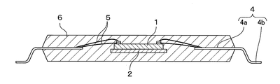
図17は従来の一般的なQFP型半導体装置の断面図、図18は同半導体装置のワイヤボンディング部分の内部構造図である。このQFP型半導体装置は、図17、図18に示すように、集積回路が形成された半導体チップ1がリードフレームのダイパッド部2に搭載されている。また、ダイパッド部2の周辺には放射状にリードフレームのリード4が配置されており、インナーリード4aの先端がダイパッド部2に対して対向している。また、半導体チップ1の表面に形成された電極3とインナーリード4aとがワイヤ5で接続されている。また、半導体チップ1、ワイヤ5、インナーリード4aが一括して樹脂封止体6により樹脂封止され、インナーリード4aに連続したリードフレームのアウターリード4bが樹脂封止体6の外部でガルウィング型に曲げ成形されている。また、図18に示すダイパッドサポート24は、ダイパッド部2をリードフレームに保持する部材である(例えば、非特許文献1参照。)。
FIG. 17 is a cross-sectional view of a conventional general QFP semiconductor device, and FIG. 18 is an internal structure diagram of a wire bonding portion of the semiconductor device. In this QFP type semiconductor device, as shown in FIGS. 17 and 18, a
続いて、従来の一般的なQFP型半導体装置の製造方法について説明する。
まず、金属板で形成されたリードフレームのダイパッド部2に半導体チップ1を搭載する(ダイボンド工程)。なお、リードフレームは、複数個の半導体装置を同時に、あるいは順次形成するために、各半導体装置に対応する矩形のパターンをフレーム枠で連結して複数個、同一平面上の左右方向ないし上下方向に配列したものである。各パターンは、ダイパッド部2を中央に配置し、複数本のリード4の外端部をフレーム枠に接続し、ダイパッド部2をダイパッドサポート24によりフレーム枠に保持する構造である。
Next, a conventional general QFP type semiconductor device manufacturing method will be described.
First, the
次に、半導体チップ1の表面に形成された電極3と、ダイパッド部2の周囲に配置されたインナーリード4aとをワイヤ5で接続する(ワイヤボンディング工程)。次に、半導体チップ1、ダイパッド部2、ワイヤ5、インナーリード4aを一括して封止樹脂で樹脂封止して、樹脂封止体6を形成する(樹脂封止工程)。
Next, the
最後に、アウターリード4bを所定の長さに合わせてフレーム枠から切断して個片に分離するとともに、アウターリード4bを所定の形状に加工して、半導体装置の完成品を得る。
Finally, the
また、ワイヤボンディング方法としては、(1)キャピラリの先端から突出したワイヤの先端に放電によりボールを形成し、(2)熱と超音波を与えながら、そのボールをキャピラリで一方の接続点に押し付けて接続し(ボールボンディング)、(3)キャピラリからワイヤを引き出しながら他方の接続点に移動し、(4)熱と超音波を与えながらキャピラリの先端部でワイヤを他方の接続点にこすり付けて接続する(ウェッジボンディング)、超音波併用熱圧着ボンディング方式が現在の主流であり、一般的には半導体チップの電極側においてボールボンディングを行う。 The wire bonding method is as follows: (1) a ball is formed by discharge at the tip of the wire protruding from the tip of the capillary, and (2) the ball is pressed against one connection point with the capillary while applying heat and ultrasonic waves. (3) Move to the other connection point while pulling out the wire from the capillary, and (4) Rub the wire to the other connection point at the tip of the capillary while applying heat and ultrasonic waves. The connection method (wedge bonding) and the thermocompression bonding method using ultrasonic waves are the mainstream at present, and ball bonding is generally performed on the electrode side of the semiconductor chip.
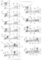
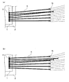
以上のように構成されたQFP型半導体装置において、近年、集積回路の高集積化、高密度化に伴い、多ピン化およびリードの狭ピッチ化が進んできた。しかしながら、多ピン化およびリードの狭ピッチ化が進んできたといってもQFP型半導体装置の外形やピン数は業界で標準化されている。そこで、QFP型半導体装置では、限られたピン数の中で高集積化された半導体チップを保持すべく、電源電極や接地電極などの共通化できる電極をまとめて同一のリードに接続している。図19は同一のインナーリード4aに複数の電極3からのワイヤ5を接続した状態を示す模式図である。図19(a)では同一のインナーリード4aに2本のワイヤ5を接続し、図19(b)では同一のインナーリード4aに3本のワイヤ5を接続している。
以上のように、従来から、QFP型半導体装置においては、電源電極や接地電極などの共通化できる電極をまとめて同一のリードに接続していた。一方、半導体チップ1個当たりの回路規模が飛躍的に大きくなったため、電源電極および接地電極への安定した電流供給を確保するための配線が必要となってきた。反面、半導体組立技術の進歩と低コスト化の要求から、半導体装置の配線材料であるAuワイヤに代表される金属ワイヤは細線化が図られてきた。これらの相反する2つの課題に対し、1個の電極と1本のインナーリードとの接続に複数本のワイヤを使用することが行われている。 As described above, conventionally, in the QFP type semiconductor device, common electrodes such as a power supply electrode and a ground electrode are collectively connected to the same lead. On the other hand, since the circuit scale per semiconductor chip has dramatically increased, wiring for securing a stable current supply to the power supply electrode and the ground electrode has become necessary. On the other hand, metal wires typified by Au wires, which are wiring materials for semiconductor devices, have been made thinner because of advances in semiconductor assembly technology and demands for cost reduction. For these two conflicting problems, the use of a plurality of wires for connecting one electrode and one inner lead has been performed.
しかしながら、通常、ワイヤの十分な接合を行うには一定以上の面積が必要になるため、複数本のワイヤを同一の電極に接続する場合、従来は、電極の面積を、複数本のワイヤをボールボンディングできる大きさにする必要があった。このことがチップ面積の縮小化を阻害していた。 However, since an area of a certain size or more is usually required for sufficient bonding of wires, when connecting a plurality of wires to the same electrode, conventionally, the area of the electrode is reduced to a number of wires. It was necessary to make it large enough for bonding. This hindered the reduction of the chip area.
また、リードフレームのリードや、BGA(ボール・グリッド・アレイ)型半導体装置の配線基板の表層配線に、複数本のワイヤをボールボンディングにより接続する場合もあるが、この場合も同様に、リードまたは表層配線の面積を、複数本のワイヤをボールボンディングできる大きさにする必要があった。このことがパッケージ面積の縮小化を阻害していた。 In some cases, a plurality of wires are connected to the lead of the lead frame or the surface layer wiring of the wiring board of the BGA (Ball Grid Array) type semiconductor device by ball bonding. It was necessary to make the surface layer wiring area large enough to allow ball bonding of a plurality of wires. This hindered the reduction of the package area.
本発明は、上記問題点に鑑み、半導体チップ上の同一の電極又はリードフレームの同一のリードあるいは配線基板上の同一の表層配線に、複数本のワイヤを接続する構造において、電極面積またはパッケージ面積を抑制することができる半導体装置の製造方法、および半導体装置を提供することを目的とする。 In view of the above problems, the present invention provides a structure in which a plurality of wires are connected to the same electrode on a semiconductor chip, the same lead of a lead frame, or the same surface layer wiring on a wiring board. An object of the present invention is to provide a method for manufacturing a semiconductor device and a semiconductor device capable of suppressing the above-described problem.
本発明の請求項1記載の半導体装置の製造方法は、ワイヤ供給装置から突出したワイヤの先端にボールを形成して、そのボールを半導体チップ上の電極に圧着するボールボンディングを行い、その後ワイヤ供給装置を移動させ、接続対象部材にウェッジボンディングを行う第1ボンディング工程と、ワイヤ供給装置から突出したワイヤの先端にボールを形成して、そのボールを、前記第1ボンディング工程においてボールボンディングを行った部分に直上から圧着するボールボンディングを行い、その後ワイヤ供給装置を移動させ、前記第1ボンディング工程における接続対象部材又はその接続対象部材とは異なる接続対象部材にウェッジボンディングを行う第2ボンディング工程と、を具備することを特徴とする。 According to a first aspect of the present invention, there is provided a method of manufacturing a semiconductor device in which a ball is formed at a tip of a wire protruding from a wire supply device, and the ball is bonded to an electrode on a semiconductor chip. A first bonding step of moving the device and performing wedge bonding on the connection target member, and forming a ball at the tip of the wire protruding from the wire supply device, and performing the ball bonding of the ball in the first bonding step A second bonding step in which ball bonding is performed to directly press onto the portion, and then the wire supply device is moved, and the bonding target member in the first bonding step or wedge bonding is performed on a connection target member different from the connection target member; It is characterized by comprising.
また、本発明の請求項2記載の半導体装置の製造方法は、請求項1記載の半導体装置の製造方法であって、前記第2ボンディング工程を2回以上繰り返し行い、前記電極に複数本のワイヤを接続させることを特徴とする。
A method for manufacturing a semiconductor device according to
また、本発明の請求項3記載の半導体装置の製造方法は、請求項2記載の半導体装置の製造方法であって、繰り返し行う前記第2ボンディング工程に際し、前記第1ボンディング工程における接続対象部材に少なくとも1本のワイヤをウェッジボンディングにより接続させることを特徴とする。 According to a third aspect of the present invention, there is provided a method for manufacturing a semiconductor device according to the second aspect of the present invention, wherein the connection target member in the first bonding step is used when the second bonding step is repeatedly performed. At least one wire is connected by wedge bonding.
また、本発明の請求項4記載の半導体装置の製造方法は、請求項2記載の半導体装置の製造方法であって、繰り返し行う前記第2ボンディング工程に際し、前記第1ボンディング工程における接続対象部材とは異なる同一の接続対象部材に少なくとも2本のワイヤをウェッジボンディングにより接続させることを特徴とする。 According to a fourth aspect of the present invention, there is provided a method of manufacturing a semiconductor device according to the second aspect of the present invention, wherein, in the second bonding step that is repeatedly performed, the connection target member in the first bonding step and Is characterized in that at least two wires are connected to different same connection target members by wedge bonding.
また、本発明の請求項5記載の半導体装置の製造方法は、請求項1記載の半導体装置の製造方法であって、ワイヤ供給装置から突出したワイヤの先端にボールを形成し、そのボールを、前記第1ボンディング工程ないし前記第2ボンディング工程においてウェッジボンディングを行う部分に圧着してバンプを形成するバンプ形成工程を具備し、前記第1ボンディング工程ないし前記第2ボンディング工程に際し、前記バンプにウェッジボンディングを行うことを特徴とする。
A method for manufacturing a semiconductor device according to
また、本発明の請求項6記載の半導体装置の製造方法は、ワイヤ供給装置から突出したワイヤの先端にボールを形成して、そのボールを半導体チップの周囲に配置されたリードあるいは配線部材に圧着するボールボンディングを行い、その後ワイヤ供給装置を移動させ、接続対象部材にウェッジボンディングを行う第1ボンディング工程と、ワイヤ供給装置から突出したワイヤの先端にボールを形成して、そのボールを、前記第1ボンディング工程においてボールボンディングを行った部分に直上から圧着するボールボンディングを行い、その後ワイヤ供給装置を移動させ、前記第1ボンディング工程における接続対象部材又はその接続対象部材とは異なる接続対象部材にウェッジボンディングを行う第2ボンディング工程と、を具備することを特徴とする。 According to a sixth aspect of the present invention, there is provided a method of manufacturing a semiconductor device, wherein a ball is formed at a tip of a wire protruding from a wire supply device, and the ball is crimped to a lead or a wiring member disposed around the semiconductor chip. Performing a ball bonding, and then moving the wire supply device to perform wedge bonding on the connection target member; forming a ball at the tip of the wire protruding from the wire supply device; Ball bonding is performed by directly pressing onto the portion where ball bonding has been performed in one bonding process, and then the wire supply device is moved so that the connection target member in the first bonding process or a connection target member different from the connection target member is wedged. A second bonding step for performing bonding. The features.
また、本発明の請求項7記載の半導体装置の製造方法は、請求項6記載の半導体装置の製造方法であって、前記第2ボンディング工程を2回以上繰り返し行い、前記リードあるいは前記配線部材に複数本のワイヤを接続させることを特徴とする。 According to a seventh aspect of the present invention, there is provided a method for manufacturing a semiconductor device according to the sixth aspect, wherein the second bonding step is repeated twice or more to form the lead or the wiring member. A plurality of wires are connected.
また、本発明の請求項8記載の半導体装置の製造方法は、請求項7記載の半導体装置の製造方法であって、繰り返し行う前記第2ボンディング工程に際し、前記第1ボンディング工程における接続対象部材に少なくとも1本のワイヤをウェッジボンディングにより接続させることを特徴とする。
Further, the method for manufacturing a semiconductor device according to claim 8 of the present invention is the method for manufacturing a semiconductor device according to
また、本発明の請求項9記載の半導体装置の製造方法は、請求項7記載の半導体装置の製造方法であって、繰り返し行う前記第2ボンディング工程に際し、前記第1ボンディング工程における接続対象部材とは異なる同一の接続対象部材に少なくとも2本のワイヤをウェッジボンディングにより接続させることを特徴とする。
A method for manufacturing a semiconductor device according to
また、本発明の請求項10記載の半導体装置の製造方法は、請求項6記載の半導体装置の製造方法であって、ワイヤ供給装置から突出したワイヤの先端にボールを形成し、そのボールを、前記第1ボンディング工程ないし前記第2ボンディング工程においてウェッジボンディングを行う部分に圧着してバンプを形成するバンプ形成工程を具備し、前記第1ボンディング工程ないし前記第2ボンディング工程に際し、前記バンプにウェッジボンディングを行うことを特徴とする。
A method for manufacturing a semiconductor device according to
また、本発明の請求項11記載の半導体装置は、電極を有する半導体チップと、前記半導体チップが搭載されるチップ搭載部と、前記チップ搭載部の周囲に配置されるリード又は配線部材と、前記半導体チップが有する前記電極と前記リード又は配線部材とを接続するワイヤと、を備え、少なくとも前記半導体チップ、前記チップ搭載部、前記ワイヤおよび前記リード又は配線部材の前記ワイヤとの接続部分が樹脂封止された半導体装置であって、前記半導体チップが有する前記電極のうちの少なくとも1個に、複数本の前記ワイヤの一端の接続部が重ねて接続されており、それらの接続部はボールボンディング法特有の、厚みのあるコイン状に押しつぶされた突起部のほぼ中央からワイヤが導出される形状に形成されていることを特徴とする。 A semiconductor device according to claim 11 of the present invention is a semiconductor chip having electrodes, a chip mounting portion on which the semiconductor chip is mounted, a lead or wiring member disposed around the chip mounting portion, A wire for connecting the electrode of the semiconductor chip and the lead or the wiring member, and at least a connection portion of the semiconductor chip, the chip mounting portion, the wire and the wire of the lead or the wiring member is sealed with resin. A semiconductor device that is stopped, wherein at least one of the electrodes of the semiconductor chip is connected to a connecting portion of one end of the plurality of wires in an overlapping manner, and the connecting portion is connected by a ball bonding method. It is characterized in that the wire is led out from the approximate center of the peculiar, thick coin-shaped protrusion. .
また、本発明の請求項12記載の半導体装置は、請求項11記載の半導体装置であって、前記半導体チップが有する前記電極に一端が重ねて接続された複数本の前記ワイヤのうちの少なくとも一部は、その他端が、同一の前記リード又は配線部材に、ウェッジボンディング法特有の厚みの無い三日月状または楕円状の形状をなして接続されていることを特徴とする。 A semiconductor device according to a twelfth aspect of the present invention is the semiconductor device according to the eleventh aspect, wherein at least one of the plurality of wires connected at one end to the electrode of the semiconductor chip. The other end of the part is connected to the same lead or wiring member in the shape of a crescent or ellipse having no thickness peculiar to the wedge bonding method.
また、本発明の請求項13記載の半導体装置は、請求項11記載の半導体装置であって、前記半導体チップを複数個備え、少なくとも1箇の前記半導体チップが有する少なくとも1箇の前記電極に一端が重ねて接続された複数本の前記ワイヤのうちの少なくとも一部は、その他端が、他方の前記半導体チップが有する電極に、ウェッジボンディング法特有の厚みの無い三日月状または楕円状の形状をなして接続されていることを特徴とする。 A semiconductor device according to a thirteenth aspect of the present invention is the semiconductor device according to the eleventh aspect, comprising a plurality of the semiconductor chips, and one end of at least one of the electrodes of the at least one semiconductor chip. At least a part of the plurality of wires connected in a stacked manner has a crescent shape or an ellipse shape with no other thickness on the electrode of the other semiconductor chip at the other end. And are connected.
また、本発明の請求項14記載の半導体装置は、請求項11記載の半導体装置であって、前記半導体チップを複数個備え、少なくとも1箇の前記半導体チップが有する少なくとも1箇の前記電極に一端が重ねて接続された複数本の前記ワイヤの一部は、その他端が、他方の前記半導体チップが有する電極に、ウェッジボンディング法特有の厚みの無い三日月状または楕円状の形状をなして接続され、他の一部は、その他端が、前記リード又は配線部材に、ウェッジボンディング法特有の厚みの無い三日月状または楕円状の形状をなして接続されていることを特徴とする。 A semiconductor device according to a fourteenth aspect of the present invention is the semiconductor device according to the eleventh aspect, comprising a plurality of the semiconductor chips, and one end of at least one electrode of the at least one semiconductor chip. A part of the plurality of wires connected to each other is connected at the other end to the electrode of the other semiconductor chip in a crescent or elliptical shape having no thickness peculiar to the wedge bonding method. The other part is characterized in that the other end is connected to the lead or the wiring member in the shape of a crescent or ellipse having no thickness peculiar to the wedge bonding method.
また、本発明の請求項15記載の半導体装置は、請求項11記載の半導体装置であって、前記チップ搭載部および前記リードは、金属板を加工して製作されるリードフレームの構成部材であることを特徴とする。 A semiconductor device according to a fifteenth aspect of the present invention is the semiconductor device according to the eleventh aspect, wherein the chip mounting portion and the lead are constituent members of a lead frame manufactured by processing a metal plate. It is characterized by that.
また、本発明の請求項16記載の半導体装置は、請求項11記載の半導体装置であって、前記チップ搭載部および前記配線部材は、配線基板の構成部材であることを特徴とする。 According to a sixteenth aspect of the present invention, there is provided the semiconductor device according to the eleventh aspect, wherein the chip mounting portion and the wiring member are constituent members of a wiring board.
また、本発明の請求項17記載の半導体装置は、電極を有する半導体チップと、前記半導体チップが搭載されるチップ搭載部と、前記チップ搭載部の周囲に配置されるリード又は配線部材と、前記半導体チップが有する前記電極と前記リード又は配線部材とを接続するワイヤと、を備え、少なくとも前記半導体チップ、前記チップ搭載部、前記ワイヤおよび前記リード又は配線部材の前記ワイヤとの接続部分が樹脂封止された半導体装置であって、前記リード又は配線部材のうちの少なくとも1個に、複数本の前記ワイヤの一端の接続部が重ねて接続されており、それらの接続部はボールボンディング法特有の、厚みのあるコイン状に押しつぶされた突起部のほぼ中央からワイヤが導出される形状に形成されていることを特徴とする。 A semiconductor device according to claim 17 of the present invention is a semiconductor chip having electrodes, a chip mounting portion on which the semiconductor chip is mounted, a lead or wiring member disposed around the chip mounting portion, A wire for connecting the electrode of the semiconductor chip and the lead or the wiring member, and at least a connection portion of the semiconductor chip, the chip mounting portion, the wire and the wire of the lead or the wiring member is sealed with resin. A semiconductor device that is stopped, wherein at least one of the leads or wiring members is connected to a connecting portion of one end of a plurality of the wires, and these connecting portions are specific to the ball bonding method. The wire is led out from substantially the center of the protruding portion crushed into a thick coin shape.
また、本発明の請求項18記載の半導体装置は、請求項17記載の半導体装置であって、前記リード又は配線部材に一端が重ねて接続された複数本の前記ワイヤの一部は、その他端が他方の前記リード又は配線部材に、ウェッジボンディング法特有の、厚みの無い三日月状または楕円状の形状をなして接続され、他の一部は、その他端が前記半導体チップが有する前記電極に、ウェッジボンディング法特有の、先端が厚みの無い三日月状または楕円状の形状をなして接続されていることを特徴とする。
The semiconductor device according to claim 18 of the present invention is the semiconductor device according to
また、本発明の請求項19記載の半導体装置は、請求項17記載の半導体装置であって、前記半導体チップを複数個備え、前記リード又は配線部材に一端が重ねて接続された複数本の前記ワイヤのうちの少なくとも一部は、その他端が互いに異なる前記半導体チップの各々が有する前記電極に、ウェッジボンディング法特有の厚みの無い三日月状または楕円状の形状をなして接続されていることを特徴とする。
The semiconductor device according to claim 19 of the present invention is the semiconductor device according to
また、本発明の請求項20記載の半導体装置は、請求項17記載の半導体装置であって、前記チップ搭載部および前記リードは、金属板を加工して製作されるリードフレームの構成部材であることを特徴とする。 A semiconductor device according to a twentieth aspect of the present invention is the semiconductor device according to the seventeenth aspect, wherein the chip mounting portion and the lead are constituent members of a lead frame manufactured by processing a metal plate. It is characterized by that.
また、本発明の請求項21記載の半導体装置は、請求項17記載の半導体装置であって、前記チップ搭載部および前記配線部材は、配線基板の構成部材であることを特徴とする。 A semiconductor device according to a twenty-first aspect of the present invention is the semiconductor device according to the seventeenth aspect, wherein the chip mounting portion and the wiring member are constituent members of a wiring board.
本発明の好ましい形態によれば、半導体チップ上の同一の電極に対して、電極の面積を拡大することなく2本以上のワイヤを接続することができる。よって、半導体チップ上の同一の電極に複数本のワイヤを接続する構造において、接続するワイヤ数にかかわらず常に電極の面積を最小にすることができ、チップ全体に占める電極の個数および面積を最小にすることが可能となる。通常、半導体チップにおいては、その外周部に電極が一列ないし複数列に配置されており、電極の個数および面積を最小にすることでチップサイズを小さくすることができる。また、複数本のワイヤを同一の電極に接続できるので、より細線化されたワイヤを用いながら、電源電極や接地電極への安定した電流容量を確保すると同時に、半導体チップの小型化を実現できるので、小型、高品質の半導体装置を安価に提供できるようになる。 According to the preferred embodiment of the present invention, two or more wires can be connected to the same electrode on the semiconductor chip without increasing the area of the electrode. Therefore, in the structure in which multiple wires are connected to the same electrode on the semiconductor chip, the area of the electrode can always be minimized regardless of the number of wires to be connected, and the number and area of the electrodes in the entire chip can be minimized. It becomes possible to. Usually, in a semiconductor chip, electrodes are arranged in one or more rows on the outer periphery thereof, and the chip size can be reduced by minimizing the number and area of the electrodes. In addition, since multiple wires can be connected to the same electrode, it is possible to reduce the size of the semiconductor chip while securing a stable current capacity to the power supply electrode and the ground electrode while using a finer wire. Therefore, a small-sized and high-quality semiconductor device can be provided at low cost.
また、近年、機器の小型化の要求から1個の半導体装置(パッケージ)の中に複数個の半導体チップを内蔵することが行われてきており、QFP型の半導体装置では、各半導体チップ上の電極とリード(インナーリード)とをワイヤで接続すると共に、互いに異なる半導体チップ上の電極同士をワイヤで接続することが行われるようになってきた。同様に、配線基板を用いたBGA(ボール・グリッド・アレイ)型の半導体装置においても、1個のパッケージの中に複数個の半導体チップを内蔵して、各半導体チップ上の電極と配線基板上の表層配線(配線部材)とをワイヤで接続すると共に、互いに異なる半導体チップ上の電極同士をワイヤで接続することが行われるようになってきた。 In recent years, a plurality of semiconductor chips have been built in one semiconductor device (package) due to a demand for miniaturization of equipment. In a QFP type semiconductor device, each semiconductor chip has a built-in structure. An electrode and a lead (inner lead) are connected by a wire, and electrodes on different semiconductor chips are connected by a wire. Similarly, in a BGA (ball grid array) type semiconductor device using a wiring board, a plurality of semiconductor chips are built in one package, and electrodes on each semiconductor chip and the wiring board are mounted. In addition to connecting the surface layer wiring (wiring member) with wires, electrodes on different semiconductor chips have been connected with wires.
本発明の好ましい形態によれば、同一の電極からの複数本のワイヤをそれぞれ異なるリード(インナーリード)又は配線部材(配線基板の表層配線)に接続することや、同一の電極からの複数本のワイヤを互いに異なる半導体チップ上の電極同士の接続に用いることも可能となるため、チップサイズを大きくすることなく、複数本のワイヤが接続された電極を、例えば他方の半導体チップ上の電極とリードとの中継電極として使用することができるようになる。また、同一のリード(インナーリード)又は配線部材(配線基板の表層配線)からの複数本のワイヤをそれぞれ異なるリード又は配線部材に接続することや、同一のリード又は配線部材からの複数本のワイヤをそれぞれ異なる半導体チップ上の電極に接続することや、同一のリード又は配線部材からの複数本のワイヤをそれぞれ半導体チップ上の異なる電極に接続することが可能となるため、リードを大きくすることなく、すなわちパッケージを大きくすることなく、複数本のワイヤが接続されたリード又は配線部材を、例えば各半導体チップ上の複数の電極の電源として用いたり、互いに異なる半導体チップ上の電極同士の中継リード又は中継配線として使用することができるようになる。したがって、装置内の配線を簡略化することが可能となり、高集積、高密度、高品質な半導体装置をコンパクトかつ安価に提供できるようになる。 According to a preferred embodiment of the present invention, a plurality of wires from the same electrode are connected to different leads (inner leads) or wiring members (surface layer wiring of a wiring board), or a plurality of wires from the same electrode are connected. Since wires can be used to connect electrodes on different semiconductor chips, an electrode to which a plurality of wires are connected can be connected to, for example, an electrode on the other semiconductor chip without increasing the chip size. And can be used as a relay electrode. Also, a plurality of wires from the same lead (inner lead) or wiring member (surface wiring of the wiring board) are connected to different leads or wiring members, or a plurality of wires from the same lead or wiring member. Can be connected to electrodes on different semiconductor chips, and a plurality of wires from the same lead or wiring member can be connected to different electrodes on the semiconductor chip without increasing the leads. That is, without using a large package, a lead or a wiring member to which a plurality of wires are connected is used as a power source for a plurality of electrodes on each semiconductor chip, for example, or a relay lead between electrodes on different semiconductor chips or It can be used as a relay wiring. Therefore, the wiring in the device can be simplified, and a highly integrated, high-density, high-quality semiconductor device can be provided in a compact and inexpensive manner.
(実施の形態1)
以下、本発明の実施の形態1について、図面を参照しながら説明する。
図1は本発明の実施の形態1に係る半導体装置の断面図、図2(a)は同半導体装置のワイヤボンディング部分の内部構造を説明するための斜視図、図2(b)は同半導体装置のワイヤボンディング部分の内部構造を説明するための上面図、図2(c)は同半導体装置のワイヤボンディング部分の内部構造を説明するための断面図である。なお、以下の説明において同一の部材には同一符号を付して、適宜説明を省略する。
(Embodiment 1)
1 is a cross-sectional view of a semiconductor device according to
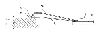
この半導体装置はQFP型の半導体装置であり、図1に示すように、集積回路が形成された半導体チップ1がリードフレームのダイパッド部(チップ搭載部)2に搭載されている。また、ダイパッド部2の周辺には放射状にリードフレームのリード4が配置されており、インナーリード4aの先端がダイパッド部2に対して対向している。また、半導体チップ1の表面に形成されている電極3とインナーリード4aとがワイヤ5で接続されている。また、半導体チップ1、ダイパッド部2、ワイヤ5、インナーリード4a(リード4のワイヤ接続部分)が一括して樹脂封止体6により樹脂封止され、インナーリード4aに連続したリードフレームのアウターリード4bが樹脂封止体6の外部でガルウィング型に曲げ成形されている。
This semiconductor device is a QFP type semiconductor device. As shown in FIG. 1, a
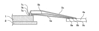
この半導体装置が従来のものと異なるのは、図2に示すように、半導体チップ1上の少なくとも1個の電極3に2本のワイヤ5a、5bの一端の接続部が重ねて接続されており、それらの接続部が、ボールボンディング法特有の、厚みのあるコイン状に押しつぶされた突起部のほぼ中央からワイヤが導出される形状に形成されている点と、それらの2本のワイヤ5a、5bの他端が、同一のインナーリード4aに、ウェッジボンディング法特有の厚みの無い三日月状または楕円状の形状をなして接続されている点である。
As shown in FIG. 2, this semiconductor device is different from the conventional one in that a connection portion at one end of two
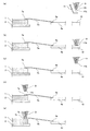
続いて、同一の電極に2本のワイヤを接続する方法について、図3に示す工程断面図に沿って説明する。まず、図3(a)に示すように、ワイヤ供給装置であるキャピラリ9の先端から突出したワイヤ5aの先端とトーチ10との間で放電を行い、スパークによりボール11aを形成する。
Next, a method of connecting two wires to the same electrode will be described along the process cross-sectional view shown in FIG. First, as shown in FIG. 3A, electric discharge is performed between the tip of the
次に図3(b)〜図3(d)に示すように、半導体チップ1上の電極にボール11aを圧着して(ボールボンディング)、ボールボンディング側の接続部7aを形成する。その後、図3(e)〜図3(g)に示すように、ワイヤ5aを水平方向に折り曲げて引き出し、ワイヤ5aが所定の軌跡に沿って配線されるようにキャピラリ9を移動させ、接続対象部材であるインナーリード4aにワイヤ5aをこすり付けて(ウェッジボンディング)、ウェッジボンディング側の接続部8aを形成する。
Next, as shown in FIGS. 3B to 3D, a
以上の第1ボンディング工程を行った後、第2ボンディング工程を行う。すなわち、まず、図3(h)に示すように、キャピラリ9の先端から突出したワイヤ5bの先端とトーチ10との間で放電を行い、スパークによりボール11bを形成する。
After performing the first bonding step, the second bonding step is performed. That is, first, as shown in FIG. 3 (h), discharge is performed between the tip of the
次に図3(i)に示すように、接続部7a(第1ボンディング工程においてボールボンディングを行った部分)に直上からボール11bを圧着して(ボールボンディング)、ボールボンディング側の接続部7bを形成する。その後、図3(j)〜図3(l)に示すように、ワイヤ5bを垂直方向に引き出して折り曲げ、ワイヤ5bが所定の軌跡に沿って配線されるようにキャピラリ9を移動させ、接続対象部材であるインナーリード4aにワイヤ5bをこすり付けて(ウェッジボンディング)、ウェッジボンディング側の接続部8bを形成する。なお、ここでは、第1ボンディング工程と第2ボンディング工程における接続対象部材は同一のインナーリード4aである。
Next, as shown in FIG. 3 (i), the
以上のように第1および第2ボンディング工程を行うことで、同一の電極に2本のワイヤの一端をボールボンディング法により重ねて接続することができる。ワイヤボンディング工程で使用するワイヤには、一般的に、金や銅等の金属を原料とする直径φ15〜40μmのものが使われる。ボールボンディング法においてワイヤの一端に形成されるボールの直径はワイヤの直径の1.5倍〜4倍程度であり、接続点に接合されるときキャピラリの先端部で厚さが5〜60μm程度になるまで押しつぶされるので、ボールボンディング側の接続部は、厚みのあるコイン状に押しつぶされた突起部のほぼ中央からワイヤが導出される形状になる。一方、ワイヤの他端は、キャピラリの先端周辺部で接続点にこすり付けるように潰すので、ウェッジボンディング側の接続部は、厚みの無い三日月状または楕円状の形状になる。 By performing the first and second bonding steps as described above, one end of two wires can be overlapped and connected to the same electrode by the ball bonding method. As a wire used in the wire bonding process, generally, a wire having a diameter of 15 to 40 μm made of a metal such as gold or copper is used. In the ball bonding method, the diameter of the ball formed at one end of the wire is about 1.5 to 4 times the diameter of the wire, and the thickness at the tip of the capillary is about 5 to 60 μm when bonded to the connection point. As a result, the connecting portion on the ball bonding side has a shape in which the wire is led out from substantially the center of the protruding portion crushed into a thick coin shape. On the other hand, the other end of the wire is crushed so as to be rubbed against the connection point around the tip of the capillary, so that the connection part on the wedge bonding side has a crescent or elliptical shape with no thickness.
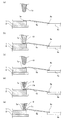
また、例えば図3(g)に示すように、ボールボンディング側の接続部7aの上部にはワイヤ5aの一部が存在しているため、その上から圧着するボール11bとの接続ズレを防止するために、キャピラリ9によってボール11bを確実に保持しておく必要がある。これに対して、以下で説明する方法を実施すれば、容易に接続ズレを防止することができる。図4は、同一の電極に複数本のワイヤを重ねて接続するに際して接続ズレを防止する方法を説明するための工程断面図である。
Further, for example, as shown in FIG. 3G, since a part of the
まず、第1ボンディング工程後、図4(a)に示すように、キャピラリ9の先端から突出したワイヤ5bの先端とトーチ10との間で放電を行い、スパークによりボール11bを形成する。次に図4(b)に示すように、平坦部12上にボール11bを押し付けて、ボール11bの下面に平坦面を形成する。次に図4(c)〜図4(d)に示すように、接続部7aに直上からボール11bを圧着してボールボンディング側の接続部7bを形成する。
First, after a 1st bonding process, as shown to Fig.4 (a), it discharges between the front-end | tip of the
このように、第2ボンディング工程に際し、キャピラリ9から突出したワイヤ5bの先端にボール11bを形成した後、平坦部12にボール11bを押し付け、ボール11bの下面に平坦面を形成してボールボンディングを行う。
Thus, in the second bonding step, after forming the
この方法によれば、ボール11bの下面を平坦面としたので、接続部7aの上部に存在するワイヤ5aと接触しても接触ズレを防止することができ、確実な接合を実現できる。なお、平坦部12としては、例えばリードフレームの一部やワイヤボンド設備の一部の平坦面を用いることができる。また、後述するように本発明をBGA型の半導体装置に適用する場合には、配線基板の一部の平坦面を用いることができる。
According to this method, since the lower surface of the
また、以下で説明する方法により接続ズレを防止してもよい。すなわち、図5(a)〜図5(c)に示すように、第1ボンディング工程後、まず、接続部7aに直上から、先端が円錐型の突起形状をしている加圧ツール13を押し当てて接続部7aを押し潰す。次に、図5(d)、図5(e)に示すように、押し潰した接続部7aに直上からボール11bを圧着してボールボンディング側の接続部7bを形成する。加圧ツール13の先端部が押し当てられた接続部7aの上部には円錐型の窪みができるため、ボール11bは確実にその窪みの中央に位置合わせされる。これにより更に確実な接合を実現できる。なお、加圧ツール13の先端部の円錐の開き角度は120〜170°の鈍角に設定するのが望ましい。
Further, the connection shift may be prevented by the method described below. That is, as shown in FIG. 5A to FIG. 5C, after the first bonding step, first, the
このように、第2ボンディング工程においてボールボンディングを行う部分(接続部7a)に直上から加圧ツールを押し当てて該部分(接続部7a)を押し潰す工程をさらに含み、第2ボンディング工程に際し、その押し潰した部分にボールボンディングを行う。
As described above, the method further includes a step of pressing the pressure tool from directly above the portion (connecting
また、以下で説明する方法により接続ズレを防止してもよい。この方法は、加圧ツールの先端が球面型の突起形状をしている点のみが、上記した方法と異なる。すなわち、図6(a)〜図6(c)に示すように、第1ボンディング工程後、まず、接続部7aに直上から、先端が球面型の突起形状をしている加圧ツール14を押し当てて接続部7aを押し潰す。次に、図6(d)、図6(e)に示すように、押し潰した接続部7aに直上からボール11bを圧着してボールボンディング側の接続部7bを形成する。加圧ツール13の先端部が押し当てられた接続部7aの上部には球面型の窪みができ、接続部7aにボール11bを圧着する際に、まず、その窪みの中心部とボール11bが点接触するので、確実に位置合わせすることができる。また、窪みを球面型にすることで、空隙のない確実な接合を実現できる。なお、加圧ツール14の先端部の球面の半径はボール11bの半径の1.5〜5倍の範囲で設定することが望ましい。
Further, the connection shift may be prevented by the method described below. This method differs from the above-described method only in that the tip of the pressing tool has a spherical protrusion shape. That is, as shown in FIG. 6A to FIG. 6C, after the first bonding step, first, the
以上説明した方法によれば、ボールボンディング法によって形成した接続部上に、さらに他のワイヤの一端をボールボンディング法によって接続するに際し、接触ズレを防止することができる。 According to the method described above, contact misalignment can be prevented when one end of another wire is connected to the connecting portion formed by the ball bonding method by the ball bonding method.
なお、本実施の形態1では、同一の電極からの複数本のワイヤを同一のインナーリードに接続する場合について説明したが、それらのワイヤをそれぞれ異なるインナーリードに接続してもよい。 In the first embodiment, the case where a plurality of wires from the same electrode are connected to the same inner lead has been described. However, these wires may be connected to different inner leads.
(実施の形態2)
続いて、本発明の実施の形態2について、図面を参照しながら説明する。図7は本発明の実施の形態2に係る半導体装置のワイヤボンディング部分の内部構造を説明するための断面図である。但し、前述した実施の形態1にて説明した部材と同一の部材には同一符号を付して、説明を省略する。
(Embodiment 2)
Next,
この半導体装置は、半導体チップ上の少なくとも1個の電極に3本のワイヤの一端がボールボンディング法により重ねて接続され、その3本のワイヤ5の他端が同一のインナーリード上の異なる位置にウェッジボンディング法により接続されている点が、前述した実施の形態1と異なる。すなわち、図7に示すように、半導体チップ1上の同一の電極には、ワイヤ5a〜5cのボールボンディング側の接続部7a〜7cが重ねて形成されている。また、同一のインナーリード4a上の異なる位置に、ワイヤ5a〜5cのウェッジボンディング側の接続部8a〜8cが形成されている。この接続は、実施の形態1で説明した第2ボンディング工程を2回繰り返すことで実現できる。この構成により、必要に応じて電流容量を調整することが可能となり、更に小型・高品質で低コストな半導体装置を提供することが可能となる。
In this semiconductor device, one end of three wires is overlapped and connected to at least one electrode on a semiconductor chip by a ball bonding method, and the other ends of the three
なお、本実施の形態2では、同一の電極に3本のワイヤを接続する場合について説明したが、第2ボンディング工程を2回以上繰り返すことで、同一の電極に3本以上のワイヤを接続することが出来る。 In the second embodiment, the case where three wires are connected to the same electrode has been described. However, by repeating the second bonding step twice or more, three or more wires are connected to the same electrode. I can do it.
(実施の形態3)
続いて、本発明の実施の形態3について、図面を参照しながら説明する。図8は本発明の実施の形態3に係る半導体装置のワイヤボンディング部分の内部構造を説明するための断面図である。但し、前述した実施の形態1、2にて説明した部材と同一の部材には同一符号を付して、説明を省略する。
(Embodiment 3)
Subsequently,
この半導体装置は、半導体チップ上の少なくとも1個の電極に2本のワイヤの一端がボールボンディング法により重ねて接続され、その2本のワイヤの他端が、同一のインナーリード上の同一の接続点に、バンプを介して、ウェッジボンディング法により重ねて接続されている点が、前述した実施の形態1と異なる。 In this semiconductor device, one end of two wires is overlapped and connected to at least one electrode on a semiconductor chip by a ball bonding method, and the other end of the two wires is connected to the same inner lead. This is different from the first embodiment described above in that the bumps are overlapped and connected by the wedge bonding method.
すなわち、図8に示すように、ワイヤ5aのウェッジボンディング側の接続部上にバンプ15を形成し、そのバンプ15上に、ワイヤ5bのウェッジボンディング側の接続部を形成した構成となっている。このバンプ15は、キャピラリから突出したワイヤの先端にボールを形成し、そのボールを、第2ボンディング工程においてウェッジボンディングを行う部分に圧着することで形成することができる。よって、このバンプ形成工程を、ワイヤ5bのウェッジボンディングを行う前に実行しておき、第2ボンディング工程に際し、そのバンプ15上にウェッジボンディングを行うことで、バンプ15上にワイヤ5bのウェッジボンディング側の接続部を形成することができる。
That is, as shown in FIG. 8, the
本実施の形態3によれば、ボールボンディング側とウェッジボンディング側の両方において、従来、1本のワイヤしか接続することができなかった面積に複数本のワイヤを接続することが可能となり、半導体チップの縮小化と共にリードフレームの縮小化が可能となる。よって、配線の自由度が向上し、半導体装置の小型化に大きく寄与する。また、ウェッジボンディング法によって形成された接続部は前述したように厚みの無い三日月状または楕円状の形状であるので、これをそのまま垂直に重ねてボンディングする場合は各々のワイヤの接続状態を安定化することが重要である。これに対し、本実施の形態3のように、バンプを形成し、そのバンプ上にウェッジボンディングを行えば、ウェッジボンディングにより積み重ねられた各ワイヤの接続部はバンプを介し強固に接合されることになるので、接合信頼性の向上を実現することができる。 According to the third embodiment, on both the ball bonding side and the wedge bonding side, it is possible to connect a plurality of wires to an area where conventionally only one wire can be connected. As a result, the lead frame can be reduced. Therefore, the degree of freedom of wiring is improved, which greatly contributes to downsizing of the semiconductor device. In addition, since the connection part formed by the wedge bonding method has a crescent or elliptical shape with no thickness as described above, the connection state of each wire is stabilized when bonding it vertically as it is. It is important to. On the other hand, if the bump is formed and wedge bonding is performed on the bump as in the third embodiment, the connecting portions of the wires stacked by the wedge bonding are firmly bonded via the bump. Therefore, it is possible to improve the bonding reliability.
なお、本実施の形態3では、ウェッジボンディング側の接続部を2つ重ねて接続する場合について説明したが、上記したバンプ形成工程を繰り返して、先に形成した接続部上にバンプを形成することで、ウェッジボンディング側の接続部を3つ以上重ねて接続することもできる。
In addition, in this
(実施の形態4)
続いて、本発明の実施の形態4について、図面を参照しながら説明する。図9(a)は本発明の実施の形態4に係る半導体装置のワイヤボンディング部分の内部構造を説明するための上面図、図9(b)は同半導体装置のワイヤボンディング部分の内部構造を説明するための断面図である。但し、前述した実施の形態1〜3にて説明した部材と同一の部材には同一符号を付して、説明を省略する。
(Embodiment 4)
Next, a fourth embodiment of the present invention will be described with reference to the drawings. FIG. 9A is a top view for explaining the internal structure of the wire bonding portion of the semiconductor device according to the fourth embodiment of the present invention, and FIG. 9B shows the internal structure of the wire bonding portion of the semiconductor device. It is sectional drawing for doing. However, the same members as those described in the first to third embodiments are denoted by the same reference numerals, and description thereof is omitted.
この半導体装置は、垂直方向に積層された2個の半導体チップがダイパッド部に搭載されており、同一の電極からの複数本のワイヤがそれぞれ異なる接続対象部材に接続されている点が、前述した実施の形態1〜3と異なる。 In this semiconductor device, two semiconductor chips stacked in the vertical direction are mounted on the die pad portion, and a plurality of wires from the same electrode are connected to different connection target members as described above. Different from the first to third embodiments.
すなわち、図9に示すように、上方の半導体チップ1a上の同一の電極3aに2本のワイヤ5a、5bの一端がボールボンディング法により重ねて接続されており、ワイヤ5aの他端は、下方の半導体チップ1b上の電極3bにウェッジボンディング法により接続され、ワイヤ5bの他端は、インナーリード4aにウェッジボンディング法により接続されている。
That is, as shown in FIG. 9, one end of two
また、ここでは、キャピラリから突出したワイヤの先端にボールを形成し、そのボールを、第1ボンディング工程においてウェッジボンディングを行う部分(電極3b)に圧着してバンプ15を形成するバンプ形成工程を、ワイヤ5aのウェッジボンディングを行う前に実行しておき、バンプ15上にワイヤ5aのウェッジボンディング側の接続部8aを形成している。
Further, here, a bump forming step of forming a
また、図10に示すように、下方の半導体チップ上の同一の電極に2本のワイヤを接続してもよい。すなわち、図10に示す半導体装置では、下方の半導体チップ1b上の同一の電極3bに2本のワイヤ5a、5bの一端がボールボンディング法により重ねて接続されており、ワイヤ5aの他端は、インナーリード4aにウェッジボンディング法により接続され、ワイヤ5bの他端は、上方の半導体チップ1a上の電極3aにウェッジボンディング法により接続されている。
Further, as shown in FIG. 10, two wires may be connected to the same electrode on the lower semiconductor chip. That is, in the semiconductor device shown in FIG. 10, one end of two
また、ここでは、キャピラリから突出したワイヤの先端にボールを形成し、そのボールを、第2ボンディング工程においてウェッジボンディングを行う部分(電極3a)に圧着してバンプ15を形成するバンプ形成工程を、ワイヤ5bのウェッジボンディングを行う前に実行しておき、バンプ15上にワイヤ5bのウェッジボンディング側の接続部8bを形成している。
Further, here, a bump forming step is performed in which a ball is formed at the tip of the wire protruding from the capillary, and the ball is crimped to a portion (
なお、半導体チップ上の同一の電極に2本のワイヤを重ねて接続する場合について説明したが、無論、同一の電極に3本以上のワイヤを重ねて接続することもできる。また、同一の電極からの2本のワイヤのうちの一方を他の半導体チップ上の電極に接続し、他方をインナーリードに接続したが、この接続形態に限定されるものではなく、同一の電極からの複数本のワイヤ各々のウェッジボンディング側の接続対象部材は、他の半導体チップ上の同一の電極であってもよいし、他の半導体チップ上の異なる電極であってもよいし、同一のインナーリードであってもよいし、異なるインナーリードであってもよい。また、ウェッジボンディング側の接続対象部材が同一の場合、実施の形態3において説明したようにランドを形成することで、ウェッジボンディング側の接続部を同一の接続点に重ねて接続してもよい。 Although the case where two wires are overlapped and connected to the same electrode on the semiconductor chip has been described, of course, three or more wires can be overlapped and connected to the same electrode. In addition, one of the two wires from the same electrode is connected to an electrode on another semiconductor chip and the other is connected to the inner lead. However, the connection is not limited to this, and the same electrode The connection target member on the wedge bonding side of each of the plurality of wires from the same wire may be the same electrode on another semiconductor chip, or may be a different electrode on another semiconductor chip, or the same It may be an inner lead or a different inner lead. Further, when the connection target members on the wedge bonding side are the same, the connection portions on the wedge bonding side may be overlapped and connected to the same connection point by forming lands as described in the third embodiment.
また、ここでは、2個の半導体チップが垂直方向に配置されている場合について説明したが、2個の半導体チップが同一面上に並列に配置された構成においても同様に実施できる。また、3個以上の半導体チップが垂直方向に配置された構成や同一面上に並列に配置された構成においても同様に実施できる。また、並列配置と垂直方向の配置を組み合わせた構成においても同様に実施できる。 Although the case where two semiconductor chips are arranged in the vertical direction has been described here, the present invention can be similarly applied to a configuration in which two semiconductor chips are arranged in parallel on the same surface. Further, the present invention can be similarly applied to a configuration in which three or more semiconductor chips are arranged in the vertical direction or a configuration in which they are arranged in parallel on the same plane. Moreover, it can implement similarly in the structure which combined the parallel arrangement | positioning and the arrangement | positioning of a perpendicular direction.
本実施の形態4によれば、電源電極や接地電極への安定した電流容量の確保を図りながらワイヤの細線化を図ることができ、電極の数や面積、リードの本数やワイヤ接続部の面積、並びにチップ間接続のための中継リードなどを削減することができる。よって、半導体チップのサイズ縮小化・高集積化や、半導体装置の小型化・高集積化を行うことができ、低コストで高集積・高品質な半導体装置を提供することができる。 According to the fourth embodiment, it is possible to reduce the thickness of the wire while ensuring a stable current capacity to the power supply electrode and the ground electrode. The number and area of the electrodes, the number of leads, and the area of the wire connection portion In addition, it is possible to reduce relay leads and the like for chip-to-chip connection. Accordingly, the size and integration of the semiconductor chip can be reduced, and the semiconductor device can be reduced in size and integration, and a highly integrated and high quality semiconductor device can be provided at low cost.
(実施の形態5)
以下、本発明の実施の形態5について、図面を参照しながら説明する。図11は本発明の実施の形態5に係る半導体装置の断面図である。但し、前述した実施の形態1〜4にて説明した部材と同一の部材には同一符号を付して、説明を省略する。
(Embodiment 5)
この半導体装置はBGA型の半導体装置であり、図11に示すように、樹脂基材からなり、少なくとも主面および主面とは反対側の底面に金属配線18を有する配線基板16のダイパッド部(チップ搭載部)17に、集積回路が形成された半導体チップ1が搭載されている。このダイパッド部17は、表層配線である主面側の金属配線18からなる。また、ダイパッド部17の周辺には放射状に接続パッド19が配置されており、接続パッド19の先端がダイパッド部17に対して対向している。この接続パッド19は、表層配線である主面側の金属配線(配線部材)18からなる。また、半導体チップ1の表面に形成されている電極3と接続パッド19とがワイヤ5で接続されている。また、主面側の金属配線18は、貫通ビア20を介して、底面側の金属配線18に電気的に接続している。また、樹脂封止体21が、少なくとも半導体チップ1、ダイパッド部17、ワイヤ5および表層配線(配線部材)のワイヤ5との接続部分(接続パッド19)を樹脂封止している。また、底面には半田ボール22が形成されており、この半田ボール22は、底面側の金属配線18に電気的に接続している。また、底面上の金属配線18が形成されていない領域には、レジスト23が形成されている。
This semiconductor device is a BGA type semiconductor device, as shown in FIG. 11, made of a resin base material and having a die pad portion of a
この半導体装置は、前述した実施の形態1と同様に、半導体チップ1上の少なくとも1個の電極3に2本のワイヤ5の一端がボールボンディング法により重ねて接続され、その2本のワイヤ5の他端が同一の接続パッド19(配線部材)にウェッジボンディング法により接続されている点で、従来のものと異なる。
In this semiconductor device, as in the first embodiment, one end of two
また、この半導体装置は、半導体装置の構成材料の一つである配線材料がリードフレームではなく配線基板であるという点のみで、前述した実施の形態1〜4と異なる。よって、前述した実施の形態1〜4におけるインナーリードを接続ランド(配線部材)に置き換えることで、前述した実施の形態1〜4における半導体装置と同様の構造を有する半導体装置を実施することができる。 Further, this semiconductor device is different from the first to fourth embodiments described above only in that the wiring material which is one of the constituent materials of the semiconductor device is not a lead frame but a wiring board. Therefore, by replacing the inner leads in the first to fourth embodiments described above with connection lands (wiring members), a semiconductor device having the same structure as the semiconductor device in the first to fourth embodiments described above can be implemented. .
すなわち、BGA型の半導体装置において、実施の形態1と同様に、同一の電極に2本のワイヤを重ねて接続することができる(図3を参照)。また、その際、実施の形態1と同様に、ボールの下面に平坦面を形成してもよいし(図4を参照)、第2ボンディング工程においてボールボンディングを行う部分に直上から加圧ツールを押し当てて該部分を押し潰してもよい(図5、6を参照)。 That is, in the BGA type semiconductor device, two wires can be overlapped and connected to the same electrode as in the first embodiment (see FIG. 3). At that time, as in the first embodiment, a flat surface may be formed on the lower surface of the ball (see FIG. 4), or a pressure tool is applied to the portion where ball bonding is performed in the second bonding step. The portion may be crushed by pressing (see FIGS. 5 and 6).
また、BGA型の半導体装置において、実施の形態2と同様に、半導体チップ上の少なくとも1個の電極に複数本のワイヤの一端をボールボンディング法により重ねて接続することができる(図7を参照)。 Further, in the BGA type semiconductor device, as in the second embodiment, one end of a plurality of wires can be overlapped and connected to at least one electrode on the semiconductor chip by a ball bonding method (see FIG. 7). ).
また、BGA型の半導体装置において、実施の形態3と同様に、半導体チップ上の少なくとも1個の電極からの複数本のワイヤの他端を、同一の接続パッド(配線部材)上の同一の接続点に、バンプを介して、ウェッジボンディング法により重ねて接続することができる(図8を参照)。 In the BGA type semiconductor device, as in the third embodiment, the other ends of the plurality of wires from at least one electrode on the semiconductor chip are connected to the same connection pad (wiring member). It can be connected to the point by bump bonding via the bump bonding method (see FIG. 8).
また、パッケージ内に複数の半導体チップが内蔵されたBGA型の半導体装置において、実施の形態4と同様に、同一の電極からの複数本のワイヤをそれぞれ異なる接続対象部材に接続することができる(図9、10を参照)。 Further, in the BGA type semiconductor device in which a plurality of semiconductor chips are incorporated in a package, a plurality of wires from the same electrode can be connected to different connection target members as in the fourth embodiment ( (See FIGS. 9 and 10).
したがって、BGAに代表される配線基板を配線材料に使用した半導体装置においても、低コストで高集積・高品質な半導体装置を提供することができる。 Therefore, even in a semiconductor device using a wiring board typified by BGA as a wiring material, a highly integrated and high quality semiconductor device can be provided at low cost.
(実施の形態6)
以下、本発明の実施の形態6について、図面を参照しながら説明する。図12は本発明の実施の形態6に係る半導体装置の断面図、図13(a)は同半導体装置のワイヤボンディング部分の内部構造を説明するための上面図、図13(b)は同半導体装置のワイヤボンディング部分の内部構造を説明するための断面図である。但し、前述した実施の形態1〜5にて説明した部材と同一の部材には同一符号を付して、説明を省略する。
(Embodiment 6)
この半導体装置は、配線基板の同一の接続パッド(配線部材)に、2本のワイヤの一端がボールボンディング法により重ねて接続されており、それらのワイヤがそれぞれ異なる半導体チップ上の電極に接続されている点で、前述した実施の形態5と異なる。 In this semiconductor device, one end of two wires is overlapped and connected to the same connection pad (wiring member) of a wiring board by a ball bonding method, and these wires are connected to electrodes on different semiconductor chips, respectively. This is different from the fifth embodiment described above.
すなわち本実施の形態6では、図12および図13に示すように、同一の接続パッド19に2本のワイヤ5a、5bの一端の接続部が重ねて接続されており、それらの接続部が、ボールボンディング法特有の、厚みのあるコイン状に押しつぶされた突起部のほぼ中央からワイヤが導出される形状に形成されている。また、ダイパッド部(チップ搭載部)17には、垂直方向に積層された2個の半導体チップ1a、1bが搭載されている。そして、ワイヤ5aの他端が、下方の半導体チップ1bの電極3bに、ウェッジボンディング法特有の厚みの無い三日月状または楕円状の形状をなして接続されており、ワイヤ5bの他端が、上方の半導体チップ1aの電極3aに、ウェッジボンディング法特有の厚みの無い三日月状または楕円状の形状をなして接続されている。
That is, in the sixth embodiment, as shown in FIGS. 12 and 13, the connection portions at one ends of the two
またここでは、キャピラリから突出したワイヤの先端にボールを形成し、そのボールを、第1ボンディング工程においてウェッジボンディングを行う部分(電極3b)に圧着してバンプ15を形成するバンプ形成工程を、ワイヤ5aのウェッジボンディングを行う前に実行しておき、バンプ15上にワイヤ5aのウェッジボンディング側の接続部8aを形成している。さらに、キャピラリから突出したワイヤの先端にボールを形成し、そのボールを、第2ボンディング工程においてウェッジボンディングを行う部分(電極3a)に圧着してバンプ15を形成するバンプ形成工程を、ワイヤ5bのウェッジボンディングを行う前に実行しておき、バンプ15上にワイヤ5bのウェッジボンディング側の接続部8bを形成している。
Also, here, a bump forming step is performed in which a ball is formed at the tip of the wire protruding from the capillary, and the ball is crimped to a portion (
続いて、同一の接続パッドに2本のワイヤを接続する方法について、図14に示す工程断面図に沿って説明する。なお、ここでは、各ボンディング工程における接続対象部材である半導体チップ1a、1bの電極3a、3bの各々に予めランド15が形成されている場合について説明するが、ランド15を形成するタイミングは、各ボンディング工程におけるウェッジボンディングの実行前であればよい。
Next, a method for connecting two wires to the same connection pad will be described with reference to a process cross-sectional view shown in FIG. In addition, although the case where the
まず、図14(a)に示すように、ワイヤ供給装置であるキャピラリ9の先端から突出したワイヤ5aの先端とトーチ10との間で放電を行い、スパークによりボール11aを形成する。
First, as shown in FIG. 14A, electric discharge is performed between the tip of the
次に図14(b)〜図14(d)に示すように、配線基板16の接続パッド19にボール11aを圧着して(ボールボンディング)、ボールボンディング側の接続部7aを形成する。その後、図14(e)〜図14(g)に示すように、ワイヤ5aを水平方向に折り曲げて引き出し、ワイヤ5aが所定の軌跡に沿って配線されるようにキャピラリ9を移動させ、接続対象部材である半導体チップ1bの電極3b上に形成したランド15にワイヤ5aをこすり付けて(ウェッジボンディング)、ウェッジボンディング側の接続部8aを形成する。
Next, as shown in FIGS. 14B to 14D, the
以上の第1ボンディング工程を行った後、第2ボンディング工程を行う。すなわち、まず、図14(h)に示すように、キャピラリ9の先端から突出したワイヤ5bの先端とトーチ10との間で放電を行い、スパークによりボール11bを形成する。
After performing the first bonding step, the second bonding step is performed. That is, first, as shown in FIG. 14 (h), discharge is performed between the tip of the
次に図14(i)に示すように、接続部7a(第1ボンディング工程においてボールボンディングを行った部分)に直上からボール11bを圧着して(ボールボンディング)、ボールボンディング側の接続部7bを形成する。その後、図14(j)〜図14(l)に示すように、ワイヤ5bを垂直方向に引き出して折り曲げ、ワイヤ5bが所定の軌跡に沿って配線されるようにキャピラリ9を移動させ、接続対象部材である半導体チップ1aの電極3a上に形成したランド15にワイヤ5bをこすり付けて(ウェッジボンディング)、ウェッジボンディング側の接続部8bを形成する。
Next, as shown in FIG. 14 (i), the
このように第1および第2ボンディング工程を行うことで、同一の接続パッド(配線部材)に2本のワイヤの一端をボールボンディング法により重ねて接続することができる。なお、複数本のワイヤの一端を重ねて接続する際に、実施の形態1と同様に、ボールの下面に平坦面を形成してもよいし(図4を参照)、第2ボンディング工程においてボールボンディングを行う部分に直上から加圧ツールを押し当てて該部分を押し潰してもよい(図5、6を参照)。 By performing the first and second bonding steps in this way, one end of two wires can be overlapped and connected to the same connection pad (wiring member) by a ball bonding method. In addition, when one end of a plurality of wires is overlapped and connected, a flat surface may be formed on the lower surface of the ball as in the first embodiment (see FIG. 4), or in the second bonding step A pressing tool may be pressed onto the portion to be bonded from directly above to crush the portion (see FIGS. 5 and 6).
以上のように、この半導体装置は、配線基板の同一の接続パッド(配線部材)に複数本のワイヤの一端がボールボンディング法により重ねて接続されており、その同一の接続パッドからのワイヤがそれぞれ異なる接続対象部材に接続されている点で、従来のものと異なる。 As described above, in this semiconductor device, one end of a plurality of wires is overlapped and connected to the same connection pad (wiring member) of the wiring board by the ball bonding method, and the wires from the same connection pad are respectively connected. It is different from the conventional one in that it is connected to a different connection object member.
なお、実施の形態2と同様に、同一の接続パッドに複数本のワイヤの一端をボールボンディング法により重ねて接続することができる(図7を参照)。また、実施の形態3と同様に、同一の接続パッドからの複数本のワイヤの他端を、同一の半導体チップ上の同一の電極、または配線基板上の他の接続パッドに、バンプを介して、ウェッジボンディング法により重ねて接続することができる(図8を参照)。 As in the second embodiment, one end of a plurality of wires can be overlapped and connected to the same connection pad by a ball bonding method (see FIG. 7). Similarly to the third embodiment, the other ends of the plurality of wires from the same connection pad are connected to the same electrode on the same semiconductor chip or other connection pads on the wiring board via bumps. And can be connected by overlapping by the wedge bonding method (see FIG. 8).
本実施の形態6によれば、BGAに代表される配線基板を配線材料に使用した半導体装置において配線基板上のワイヤ接続部の面積を容易に縮小することができ、低コストで高高品質な半導体装置を提供することができる。 According to the sixth embodiment, the area of the wire connection portion on the wiring board can be easily reduced in a semiconductor device using a wiring board typified by BGA as a wiring material. A semiconductor device can be provided.
(実施の形態7)
以下、本発明の実施の形態7について、図面を参照しながら説明する。図15は本発明の実施の形態7に係る半導体装置の断面図、図16(a)は同半導体装置のワイヤボンディング部分の内部構造を説明するための上面図、図16(b)は同半導体装置のワイヤボンディング部分の内部構造を説明するための断面図である。但し、前述した実施の形態1〜6にて説明した部材と同一の部材には同一符号を付して、説明を省略する。
(Embodiment 7)
この半導体装置は、QFN(クワッド・フラット・ノンリード・パッケージ)型またはSON(スモール・アウトライン・ノンリード・パッケージ)型の半導体装置であり、図15および図16に示すように、垂直方向に積層された半導体チップ1a、1bがリードフレームのダイパッド部(チップ搭載部)25に搭載されている。また、ダイパッド部25の周辺には放射状にリードフレームのインナーリード(リード)26が配置されており、それらのインナーリード26の先端がダイパッド部25に対して対向している。また、半導体チップ1a、1bの表面に形成されている電極3a、3bとインナーリード(リード)26とがワイヤ5で接続されている。また、半導体チップ1、ダイパッド部25、ワイヤ5、インナーリード26が一括して樹脂封止体6により樹脂封止され、インナーリード26の下面は樹脂封止体6の下面から露出している。
This semiconductor device is a QFN (quad flat non-lead package) type or SON (small outline non-lead package) type semiconductor device, and is stacked in the vertical direction as shown in FIGS.
この半導体装置は、配線材料が配線基板ではなくリードフレームであるという点のみで、前述した実施の形態6と異なる。すなわち本実施の形態7では、図15および図16に示すように、同一のインナーリード(リード)26に2本のワイヤ5a、5bの一端の接続部が重ねて接続されており、それらの接続部が、ボールボンディング法特有の、厚みのあるコイン状に押しつぶされた突起部のほぼ中央からワイヤが導出される形状に形成されている。そして、ワイヤ5aの他端が、下方の半導体チップ1bの電極3bに、ウェッジボンディング法特有の厚みの無い三日月状または楕円状の形状をなして接続されており、ワイヤ5bの他端が、上方の半導体チップ1aの電極3aに、ウェッジボンディング法特有の厚みの無い三日月状または楕円状の形状をなして接続されている。
This semiconductor device differs from the above-described sixth embodiment only in that the wiring material is not a wiring board but a lead frame. That is, in the seventh embodiment, as shown in FIGS. 15 and 16, the connecting portions at one ends of the two
なお、このQFN型またはSON型の半導体装置において、同一のインナーリード(リード)に複数本のワイヤを重ねて接続する際に、実施の形態1と同様に、ボールの下面に平坦面を形成してもよいし(図4を参照)、第2ボンディング工程においてボールボンディングを行う部分に直上から加圧ツールを押し当てて該部分を押し潰してもよい(図5、6を参照)。 In this QFN type or SON type semiconductor device, when a plurality of wires are overlapped and connected to the same inner lead (lead), a flat surface is formed on the lower surface of the ball as in the first embodiment. Alternatively (see FIG. 4), a pressure tool may be pressed from directly above the portion where ball bonding is performed in the second bonding step to crush the portion (see FIGS. 5 and 6).
また、このQFN型またはSON型の半導体装置において、実施の形態2と同様に、同一のインナーリード(リード)に複数本のワイヤの一端をボールボンディング法により重ねて接続することができる(図7を参照)。 Further, in this QFN type or SON type semiconductor device, similarly to the second embodiment, one end of a plurality of wires can be overlapped and connected to the same inner lead (lead) by the ball bonding method (FIG. 7). See).
また、このQFN型またはSON型の半導体装置において、実施の形態3と同様に、同一のインナーリード(リード)からの複数本のワイヤの他端を、同一の半導体チップ上の同一の電極、または他方のインナーリード(リード)に、バンプを介して、ウェッジボンディング法により重ねて接続することができる(図8を参照)。 Further, in this QFN type or SON type semiconductor device, as in the third embodiment, the other ends of a plurality of wires from the same inner lead (lead) are connected to the same electrode on the same semiconductor chip, or The other inner lead (lead) can be overlapped and connected via a bump by a wedge bonding method (see FIG. 8).
またここでは、QFN型またはSON型の半導体装置について説明したが、QFN型またはSON型の半導体装置と同様の内部構造を有するQFP型半導体装置などのリードフレームを用いた樹脂封止型半導体装置においても同様に、同一のリードに複数本のワイヤの一端をボールボンディング法により重ねて接続して、その同一のリードからのワイヤをそれぞれ異なる接続対象部材または同一の接続対象部材に接続することができる。 Although the QFN type or SON type semiconductor device has been described here, in a resin-encapsulated semiconductor device using a lead frame such as a QFP type semiconductor device having the same internal structure as the QFN type or SON type semiconductor device. Similarly, one end of a plurality of wires can be overlapped and connected to the same lead by the ball bonding method, and the wires from the same lead can be connected to different connection target members or the same connection target member, respectively. .
本実施の形態7によれば、QFN、SON、QFPに代表されるリードフレームを配線材料に使用した半導体装置においてリード上のワイヤ接続部の面積を容易に縮小することができ、低コストで高品質な半導体装置を提供することができる。 According to the seventh embodiment, in a semiconductor device using a lead frame represented by QFN, SON, and QFP as a wiring material, the area of the wire connecting portion on the lead can be easily reduced, and the cost is high. A quality semiconductor device can be provided.
本発明にかかる半導体装置の製造方法、および半導体装置によれば、半導体チップ上の同一の電極又はリードフレームの同一のリードあるいは配線基板上の同一の表層配線に複数本のワイヤを接続する構造において、電極面積又はパッケージ面積を抑制することができ、高集積、高密度な半導体チップを用いた半導体パッケージを高品質かつコンパクトに構成でき、QFPやBGAなどの半導体パッケージに有用である。 According to the method for manufacturing a semiconductor device and the semiconductor device according to the present invention, in the structure in which a plurality of wires are connected to the same electrode on the semiconductor chip or the same lead of the lead frame or the same surface layer wiring on the wiring board. The electrode area or the package area can be suppressed, and a semiconductor package using a highly integrated and high-density semiconductor chip can be configured with high quality and compactness, which is useful for semiconductor packages such as QFP and BGA.
1、1a、1b 半導体チップ
2、25 リードフレームのダイパッド部
3、3a、3b 電極
4 リードフレームのリード
4a、26 リードフレームのインナーリード
4b リードフレームのアウターリード
5、5a、5b、5c ワイヤ
6、21 樹脂封止体
7a、7b、7c ボールボンディング側の接続部
8a、8b、8c ウェッジボンディング側の接続部
9 キャピラリ
10 トーチ
11a、11b ボール
12 平坦部
13 加圧ツール(円錐型)
14 加圧ツール(球面型)
15 バンプ
16 配線基板
17 配線基板のダイパッド部
18 配線基板の金属配線
19 接続パッド
20 貫通ビア
22 半田ボール
23 レジスト
24 ダイパッドサポート
1, 1a,
14 Pressurizing tool (spherical type)
DESCRIPTION OF
Claims (21)
ワイヤ供給装置から突出したワイヤの先端にボールを形成して、そのボールを、前記第1ボンディング工程においてボールボンディングを行った部分に直上から圧着するボールボンディングを行い、その後ワイヤ供給装置を移動させ、前記第1ボンディング工程における接続対象部材又はその接続対象部材とは異なる接続対象部材にウェッジボンディングを行う第2ボンディング工程と、
を具備することを特徴とする半導体装置の製造方法。 A ball is formed on the tip of the wire protruding from the wire supply device, ball bonding is performed to press the ball against an electrode on the semiconductor chip, and then the wire supply device is moved to perform wedge bonding on the connection target member. Bonding process;
A ball is formed at the tip of the wire protruding from the wire supply device, and the ball is bonded to the portion where the ball bonding was performed in the first bonding step from directly above, and then the wire supply device is moved, A second bonding step of performing wedge bonding on a connection target member in the first bonding step or a connection target member different from the connection target member;
A method for manufacturing a semiconductor device, comprising:
ワイヤ供給装置から突出したワイヤの先端にボールを形成して、そのボールを、前記第1ボンディング工程においてボールボンディングを行った部分に直上から圧着するボールボンディングを行い、その後ワイヤ供給装置を移動させ、前記第1ボンディング工程における接続対象部材又はその接続対象部材とは異なる接続対象部材にウェッジボンディングを行う第2ボンディング工程と、
を具備することを特徴とする半導体装置の製造方法。 A ball is formed at the tip of the wire protruding from the wire supply device, and the ball is bonded to a lead or wiring member arranged around the semiconductor chip, and then the wire supply device is moved to connect the target member. A first bonding step in which wedge bonding is performed;
A ball is formed at the tip of the wire protruding from the wire supply device, and the ball is bonded to the portion where the ball bonding was performed in the first bonding step from directly above, and then the wire supply device is moved, A second bonding step of performing wedge bonding on a connection target member in the first bonding step or a connection target member different from the connection target member;
A method for manufacturing a semiconductor device, comprising:
前記半導体チップが搭載されるチップ搭載部と、
前記チップ搭載部の周囲に配置されるリード又は配線部材と、
前記半導体チップが有する前記電極と前記リード又は配線部材とを接続するワイヤと、
を備え、少なくとも前記半導体チップ、前記チップ搭載部、前記ワイヤおよび前記リード又は配線部材の前記ワイヤとの接続部分が樹脂封止された半導体装置であって、
前記半導体チップが有する前記電極のうちの少なくとも1個に、複数本の前記ワイヤの一端の接続部が重ねて接続されており、それらの接続部はボールボンディング法特有の、厚みのあるコイン状に押しつぶされた突起部のほぼ中央からワイヤが導出される形状に形成されていることを特徴とする半導体装置。 A semiconductor chip having electrodes;
A chip mounting portion on which the semiconductor chip is mounted;
Leads or wiring members arranged around the chip mounting portion;
A wire connecting the electrode of the semiconductor chip and the lead or wiring member;
A semiconductor device in which at least the semiconductor chip, the chip mounting portion, the wire and the connection portion of the lead or wiring member with the wire are sealed with a resin,
At least one of the electrodes of the semiconductor chip is connected to a connecting portion of one end of the plurality of wires in an overlapping manner, and these connecting portions are formed in a thick coin shape peculiar to the ball bonding method. A semiconductor device, wherein the wire is led out from substantially the center of the crushed protrusion.
前記半導体チップが搭載されるチップ搭載部と、
前記チップ搭載部の周囲に配置されるリード又は配線部材と、
前記半導体チップが有する前記電極と前記リード又は配線部材とを接続するワイヤと、
を備え、少なくとも前記半導体チップ、前記チップ搭載部、前記ワイヤおよび前記リード又は配線部材の前記ワイヤとの接続部分が樹脂封止された半導体装置であって、
前記リード又は配線部材のうちの少なくとも1個に、複数本の前記ワイヤの一端の接続部が重ねて接続されており、それらの接続部はボールボンディング法特有の、厚みのあるコイン状に押しつぶされた突起部のほぼ中央からワイヤが導出される形状に形成されていることを特徴とする半導体装置。 A semiconductor chip having electrodes;
A chip mounting portion on which the semiconductor chip is mounted;
Leads or wiring members arranged around the chip mounting portion;
A wire connecting the electrode of the semiconductor chip and the lead or wiring member;
A semiconductor device in which at least the semiconductor chip, the chip mounting portion, the wire and the connection portion of the lead or wiring member with the wire are sealed with a resin,
At least one of the leads or the wiring member is connected to a connecting portion of one end of the plurality of wires, and these connecting portions are crushed into a thick coin shape peculiar to the ball bonding method. A semiconductor device characterized in that the wire is led out from substantially the center of the protruding portion.
Priority Applications (3)
| Application Number | Priority Date | Filing Date | Title |
|---|---|---|---|
| JP2008029858A JP2008277751A (en) | 2007-04-04 | 2008-02-12 | Method of manufacturing semiconductor device, and semiconductor device |
| US12/060,484 US20080246129A1 (en) | 2007-04-04 | 2008-04-01 | Method of manufacturing semiconductor device and semiconductor device |
| US12/929,160 US20110151622A1 (en) | 2007-04-04 | 2011-01-05 | Method of manufacturing semiconductor device |
Applications Claiming Priority (2)
| Application Number | Priority Date | Filing Date | Title |
|---|---|---|---|
| JP2007097904 | 2007-04-04 | ||
| JP2008029858A JP2008277751A (en) | 2007-04-04 | 2008-02-12 | Method of manufacturing semiconductor device, and semiconductor device |
Publications (2)
| Publication Number | Publication Date |
|---|---|
| JP2008277751A true JP2008277751A (en) | 2008-11-13 |
| JP2008277751A5 JP2008277751A5 (en) | 2011-02-24 |
Family
ID=40014266
Family Applications (1)
| Application Number | Title | Priority Date | Filing Date |
|---|---|---|---|
| JP2008029858A Withdrawn JP2008277751A (en) | 2007-04-04 | 2008-02-12 | Method of manufacturing semiconductor device, and semiconductor device |
Country Status (2)
| Country | Link |
|---|---|
| JP (1) | JP2008277751A (en) |
| CN (1) | CN101281876A (en) |
Cited By (5)
| Publication number | Priority date | Publication date | Assignee | Title |
|---|---|---|---|---|
| JP2010238946A (en) * | 2009-03-31 | 2010-10-21 | Sanyo Electric Co Ltd | Semiconductor device and method of manufacturing the same |
| JP2012044034A (en) * | 2010-08-20 | 2012-03-01 | Stanley Electric Co Ltd | Semiconductor light-emitting device and semiconductor light-emitting device manufacturing method |
| US8692370B2 (en) | 2009-02-27 | 2014-04-08 | Semiconductor Components Industries, Llc | Semiconductor device with copper wire ball-bonded to electrode pad including buffer layer |
| WO2014132826A1 (en) * | 2013-03-01 | 2014-09-04 | 住友電気工業株式会社 | Semiconductor device |
| JP2015146393A (en) * | 2014-02-03 | 2015-08-13 | カルソニックカンセイ株式会社 | ultrasonic wedge bonding structure |
Families Citing this family (3)
| Publication number | Priority date | Publication date | Assignee | Title |
|---|---|---|---|---|
| US8008785B2 (en) * | 2009-12-22 | 2011-08-30 | Tessera Research Llc | Microelectronic assembly with joined bond elements having lowered inductance |
| CN102339766A (en) * | 2010-07-22 | 2012-02-01 | 上海华虹Nec电子有限公司 | Long distance connection method during line repair |
| CN102820236B (en) * | 2011-06-08 | 2015-08-26 | 无锡华润安盛科技有限公司 | A kind of wire bonding method of pre-plastic package lead frame |
-
2008
- 2008-02-12 JP JP2008029858A patent/JP2008277751A/en not_active Withdrawn
- 2008-04-03 CN CNA2008100921241A patent/CN101281876A/en active Pending
Cited By (5)
| Publication number | Priority date | Publication date | Assignee | Title |
|---|---|---|---|---|
| US8692370B2 (en) | 2009-02-27 | 2014-04-08 | Semiconductor Components Industries, Llc | Semiconductor device with copper wire ball-bonded to electrode pad including buffer layer |
| JP2010238946A (en) * | 2009-03-31 | 2010-10-21 | Sanyo Electric Co Ltd | Semiconductor device and method of manufacturing the same |
| JP2012044034A (en) * | 2010-08-20 | 2012-03-01 | Stanley Electric Co Ltd | Semiconductor light-emitting device and semiconductor light-emitting device manufacturing method |
| WO2014132826A1 (en) * | 2013-03-01 | 2014-09-04 | 住友電気工業株式会社 | Semiconductor device |
| JP2015146393A (en) * | 2014-02-03 | 2015-08-13 | カルソニックカンセイ株式会社 | ultrasonic wedge bonding structure |
Also Published As
| Publication number | Publication date |
|---|---|
| CN101281876A (en) | 2008-10-08 |
Similar Documents
| Publication | Publication Date | Title |
|---|---|---|
| US7176570B2 (en) | Method for forming bump, semiconductor element having bumps and method of manufacturing the same, semiconductor device and method of manufacturing the same, circuit board, and electronic equipment | |
| US7314818B2 (en) | Semiconductor device and method of manufacturing the same, circuit board, and electronic equipment | |
| KR101286874B1 (en) | A semiconductor device and a method of manufacturing the same | |
| US7928551B2 (en) | Semiconductor device and method of manufacturing the same | |
| US6727574B2 (en) | Semiconductor device and method for manufacturing the same, circuit substrate and electronic apparatus | |
| US6921016B2 (en) | Semiconductor device and method of manufacturing the same, circuit board, and electronic equipment | |
| JP2008277751A (en) | Method of manufacturing semiconductor device, and semiconductor device | |
| JP2007123595A (en) | Semiconductor device and its mounting structure | |
| US10170402B2 (en) | Semiconductor device | |
| US20110151622A1 (en) | Method of manufacturing semiconductor device | |
| US20090039509A1 (en) | Semiconductor device and method of manufacturing the same | |
| KR20050091932A (en) | Method of reverse wire bonding on fine pitch bump and wire bond structure thereby | |
| US7566970B2 (en) | Stacked bump structure and manufacturing method thereof | |
| JP2007214238A (en) | Semiconductor device and its manufacturing method | |
| JP2010087403A (en) | Semiconductor device | |
| JP5266371B2 (en) | Semiconductor device and manufacturing method thereof | |
| JP2006086150A (en) | Semiconductor device | |
| JP2005150294A (en) | Semiconductor device and its manufacturing method | |
| JP2008258279A (en) | Manufacturing method of semiconductor device, and semiconductor device |
Legal Events
| Date | Code | Title | Description |
|---|---|---|---|
| A521 | Request for written amendment filed |
Free format text: JAPANESE INTERMEDIATE CODE: A523 Effective date: 20110112 |
|
| A621 | Written request for application examination |
Free format text: JAPANESE INTERMEDIATE CODE: A621 Effective date: 20110112 |
|
| A977 | Report on retrieval |
Free format text: JAPANESE INTERMEDIATE CODE: A971007 Effective date: 20120213 |
|
| A761 | Written withdrawal of application |
Free format text: JAPANESE INTERMEDIATE CODE: A761 Effective date: 20120224 |