JP2005150294A - Semiconductor device and its manufacturing method - Google Patents
Semiconductor device and its manufacturing method Download PDFInfo
- Publication number
- JP2005150294A JP2005150294A JP2003383785A JP2003383785A JP2005150294A JP 2005150294 A JP2005150294 A JP 2005150294A JP 2003383785 A JP2003383785 A JP 2003383785A JP 2003383785 A JP2003383785 A JP 2003383785A JP 2005150294 A JP2005150294 A JP 2005150294A
- Authority
- JP
- Japan
- Prior art keywords
- lead
- bonding
- wires
- wire
- semiconductor device
- Prior art date
- Legal status (The legal status is an assumption and is not a legal conclusion. Google has not performed a legal analysis and makes no representation as to the accuracy of the status listed.)
- Pending
Links
Images


Classifications
-
- H—ELECTRICITY
- H01—ELECTRIC ELEMENTS
- H01L—SEMICONDUCTOR DEVICES NOT COVERED BY CLASS H10
- H01L24/00—Arrangements for connecting or disconnecting semiconductor or solid-state bodies; Methods or apparatus related thereto
- H01L24/01—Means for bonding being attached to, or being formed on, the surface to be connected, e.g. chip-to-package, die-attach, "first-level" interconnects; Manufacturing methods related thereto
- H01L24/42—Wire connectors; Manufacturing methods related thereto
- H01L24/47—Structure, shape, material or disposition of the wire connectors after the connecting process
- H01L24/49—Structure, shape, material or disposition of the wire connectors after the connecting process of a plurality of wire connectors
-
- H—ELECTRICITY
- H01—ELECTRIC ELEMENTS
- H01L—SEMICONDUCTOR DEVICES NOT COVERED BY CLASS H10
- H01L2224/00—Indexing scheme for arrangements for connecting or disconnecting semiconductor or solid-state bodies and methods related thereto as covered by H01L24/00
- H01L2224/01—Means for bonding being attached to, or being formed on, the surface to be connected, e.g. chip-to-package, die-attach, "first-level" interconnects; Manufacturing methods related thereto
- H01L2224/02—Bonding areas; Manufacturing methods related thereto
- H01L2224/04—Structure, shape, material or disposition of the bonding areas prior to the connecting process
- H01L2224/05—Structure, shape, material or disposition of the bonding areas prior to the connecting process of an individual bonding area
- H01L2224/0554—External layer
- H01L2224/0555—Shape
- H01L2224/05552—Shape in top view
- H01L2224/05554—Shape in top view being square
-
- H—ELECTRICITY
- H01—ELECTRIC ELEMENTS
- H01L—SEMICONDUCTOR DEVICES NOT COVERED BY CLASS H10
- H01L2224/00—Indexing scheme for arrangements for connecting or disconnecting semiconductor or solid-state bodies and methods related thereto as covered by H01L24/00
- H01L2224/01—Means for bonding being attached to, or being formed on, the surface to be connected, e.g. chip-to-package, die-attach, "first-level" interconnects; Manufacturing methods related thereto
- H01L2224/42—Wire connectors; Manufacturing methods related thereto
- H01L2224/44—Structure, shape, material or disposition of the wire connectors prior to the connecting process
- H01L2224/45—Structure, shape, material or disposition of the wire connectors prior to the connecting process of an individual wire connector
- H01L2224/45001—Core members of the connector
- H01L2224/4501—Shape
- H01L2224/45012—Cross-sectional shape
- H01L2224/45015—Cross-sectional shape being circular
-
- H—ELECTRICITY
- H01—ELECTRIC ELEMENTS
- H01L—SEMICONDUCTOR DEVICES NOT COVERED BY CLASS H10
- H01L2224/00—Indexing scheme for arrangements for connecting or disconnecting semiconductor or solid-state bodies and methods related thereto as covered by H01L24/00
- H01L2224/01—Means for bonding being attached to, or being formed on, the surface to be connected, e.g. chip-to-package, die-attach, "first-level" interconnects; Manufacturing methods related thereto
- H01L2224/42—Wire connectors; Manufacturing methods related thereto
- H01L2224/44—Structure, shape, material or disposition of the wire connectors prior to the connecting process
- H01L2224/45—Structure, shape, material or disposition of the wire connectors prior to the connecting process of an individual wire connector
- H01L2224/45001—Core members of the connector
- H01L2224/45099—Material
- H01L2224/451—Material with a principal constituent of the material being a metal or a metalloid, e.g. boron (B), silicon (Si), germanium (Ge), arsenic (As), antimony (Sb), tellurium (Te) and polonium (Po), and alloys thereof
- H01L2224/45138—Material with a principal constituent of the material being a metal or a metalloid, e.g. boron (B), silicon (Si), germanium (Ge), arsenic (As), antimony (Sb), tellurium (Te) and polonium (Po), and alloys thereof the principal constituent melting at a temperature of greater than or equal to 950°C and less than 1550°C
- H01L2224/45144—Gold (Au) as principal constituent
-
- H—ELECTRICITY
- H01—ELECTRIC ELEMENTS
- H01L—SEMICONDUCTOR DEVICES NOT COVERED BY CLASS H10
- H01L2224/00—Indexing scheme for arrangements for connecting or disconnecting semiconductor or solid-state bodies and methods related thereto as covered by H01L24/00
- H01L2224/01—Means for bonding being attached to, or being formed on, the surface to be connected, e.g. chip-to-package, die-attach, "first-level" interconnects; Manufacturing methods related thereto
- H01L2224/42—Wire connectors; Manufacturing methods related thereto
- H01L2224/47—Structure, shape, material or disposition of the wire connectors after the connecting process
- H01L2224/48—Structure, shape, material or disposition of the wire connectors after the connecting process of an individual wire connector
- H01L2224/4805—Shape
- H01L2224/4809—Loop shape
- H01L2224/48095—Kinked
-
- H—ELECTRICITY
- H01—ELECTRIC ELEMENTS
- H01L—SEMICONDUCTOR DEVICES NOT COVERED BY CLASS H10
- H01L2224/00—Indexing scheme for arrangements for connecting or disconnecting semiconductor or solid-state bodies and methods related thereto as covered by H01L24/00
- H01L2224/01—Means for bonding being attached to, or being formed on, the surface to be connected, e.g. chip-to-package, die-attach, "first-level" interconnects; Manufacturing methods related thereto
- H01L2224/42—Wire connectors; Manufacturing methods related thereto
- H01L2224/47—Structure, shape, material or disposition of the wire connectors after the connecting process
- H01L2224/48—Structure, shape, material or disposition of the wire connectors after the connecting process of an individual wire connector
- H01L2224/481—Disposition
- H01L2224/48151—Connecting between a semiconductor or solid-state body and an item not being a semiconductor or solid-state body, e.g. chip-to-substrate, chip-to-passive
- H01L2224/48221—Connecting between a semiconductor or solid-state body and an item not being a semiconductor or solid-state body, e.g. chip-to-substrate, chip-to-passive the body and the item being stacked
- H01L2224/48225—Connecting between a semiconductor or solid-state body and an item not being a semiconductor or solid-state body, e.g. chip-to-substrate, chip-to-passive the body and the item being stacked the item being non-metallic, e.g. insulating substrate with or without metallisation
- H01L2224/48227—Connecting between a semiconductor or solid-state body and an item not being a semiconductor or solid-state body, e.g. chip-to-substrate, chip-to-passive the body and the item being stacked the item being non-metallic, e.g. insulating substrate with or without metallisation connecting the wire to a bond pad of the item
-
- H—ELECTRICITY
- H01—ELECTRIC ELEMENTS
- H01L—SEMICONDUCTOR DEVICES NOT COVERED BY CLASS H10
- H01L2224/00—Indexing scheme for arrangements for connecting or disconnecting semiconductor or solid-state bodies and methods related thereto as covered by H01L24/00
- H01L2224/01—Means for bonding being attached to, or being formed on, the surface to be connected, e.g. chip-to-package, die-attach, "first-level" interconnects; Manufacturing methods related thereto
- H01L2224/42—Wire connectors; Manufacturing methods related thereto
- H01L2224/47—Structure, shape, material or disposition of the wire connectors after the connecting process
- H01L2224/48—Structure, shape, material or disposition of the wire connectors after the connecting process of an individual wire connector
- H01L2224/481—Disposition
- H01L2224/48151—Connecting between a semiconductor or solid-state body and an item not being a semiconductor or solid-state body, e.g. chip-to-substrate, chip-to-passive
- H01L2224/48221—Connecting between a semiconductor or solid-state body and an item not being a semiconductor or solid-state body, e.g. chip-to-substrate, chip-to-passive the body and the item being stacked
- H01L2224/48245—Connecting between a semiconductor or solid-state body and an item not being a semiconductor or solid-state body, e.g. chip-to-substrate, chip-to-passive the body and the item being stacked the item being metallic
- H01L2224/48247—Connecting between a semiconductor or solid-state body and an item not being a semiconductor or solid-state body, e.g. chip-to-substrate, chip-to-passive the body and the item being stacked the item being metallic connecting the wire to a bond pad of the item
-
- H—ELECTRICITY
- H01—ELECTRIC ELEMENTS
- H01L—SEMICONDUCTOR DEVICES NOT COVERED BY CLASS H10
- H01L2224/00—Indexing scheme for arrangements for connecting or disconnecting semiconductor or solid-state bodies and methods related thereto as covered by H01L24/00
- H01L2224/01—Means for bonding being attached to, or being formed on, the surface to be connected, e.g. chip-to-package, die-attach, "first-level" interconnects; Manufacturing methods related thereto
- H01L2224/42—Wire connectors; Manufacturing methods related thereto
- H01L2224/47—Structure, shape, material or disposition of the wire connectors after the connecting process
- H01L2224/48—Structure, shape, material or disposition of the wire connectors after the connecting process of an individual wire connector
- H01L2224/484—Connecting portions
- H01L2224/48455—Details of wedge bonds
-
- H—ELECTRICITY
- H01—ELECTRIC ELEMENTS
- H01L—SEMICONDUCTOR DEVICES NOT COVERED BY CLASS H10
- H01L2224/00—Indexing scheme for arrangements for connecting or disconnecting semiconductor or solid-state bodies and methods related thereto as covered by H01L24/00
- H01L2224/01—Means for bonding being attached to, or being formed on, the surface to be connected, e.g. chip-to-package, die-attach, "first-level" interconnects; Manufacturing methods related thereto
- H01L2224/42—Wire connectors; Manufacturing methods related thereto
- H01L2224/47—Structure, shape, material or disposition of the wire connectors after the connecting process
- H01L2224/48—Structure, shape, material or disposition of the wire connectors after the connecting process of an individual wire connector
- H01L2224/484—Connecting portions
- H01L2224/48463—Connecting portions the connecting portion on the bonding area of the semiconductor or solid-state body being a ball bond
- H01L2224/48465—Connecting portions the connecting portion on the bonding area of the semiconductor or solid-state body being a ball bond the other connecting portion not on the bonding area being a wedge bond, i.e. ball-to-wedge, regular stitch
-
- H—ELECTRICITY
- H01—ELECTRIC ELEMENTS
- H01L—SEMICONDUCTOR DEVICES NOT COVERED BY CLASS H10
- H01L2224/00—Indexing scheme for arrangements for connecting or disconnecting semiconductor or solid-state bodies and methods related thereto as covered by H01L24/00
- H01L2224/01—Means for bonding being attached to, or being formed on, the surface to be connected, e.g. chip-to-package, die-attach, "first-level" interconnects; Manufacturing methods related thereto
- H01L2224/42—Wire connectors; Manufacturing methods related thereto
- H01L2224/47—Structure, shape, material or disposition of the wire connectors after the connecting process
- H01L2224/48—Structure, shape, material or disposition of the wire connectors after the connecting process of an individual wire connector
- H01L2224/485—Material
- H01L2224/48505—Material at the bonding interface
- H01L2224/48599—Principal constituent of the connecting portion of the wire connector being Gold (Au)
-
- H—ELECTRICITY
- H01—ELECTRIC ELEMENTS
- H01L—SEMICONDUCTOR DEVICES NOT COVERED BY CLASS H10
- H01L2224/00—Indexing scheme for arrangements for connecting or disconnecting semiconductor or solid-state bodies and methods related thereto as covered by H01L24/00
- H01L2224/01—Means for bonding being attached to, or being formed on, the surface to be connected, e.g. chip-to-package, die-attach, "first-level" interconnects; Manufacturing methods related thereto
- H01L2224/42—Wire connectors; Manufacturing methods related thereto
- H01L2224/47—Structure, shape, material or disposition of the wire connectors after the connecting process
- H01L2224/49—Structure, shape, material or disposition of the wire connectors after the connecting process of a plurality of wire connectors
- H01L2224/491—Disposition
- H01L2224/4912—Layout
- H01L2224/49171—Fan-out arrangements
-
- H—ELECTRICITY
- H01—ELECTRIC ELEMENTS
- H01L—SEMICONDUCTOR DEVICES NOT COVERED BY CLASS H10
- H01L2224/00—Indexing scheme for arrangements for connecting or disconnecting semiconductor or solid-state bodies and methods related thereto as covered by H01L24/00
- H01L2224/01—Means for bonding being attached to, or being formed on, the surface to be connected, e.g. chip-to-package, die-attach, "first-level" interconnects; Manufacturing methods related thereto
- H01L2224/42—Wire connectors; Manufacturing methods related thereto
- H01L2224/47—Structure, shape, material or disposition of the wire connectors after the connecting process
- H01L2224/49—Structure, shape, material or disposition of the wire connectors after the connecting process of a plurality of wire connectors
- H01L2224/494—Connecting portions
- H01L2224/4941—Connecting portions the connecting portions being stacked
- H01L2224/49425—Wedge bonds
- H01L2224/49427—Wedge bonds outside the semiconductor or solid-state body
-
- H—ELECTRICITY
- H01—ELECTRIC ELEMENTS
- H01L—SEMICONDUCTOR DEVICES NOT COVERED BY CLASS H10
- H01L2224/00—Indexing scheme for arrangements for connecting or disconnecting semiconductor or solid-state bodies and methods related thereto as covered by H01L24/00
- H01L2224/74—Apparatus for manufacturing arrangements for connecting or disconnecting semiconductor or solid-state bodies and for methods related thereto
- H01L2224/78—Apparatus for connecting with wire connectors
- H01L2224/7825—Means for applying energy, e.g. heating means
- H01L2224/783—Means for applying energy, e.g. heating means by means of pressure
- H01L2224/78301—Capillary
-
- H—ELECTRICITY
- H01—ELECTRIC ELEMENTS
- H01L—SEMICONDUCTOR DEVICES NOT COVERED BY CLASS H10
- H01L2224/00—Indexing scheme for arrangements for connecting or disconnecting semiconductor or solid-state bodies and methods related thereto as covered by H01L24/00
- H01L2224/80—Methods for connecting semiconductor or other solid state bodies using means for bonding being attached to, or being formed on, the surface to be connected
- H01L2224/85—Methods for connecting semiconductor or other solid state bodies using means for bonding being attached to, or being formed on, the surface to be connected using a wire connector
- H01L2224/85009—Pre-treatment of the connector or the bonding area
- H01L2224/85051—Forming additional members, e.g. for "wedge-on-ball", "ball-on-wedge", "ball-on-ball" connections
-
- H—ELECTRICITY
- H01—ELECTRIC ELEMENTS
- H01L—SEMICONDUCTOR DEVICES NOT COVERED BY CLASS H10
- H01L2224/00—Indexing scheme for arrangements for connecting or disconnecting semiconductor or solid-state bodies and methods related thereto as covered by H01L24/00
- H01L2224/80—Methods for connecting semiconductor or other solid state bodies using means for bonding being attached to, or being formed on, the surface to be connected
- H01L2224/85—Methods for connecting semiconductor or other solid state bodies using means for bonding being attached to, or being formed on, the surface to be connected using a wire connector
- H01L2224/8512—Aligning
- H01L2224/85148—Aligning involving movement of a part of the bonding apparatus
- H01L2224/85169—Aligning involving movement of a part of the bonding apparatus being the upper part of the bonding apparatus, i.e. bonding head, e.g. capillary or wedge
- H01L2224/8518—Translational movements
- H01L2224/85181—Translational movements connecting first on the semiconductor or solid-state body, i.e. on-chip, regular stitch
-
- H—ELECTRICITY
- H01—ELECTRIC ELEMENTS
- H01L—SEMICONDUCTOR DEVICES NOT COVERED BY CLASS H10
- H01L2224/00—Indexing scheme for arrangements for connecting or disconnecting semiconductor or solid-state bodies and methods related thereto as covered by H01L24/00
- H01L2224/80—Methods for connecting semiconductor or other solid state bodies using means for bonding being attached to, or being formed on, the surface to be connected
- H01L2224/85—Methods for connecting semiconductor or other solid state bodies using means for bonding being attached to, or being formed on, the surface to be connected using a wire connector
- H01L2224/852—Applying energy for connecting
- H01L2224/85201—Compression bonding
- H01L2224/85205—Ultrasonic bonding
-
- H—ELECTRICITY
- H01—ELECTRIC ELEMENTS
- H01L—SEMICONDUCTOR DEVICES NOT COVERED BY CLASS H10
- H01L2224/00—Indexing scheme for arrangements for connecting or disconnecting semiconductor or solid-state bodies and methods related thereto as covered by H01L24/00
- H01L2224/80—Methods for connecting semiconductor or other solid state bodies using means for bonding being attached to, or being formed on, the surface to be connected
- H01L2224/85—Methods for connecting semiconductor or other solid state bodies using means for bonding being attached to, or being formed on, the surface to be connected using a wire connector
- H01L2224/85909—Post-treatment of the connector or wire bonding area
- H01L2224/85951—Forming additional members, e.g. for reinforcing
-
- H—ELECTRICITY
- H01—ELECTRIC ELEMENTS
- H01L—SEMICONDUCTOR DEVICES NOT COVERED BY CLASS H10
- H01L2224/00—Indexing scheme for arrangements for connecting or disconnecting semiconductor or solid-state bodies and methods related thereto as covered by H01L24/00
- H01L2224/91—Methods for connecting semiconductor or solid state bodies including different methods provided for in two or more of groups H01L2224/80 - H01L2224/90
- H01L2224/92—Specific sequence of method steps
- H01L2224/922—Connecting different surfaces of the semiconductor or solid-state body with connectors of different types
- H01L2224/9222—Sequential connecting processes
- H01L2224/92242—Sequential connecting processes the first connecting process involving a layer connector
- H01L2224/92247—Sequential connecting processes the first connecting process involving a layer connector the second connecting process involving a wire connector
-
- H—ELECTRICITY
- H01—ELECTRIC ELEMENTS
- H01L—SEMICONDUCTOR DEVICES NOT COVERED BY CLASS H10
- H01L2924/00—Indexing scheme for arrangements or methods for connecting or disconnecting semiconductor or solid-state bodies as covered by H01L24/00
- H01L2924/0001—Technical content checked by a classifier
- H01L2924/00011—Not relevant to the scope of the group, the symbol of which is combined with the symbol of this group
-
- H—ELECTRICITY
- H01—ELECTRIC ELEMENTS
- H01L—SEMICONDUCTOR DEVICES NOT COVERED BY CLASS H10
- H01L2924/00—Indexing scheme for arrangements or methods for connecting or disconnecting semiconductor or solid-state bodies as covered by H01L24/00
- H01L2924/0001—Technical content checked by a classifier
- H01L2924/00014—Technical content checked by a classifier the subject-matter covered by the group, the symbol of which is combined with the symbol of this group, being disclosed without further technical details
-
- H—ELECTRICITY
- H01—ELECTRIC ELEMENTS
- H01L—SEMICONDUCTOR DEVICES NOT COVERED BY CLASS H10
- H01L2924/00—Indexing scheme for arrangements or methods for connecting or disconnecting semiconductor or solid-state bodies as covered by H01L24/00
- H01L2924/01—Chemical elements
- H01L2924/01004—Beryllium [Be]
-
- H—ELECTRICITY
- H01—ELECTRIC ELEMENTS
- H01L—SEMICONDUCTOR DEVICES NOT COVERED BY CLASS H10
- H01L2924/00—Indexing scheme for arrangements or methods for connecting or disconnecting semiconductor or solid-state bodies as covered by H01L24/00
- H01L2924/01—Chemical elements
- H01L2924/01005—Boron [B]
-
- H—ELECTRICITY
- H01—ELECTRIC ELEMENTS
- H01L—SEMICONDUCTOR DEVICES NOT COVERED BY CLASS H10
- H01L2924/00—Indexing scheme for arrangements or methods for connecting or disconnecting semiconductor or solid-state bodies as covered by H01L24/00
- H01L2924/01—Chemical elements
- H01L2924/01006—Carbon [C]
-
- H—ELECTRICITY
- H01—ELECTRIC ELEMENTS
- H01L—SEMICONDUCTOR DEVICES NOT COVERED BY CLASS H10
- H01L2924/00—Indexing scheme for arrangements or methods for connecting or disconnecting semiconductor or solid-state bodies as covered by H01L24/00
- H01L2924/01—Chemical elements
- H01L2924/01014—Silicon [Si]
-
- H—ELECTRICITY
- H01—ELECTRIC ELEMENTS
- H01L—SEMICONDUCTOR DEVICES NOT COVERED BY CLASS H10
- H01L2924/00—Indexing scheme for arrangements or methods for connecting or disconnecting semiconductor or solid-state bodies as covered by H01L24/00
- H01L2924/01—Chemical elements
- H01L2924/01029—Copper [Cu]
-
- H—ELECTRICITY
- H01—ELECTRIC ELEMENTS
- H01L—SEMICONDUCTOR DEVICES NOT COVERED BY CLASS H10
- H01L2924/00—Indexing scheme for arrangements or methods for connecting or disconnecting semiconductor or solid-state bodies as covered by H01L24/00
- H01L2924/01—Chemical elements
- H01L2924/01033—Arsenic [As]
-
- H—ELECTRICITY
- H01—ELECTRIC ELEMENTS
- H01L—SEMICONDUCTOR DEVICES NOT COVERED BY CLASS H10
- H01L2924/00—Indexing scheme for arrangements or methods for connecting or disconnecting semiconductor or solid-state bodies as covered by H01L24/00
- H01L2924/01—Chemical elements
- H01L2924/01047—Silver [Ag]
-
- H—ELECTRICITY
- H01—ELECTRIC ELEMENTS
- H01L—SEMICONDUCTOR DEVICES NOT COVERED BY CLASS H10
- H01L2924/00—Indexing scheme for arrangements or methods for connecting or disconnecting semiconductor or solid-state bodies as covered by H01L24/00
- H01L2924/01—Chemical elements
- H01L2924/01078—Platinum [Pt]
-
- H—ELECTRICITY
- H01—ELECTRIC ELEMENTS
- H01L—SEMICONDUCTOR DEVICES NOT COVERED BY CLASS H10
- H01L2924/00—Indexing scheme for arrangements or methods for connecting or disconnecting semiconductor or solid-state bodies as covered by H01L24/00
- H01L2924/01—Chemical elements
- H01L2924/01079—Gold [Au]
-
- H—ELECTRICITY
- H01—ELECTRIC ELEMENTS
- H01L—SEMICONDUCTOR DEVICES NOT COVERED BY CLASS H10
- H01L2924/00—Indexing scheme for arrangements or methods for connecting or disconnecting semiconductor or solid-state bodies as covered by H01L24/00
- H01L2924/01—Chemical elements
- H01L2924/01082—Lead [Pb]
-
- H—ELECTRICITY
- H01—ELECTRIC ELEMENTS
- H01L—SEMICONDUCTOR DEVICES NOT COVERED BY CLASS H10
- H01L2924/00—Indexing scheme for arrangements or methods for connecting or disconnecting semiconductor or solid-state bodies as covered by H01L24/00
- H01L2924/013—Alloys
- H01L2924/014—Solder alloys
-
- H—ELECTRICITY
- H01—ELECTRIC ELEMENTS
- H01L—SEMICONDUCTOR DEVICES NOT COVERED BY CLASS H10
- H01L2924/00—Indexing scheme for arrangements or methods for connecting or disconnecting semiconductor or solid-state bodies as covered by H01L24/00
- H01L2924/10—Details of semiconductor or other solid state devices to be connected
- H01L2924/102—Material of the semiconductor or solid state bodies
- H01L2924/1025—Semiconducting materials
- H01L2924/10251—Elemental semiconductors, i.e. Group IV
- H01L2924/10253—Silicon [Si]
-
- H—ELECTRICITY
- H01—ELECTRIC ELEMENTS
- H01L—SEMICONDUCTOR DEVICES NOT COVERED BY CLASS H10
- H01L2924/00—Indexing scheme for arrangements or methods for connecting or disconnecting semiconductor or solid-state bodies as covered by H01L24/00
- H01L2924/10—Details of semiconductor or other solid state devices to be connected
- H01L2924/11—Device type
- H01L2924/14—Integrated circuits
-
- H—ELECTRICITY
- H01—ELECTRIC ELEMENTS
- H01L—SEMICONDUCTOR DEVICES NOT COVERED BY CLASS H10
- H01L2924/00—Indexing scheme for arrangements or methods for connecting or disconnecting semiconductor or solid-state bodies as covered by H01L24/00
- H01L2924/15—Details of package parts other than the semiconductor or other solid state devices to be connected
- H01L2924/181—Encapsulation
-
- H—ELECTRICITY
- H01—ELECTRIC ELEMENTS
- H01L—SEMICONDUCTOR DEVICES NOT COVERED BY CLASS H10
- H01L2924/00—Indexing scheme for arrangements or methods for connecting or disconnecting semiconductor or solid-state bodies as covered by H01L24/00
- H01L2924/20—Parameters
- H01L2924/207—Diameter ranges
- H01L2924/20752—Diameter ranges larger or equal to 20 microns less than 30 microns
Abstract
Description
本発明は、半導体装置およびその製造技術に関し、特に、QFN(Quad Flat Non leaded package)パッケージ形態の半導体装置に適用して有効な技術に関する。 The present invention relates to a semiconductor device and a manufacturing technique thereof, and more particularly, to a technique effective when applied to a semiconductor device in a QFN (Quad Flat Non leaded package) package form.
リードフレームのダイパッド部(タブ)上に半導体チップを搭載し、リードフレームのリード部と半導体チップの表面の電極とをワイヤボンディングした後、樹脂封止を行い、各個片に切断してQFN(Quad Flat Non leaded package)パッケージ形態の半導体装置が製造される。リードフレームのリード部と半導体チップの電極とは、ボンディングワイヤを介して電気的に接続されている(例えば特許文献1参照)。
本発明者の検討によれば、次のことが分かった。 According to the study of the present inventor, the following has been found.
電気特性改善や向上のために、半導体チップの複数の電極に接続した複数のボンディングワイヤを一つのリード部に対して接続する多重ボンディング(いわゆるダブルボンディングやトリプルボンディング)が行われている。このような多重ボンディングを行う場合、ボンディングワイヤ接続の安定性を確保するためワイヤボンディング時に生じるツール(キャピラリ)痕を回避して次のワイヤボンディングを行う必要があるので、リードにおけるボンディング点間の距離はツールサイズを考慮して充分に間隔をとる必要がある。このため、多重ボンディングを行うには、リードのボンディング領域(ボンディングワイヤを接続するためのリードの平坦領域)を比較的広くしなければならず、半導体装置の小型化が困難になる。また、多重ボンディングを行うと、ボンディングワイヤのリードへの接続の信頼性が低下しやすく、半導体装置の信頼性が低下する可能性がある。 In order to improve or improve electrical characteristics, multiple bonding (so-called double bonding or triple bonding) is performed in which a plurality of bonding wires connected to a plurality of electrodes of a semiconductor chip are connected to one lead portion. When performing such multiple bonding, it is necessary to avoid the tool (capillary) trace generated during wire bonding in order to ensure the stability of the bonding wire connection, so that the next wire bonding must be performed. It is necessary to allow sufficient space in consideration of the tool size. For this reason, in order to perform multiple bonding, the bonding area of the leads (the flat area of the leads for connecting the bonding wires) must be relatively wide, and it is difficult to reduce the size of the semiconductor device. In addition, if multiple bonding is performed, the reliability of the connection of the bonding wire to the lead tends to be lowered, and the reliability of the semiconductor device may be lowered.
本発明の目的は、半導体装置の小型化を可能とする技術を提供することにある。 An object of the present invention is to provide a technology that enables a semiconductor device to be miniaturized.
本発明の他の目的は、半導体装置の信頼性を向上させることができる技術を提供することにある。 Another object of the present invention is to provide a technique capable of improving the reliability of a semiconductor device.
本発明の前記ならびにその他の目的と新規な特徴は、本明細書の記述および添付図面から明らかになるであろう。 The above and other objects and novel features of the present invention will be apparent from the description of this specification and the accompanying drawings.
本願において開示される発明のうち、代表的なものの概要を簡単に説明すれば、次のとおりである。 Of the inventions disclosed in the present application, the outline of typical ones will be briefly described as follows.
本発明は、半導体チップの複数の電極と複数のリード部とをワイヤを介して電気的に接続し、同じリード部に複数のワイヤを接続する場合に、そのリード部における各ワイヤの接合部を重ねるものである。 In the present invention, when a plurality of electrodes of a semiconductor chip and a plurality of lead portions are electrically connected via wires, and a plurality of wires are connected to the same lead portion, the bonding portion of each wire in the lead portion is determined. It is something to be stacked.
また、本発明は、半導体チップの複数の電極と複数のリード部とをワイヤを介して電気的に接続し、同じリード部に複数のワイヤを接続する場合に、そのリード部におけるツールマークが重なるようにするものである。 Further, according to the present invention, when a plurality of electrodes of a semiconductor chip and a plurality of lead portions are electrically connected via wires and a plurality of wires are connected to the same lead portion, tool marks in the lead portions overlap. It is what you want to do.
また、本発明は、半導体チップの複数の電極と複数のリード部とをワイヤを介して電気的に接続し、同じリード部に複数のワイヤを接続する場合に、そのリード部におけるワイヤの接合部を、金を含む部材を介在して重ねるものである。 Further, the present invention provides a bonding portion of wires in a lead portion when a plurality of electrodes and a plurality of lead portions of a semiconductor chip are electrically connected via wires and a plurality of wires are connected to the same lead portion. Are stacked with a member including gold interposed therebetween.
本願において開示される発明のうち、代表的なものによって得られる効果を簡単に説明すれば以下のとおりである。 Among the inventions disclosed in the present application, effects obtained by typical ones will be briefly described as follows.
半導体チップの複数の電極と複数のリード部とをワイヤを介して電気的に接続し、同じリード部に複数のワイヤを接続する場合に、そのリード部における各ワイヤの接合部を重ねることにより、半導体装置を小型化することができる。また、半導体装置の信頼性を向上することができる。 By electrically connecting a plurality of electrodes and a plurality of lead portions of a semiconductor chip via wires, and connecting a plurality of wires to the same lead portion, by overlapping the joint portions of the wires in the lead portions, The semiconductor device can be reduced in size. In addition, the reliability of the semiconductor device can be improved.
また、半導体チップの複数の電極と複数のリード部とをワイヤを介して電気的に接続し、同じリード部に複数のワイヤを接続する場合に、そのリード部におけるツールマークが重なるようにすることにより、半導体装置を小型化することができる。また、半導体装置の信頼性を向上することができる。 In addition, when a plurality of electrodes and a plurality of leads of a semiconductor chip are electrically connected via wires, and a plurality of wires are connected to the same lead, the tool marks in the leads are overlapped. Thus, the semiconductor device can be reduced in size. In addition, the reliability of the semiconductor device can be improved.
また、半導体チップの複数の電極と複数のリード部とをワイヤを介して電気的に接続し、同じリード部に複数のワイヤを接続する場合に、そのリード部におけるワイヤの接合部を間に金を含む部材を介在して重ねることにより、半導体装置を小型化することができる。また、半導体装置の信頼性を向上することができる。 Further, when a plurality of electrodes of a semiconductor chip and a plurality of lead portions are electrically connected via wires, and a plurality of wires are connected to the same lead portion, the joint portion of the wire in the lead portion is interposed between The semiconductor device can be reduced in size by interposing a member including the element. In addition, the reliability of the semiconductor device can be improved.
以下の実施の形態においては便宜上その必要があるときは、複数のセクションに分割して説明するが、特に明示した場合を除き、それらはお互いに無関係なものではなく、一方は他方の一部または全部の変形例、詳細、補足説明等の関係にある。また、以下の実施の形態において、要素の数等(個数、数値、量、範囲等を含む)に言及する場合、特に明示した場合および原理的に明らかに特定の数に限定される場合等を除き、その特定の数に限定されるものではなく、特定の数以上でも以下でも良い。さらに、以下の実施の形態において、その構成要素(要素ステップ等も含む)は、特に明示した場合および原理的に明らかに必須であると考えられる場合等を除き、必ずしも必須のものではないことは言うまでもない。同様に、以下の実施の形態において、構成要素等の形状、位置関係等に言及するときは、特に明示した場合および原理的に明らかにそうでないと考えられる場合等を除き、実質的にその形状等に近似または類似するもの等を含むものとする。このことは、上記数値および範囲についても同様である。 In the following embodiment, when it is necessary for the sake of convenience, the description will be divided into a plurality of sections. However, unless otherwise specified, they are not irrelevant to each other, and one is a part of the other or All the modifications, details, supplementary explanations, and the like are related. Further, in the following embodiments, when referring to the number of elements (including the number, numerical value, quantity, range, etc.), especially when clearly indicated and when clearly limited to a specific number in principle, etc. Except, it is not limited to the specific number, and may be more or less than the specific number. Further, in the following embodiments, the constituent elements (including element steps and the like) are not necessarily indispensable unless otherwise specified and apparently essential in principle. Needless to say. Similarly, in the following embodiments, when referring to the shapes, positional relationships, etc. of the components, etc., the shapes are substantially the same unless otherwise specified, or otherwise apparent in principle. And the like are included. The same applies to the above numerical values and ranges.
以下、本発明の実施の形態を図面に基づいて詳細に説明する。なお、実施の形態を説明するための全図において、同一の機能を有する部材には同一の符号を付し、その繰り返しの説明は省略する。また、以下の実施の形態では、特に必要なとき以外は同一または同様な部分の説明を原則として繰り返さない。 Hereinafter, embodiments of the present invention will be described in detail with reference to the drawings. Note that components having the same function are denoted by the same reference symbols throughout the drawings for describing the embodiments, and the repetitive description thereof will be omitted. In the following embodiments, the description of the same or similar parts will not be repeated in principle unless particularly necessary.
また、実施の形態で用いる図面においては、断面図であっても図面を見易くするためにハッチングを省略する場合もある。また、平面図であっても図面を見易くするためにハッチングを付す場合もある。 In the drawings used in the embodiments, hatching may be omitted even in a cross-sectional view so as to make the drawings easy to see. Further, even a plan view may be hatched to make the drawing easy to see.
(実施の形態1)
本実施の形態の半導体装置を図面を参照して説明する。
(Embodiment 1)
The semiconductor device of the present embodiment will be described with reference to the drawings.
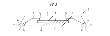
図1は、本発明の一実施の形態である半導体装置1の平面(上面)透視図であり、図2はその断面図、図3はその底面図(裏面図)である。図1は、封止樹脂部2を透視したときの平面(上面)図に対応する。また、図1のA−A線の断面が図2にほぼ対応する。
1 is a plan (top) perspective view of a
本実施の形態の半導体装置1は、樹脂封止形で、面実装形の半導体パッケージであり、例えばQFN(Quad Flat Non leaded package)形態の半導体装置である。
The
図1〜図3示される本実施の形態の半導体装置1は、封止樹脂部(封止部)2と、封止樹脂部2によって封止された半導体チップ(半導体素子)3と、導電体によって形成された複数のリード(リード部)4と、封止樹脂部2によって封止されかつ複数のリード4と半導体チップ3の表面の複数の電極(ボンディングパッド、パッド電極)3aとを電気的に接続する複数のボンディングワイヤ6と、半導体チップ3が搭載されたチップ搭載部であるタブ(ダイパッド部、チップ搭載部)7と、タブ7に接続された複数の吊りリード(導体部)8とを備えている。
1 to 3 includes a sealing resin part (sealing part) 2, a semiconductor chip (semiconductor element) 3 sealed with the sealing
封止樹脂部2は、例えば熱硬化性樹脂材料などの樹脂材料などからなり、フィラーなどを含むこともできる。例えば、フィラーを含むエポキシ樹脂などを用いて封止樹脂部2を形成することができる。封止樹脂部2により、半導体チップ3、リード4、ボンディングワイヤ6、タブ7および吊りリード8が封止され、保護される。封止樹脂部2の裏面(実装面)2aが、半導体装置1の実装面である。
The sealing
半導体チップ3は、例えば、単結晶シリコンなどからなる半導体基板(半導体ウエハ)に種々の半導体素子または半導体集積回路を形成した後、必要に応じて半導体基板の裏面研削を行ってから、ダイシングなどにより半導体基板を各半導体チップ3に分離したものである。半導体チップ3は、その表面(半導体素子形成側の主面)が上方を向くようにタブ7上に搭載され、半導体チップ3の裏面(半導体素子形成側の面とは逆側の主面)が導電体からなるタブ7に、例えば銀ペーストまたは絶縁ペーストなどの接合材(図示せず)を介して接着(接合)されている。
For example, the
半導体チップ3の表面には、複数の電極3aが形成されている。電極3aは、半導体チップ3に形成された半導体素子または半導体集積回路に電気的に接続されている。半導体チップ3の表面の各電極3aは、各リード4の上面4aに、例えば金(Au)線などの金属細線などからなるボンディングワイヤ6を介して電気的に接続されている。
A plurality of
リード4はタブ7の周囲に、その一端がタブ7に対向するように配置されている。リード4は、封止樹脂部2に埋め込まれたインナリードと、封止樹脂部2の裏面2aに露出するアウタリードとの両者の機能を兼ねている。すなわち、封止樹脂部2によって封止され、リード4のボンディング部として機能し得るリード4の上面4aに、ボンディングワイヤ6が接続(接合)され、封止樹脂部2の裏面2aに、外部接続用端子部として機能し得るリード4の下面の露出部である下部露出面4bが露出している。リード4の上面4aには、ボンディングワイヤ6の接続を容易にするためにめっき層(例えば銀めっき層)を形成することもできる。リード4の下部露出面4bは、例えば略長方形状を有している。
The
リード4のタブ7に対向する側の端部とは逆側の端部として、リード4の切断面(側面、端面)4cが封止樹脂部2の切断面(側面)2bで露出している。リード4の切断面4cおよび封止樹脂部2の切断面2bは、半導体装置を製造する際の切断工程により生じた側面(端面)である。
The cut surface (side surface, end surface) 4c of the
リード4と半導体チップ3との間は封止樹脂部2を構成する材料で満たされており、リード4と半導体チップ3とが接触しないようになっている。また、隣り合うリード4間は封止樹脂部2を構成する材料により満たされており、互いに接触しないようになっている。
The space between the
封止樹脂部2の裏面2aに対応する半導体装置1の裏面(底面)が、半導体装置1の実装面となり、各リード4の下部露出面4bが封止樹脂部2の裏面2a(すなわち半導体装置1の裏面)で露出して半導体装置1の外部端子(外部接続用端子)を構成する。また、封止樹脂部2の裏面2aで露出するリード4の下部露出面4b上にはめっき層(例えば半田めっき層)が形成されているが、理解を簡単にするために、めっき層の図示を省略している。リード4の下部露出面4b上にめっき層が形成されていることで、半導体装置1を基板(外部基板、マザーボード)に実装する際に、基板上の端子または導体パターンと半導体装置1の端子(リード4の下部露出面4b)との間の電気的接続の信頼性を向上することができる。
The back surface (bottom surface) of the
タブ7には、複数(ここでは4本)の吊りリード(導体部)8が接続されている。各吊りリード8は、導電体材料からなり、一端がタブ7に接続され、タブ7の外方に向かって延在している。吊りリード8は、半導体装置1の製造に用いられたリードフレーム(のフレーム枠)にタブ7を保持または支持するために設けられ、封止樹脂部2の形成後にリードフレームから切断され、吊りリード8の切断により生じた側面(すなわちタブ7に接続された側の端部とは逆側の端部)である切断面8cが封止樹脂部2の切断面(側面)2bで露出している。吊りリード8の下面の一部は封止樹脂部2の裏面2aで露出しており、ここでは吊りリード8の切断面8c近傍領域の下面である下部露出面8bが、封止樹脂部2の裏面2aで露出している。吊りリード8には屈曲部が設けられており、吊りリード8のうち下部露出面8bよりもタブ7側の部分は上方に持ち上げられて、タブ7とともに封止樹脂部2内に封止されている。リード4、タブ7および吊りリード8は、いずれも導電体材料からなり、例えば半導体装置の製造の際にリードフレームに用いられた共通の導電体材料からなる。
A plurality of (here, four) suspension leads (conductor portions) 8 are connected to the
上記のように、半導体チップ3の複数の電極3aと複数のリード4とが複数のボンディングワイヤ6を介して電気的に接続されている。半導体チップ3の各電極3aにボンディングワイヤ6の一端が接続され、ボンディングワイヤ6の他端が各リード4の上面4aに接続される。本実施の形態の半導体装置1では、電気特性改善や向上のために、半導体チップ3の複数の電極3aにそれぞれ接続した複数のボンディングワイヤ6を同じ(一つの)リード4に対して接続する多重ボンディング(いわゆるダブルボンディングやトリプルボンディングなど)が行われている。例えば、図1では、それぞれ半導体チップ3の電極3aに一端が接続された2本のボンディングワイヤ6の他端が、同じ(一つの)リード4dに接続(いわゆるダブルボンディング)され、それぞれ半導体チップ3の電極3aに一端が接続された2本のボンディングワイヤ6の他端が、同じ(一つの)リード4eに接続(いわゆるダブルボンディング)され、それぞれ半導体チップ3の電極3aに一端が接続された3本のボンディングワイヤ6の他端が、同じ(一つの)リード4fに接続(いわゆるトリプルボンディング)されている。図1では、複数のリード4のうち、リード4dには2本、リード4eには2本、リード4fには3本、他のリード4には1本のボンディングワイヤ6がそれぞれ接続されているが、一つのリード4に接続されるボンディングワイヤ6の数はこれに限定されるものではなく、例えば4本以上のボンディングワイヤ6を同じ(一つの)リード4に対して接続することもできる。
As described above, the plurality of
本実施の形態では、リード4d,4e,4fのように同じ(一つの)リード4に複数のボンディングワイヤ6を接続する場合、後述するように、そのリード4の同じ位置にワイヤボンディングを行い、そのリード4(リード4d,4e,4f)に接続する各ボンディングワイヤ6の接合部が重なる(積み重なる)ようにしている。このため、本実施の形態の半導体装置1では、リード4d,4e,4fのそれぞれにおいて、複数のボンディングワイヤ6の接合部が重なっている。
In the present embodiment, when a plurality of
次に、本実施の形態の半導体装置の製造工程について説明する。図4〜図7は、本実施の形態の半導体装置の製造工程を示す断面図(要部断面図)である。図4〜図7は、図2に対応する断面が示されている。また、図4〜図7には、リードフレーム11の一つの半導体パッケージに対応する領域(そこから一つの半導体装置1が製造される領域)が示されている。
Next, the manufacturing process of the semiconductor device of this embodiment will be described. 4 to 7 are cross-sectional views (main-part cross-sectional views) showing the manufacturing process of the semiconductor device of the present embodiment. 4 to 7 show cross sections corresponding to FIG. 4 to 7 show a region corresponding to one semiconductor package of the lead frame 11 (a region from which one
まず、図4に示されるように、半導体装置1の製造に用いられるリードフレーム11を準備する。リードフレーム11は、例えば、銅または銅合金、あるいは42−アロイなどの導電体材料からなる。リードフレーム11は、半導体チップ3を搭載するためのタブ7と、その一端がタブ7と離間して対向するように配置され他端がリードフレーム11のフレーム枠(図示せず)と接続するリード4とを有している。また、図4の断面には示されていないけれども、タブ7の四隅に吊りリード8の一端が接続し吊りリード8の他端がフレーム枠に接続してタブ7がリードフレーム11のフレーム枠に保持または支持されている。
First, as shown in FIG. 4, a
次に、図5に示されるように、リードフレーム11のタブ7上に半導体チップ3を銀ペーストまたは絶縁ペーストなどの接合材(図示せず)を介して接着(接合)する。
Next, as shown in FIG. 5, the
次に、図6に示されるように、ワイヤボンディング工程を行って、半導体チップ3の複数の電極3aとリードフレーム11の複数のリード4の上面4aとを複数のボンディングワイヤ6を介してそれぞれ電気的に接続する。この際、ボンディングワイヤ6の一端を半導体チップ3の電極3aに接続(ファーストボンディング)してから、ボンディングワイヤ6の他端をリード4に接続(セカンドボンディング)する。
Next, as shown in FIG. 6, a wire bonding step is performed to electrically connect the plurality of
次に、図7に示されるように、モールド工程(例えばトランスファモールド工程)を行って、半導体チップ3、ボンディングワイヤ6およびタブ7を封止樹脂部2によって封止する。封止樹脂部2は、例えば熱硬化性樹脂材料などの樹脂材料などからなり、フィラーなどを含むこともできる。例えば、フィラーを含むエポキシ樹脂などを用いて封止樹脂部2を形成することができる。また、封止樹脂工程では、封止樹脂部2の裏面2aからリード4の下面である下部露出面4bが露出するように、封止樹脂部2を形成する。
Next, as shown in FIG. 7, a molding process (for example, a transfer molding process) is performed to seal the
次に、必要に応じてリードフレーム11の封止樹脂部2から露出する部分(導電体からなる部分)上にめっき層(図示せず)を形成した後、リードフレーム11が所定の位置で切断されて、図1〜図3に示されるような個片に分割された半導体装置1が得られる(製造される)。
Next, after forming a plating layer (not shown) on a portion exposed from the sealing
次に、本実施の形態の半導体装置の製造工程におけるワイヤボンディング工程について説明する。 Next, the wire bonding process in the manufacturing process of the semiconductor device of this embodiment will be described.
図8〜図11は、ワイヤボンディング工程(半導体チップ3の電極3aとリード4との間をボンディングワイヤ6で接続する工程)の一例を示す説明図である。
8 to 11 are explanatory views showing an example of a wire bonding step (step of connecting the
まず、図8に示されるように、放電などによって先端に金球21aを形成した金線21(ボンディングワイヤ6形成用の金線21)がワイヤボンディング装置のキャピラリ(ボンディングツール)22に保持され、半導体チップ3の電極3a上に待機している。金線21の直径は例えば25〜30μm程度である。それから、図9に示されるように、待機していた金線21をファーストボンディングである半導体チップ3の電極3a上に適切な荷重をもって接触させ、金球21aが電極3aに接触した後、キャピラリ22を超音波振動させ、このときの荷重や印加された超音波によるエネルギーで金球21aと電極3aとを接合(接続)させる。
First, as shown in FIG. 8, a gold wire 21 (
次に、図10に示されるように、キャピラリ22が適切な軌跡を描きながら移動して、リード4の上面に移動する。この軌跡によって、ボンディングワイヤの適切なループ形状が得られる。そして、リード4の上面4aに対してキャピラリ22に保持された金線21が適切な荷重をもって押し付けられ、キャピラリ22が超音波振動する。このときの荷重や印加された超音波によるエネルギーで金線21とリード4の上面4aとを接合(接続)させる。
Next, as shown in FIG. 10, the capillary 22 moves while drawing an appropriate locus, and moves to the upper surface of the
その後、図11に示されるように、キャピラリ22が上昇する過程でワイヤクランパ23で金線21を保持し、金線21をセカンドボンディング点(接合部)から切断する。このようにして、半導体チップ3の電極3aとリード4の上面4aとの間を金線21(金球21aを含む金線21)からなるボンディングワイヤ6で電気的に接続することができる。
Thereafter, as shown in FIG. 11, the
図12は、上記のようにしてリード4の上面に金線21(ボンディングワイヤ6)を接合した状態を示す説明図(斜視図)であり、リード4の先端部(タブ7に対向する側の端部)近傍領域が示されている。なお、図12に示されるリード4の先端部近傍の上面4aには、金線21(ボンディングワイヤ6)の接続を容易にするためにめっき層(例えば銀めっき層)が形成されている。
FIG. 12 is an explanatory view (perspective view) showing a state in which the gold wire 21 (bonding wire 6) is bonded to the upper surface of the
セカンドボンディングにおいては、図10に示されるように、金線21を接続する面、ここではリード4の上面4aにキャピラリ22を押し付けるので、図12に示されるように、リード4の上面4aにはツールマーク(ボンディングツールの痕、ツール痕、キャピラリ痕)31が残る。ツールマーク31は、ワイヤボンディングの際にボンディングツールとしてのキャピラリ22が押し付けられることによってリード4の上面(平坦面)4aに生じた凹凸または窪みである。リード4の上面4aに対する金線21(ボンディングワイヤ6)の接合部(圧着部)32は、ツールマーク31内に位置することになる。ツールマーク31の平面形状または平面寸法(外形寸法)は、リード4に接触するキャピラリ22の先端部形状または寸法にほぼ対応し、例えば直径100μm程度の略円形などである。
In the second bonding, as shown in FIG. 10, the capillary 22 is pressed against the surface to which the
このようにして、半導体チップ3の複数の電極3aとリードフレーム11の複数のリード4の上面4aとを複数のボンディングワイヤ6を介してそれぞれ電気的に接続することができる。
In this way, the plurality of
本実施の形態においては、図1に示されるように、電気特性改善や向上のために、半導体チップ3の複数の電極3aにそれぞれ接続した複数のボンディングワイヤ6を同じ(一つの)リード4に対して接続する多重ボンディングが行われている。しかしながら、本発明者の検討によれば、同じ(一つの)リード4に対して複数のボンディングワイヤ6を接続した場合、次のような問題点が生じる可能性があることが分かった。
In the present embodiment, as shown in FIG. 1, a plurality of
図13は、同じ(一つの)リードに対して複数のボンディングワイヤを接続した場合に生じ得る問題点(第1の問題点)の説明図(斜視図)であり、第1の比較例のワイヤボンディング(リードに対するボンディングワイヤの接続工程)の説明図に対応する。 FIG. 13 is an explanatory view (perspective view) of a problem (first problem) that may occur when a plurality of bonding wires are connected to the same (one) lead, and the wire of the first comparative example It corresponds to an explanatory view of bonding (bonding wire connecting step to lead).
図13では、一つのリード34(本実施の形態のリード4に対応)に対して複数のボンディングワイヤ、ここでは2本のボンディングワイヤ6a,6bを接続している。ボンディングワイヤ6a,6bは、それぞれ、図8〜図11のようにして形成される。図13では、リード34の上面34a(上面4aに対応)におけるボンディングワイヤ6a,6bの接合部(圧着部、ボンディング部)32a,32bを平面的に並べて、各ボンディングワイヤ6a,6bの接続の際のツールマーク31a,31bが重ならないようにしている。すなわち、リード34の上面34aにボンディングワイヤ6aを接続した後に、同じリード34の上面34aにボンディングワイヤ6bを接続しているが、ボンディングワイヤ6aの接続の際に生じたツールマーク31aに、ボンディングワイヤ6bの接続の際に生じるツールマーク31bが重ならないようにしている。
In FIG. 13, a plurality of bonding wires, here two
ツールマーク31a,31b同士が重ならず、凹凸面(窪み部分)であるツールマーク31a外のリード34の平坦な領域にボンディングワイヤ6bを接続(接合)できるので、ボンディングワイヤ6a,6bのリード34の上面34aへの接続の信頼性(接続強度)を高めることができる。
Since the tool marks 31a and 31b do not overlap with each other and the
しかしながら、図13の場合は、ツールマーク31a,31bが重ならないようにボンディングワイヤ6a,6bをリード34に接続するので、ボンディングワイヤ6aの接合部32aとボンディングワイヤ6bの接合部32bとの間が比較的大きな間隔を空けて離れることになり、リード34の上面34aにおいてワイヤボンディングに要する領域が大きくなってしまう。このため、図13では、リード34の幅を広くし、ボンディングワイヤ6a,6bを接続するための平坦領域(上面34a)を大きくする必要がある。このように、リード34の面積(または幅)を比較的大きくする必要があるので、半導体装置の小型化が困難になるという第1の問題点が生じる。
However, in the case of FIG. 13, since the
このため、リードの幅を比較的小さくして半導体装置の小型化を実現するために、一つのリードに対して複数のボンディングワイヤを接続する際に、ツールマークが部分的に重なるように、ワイヤボンディングを行うことが考えられる。図14は、同じ(一つの)リードに対して複数のボンディングワイヤを接続した場合に生じ得る他の問題点(第2の問題点)の説明図(斜視図)であり、第2の比較例のワイヤボンディング(リードに対するボンディングワイヤの接続工程)の説明図に対応する。 For this reason, in order to achieve a reduction in the size of the semiconductor device by relatively reducing the width of the lead, when connecting a plurality of bonding wires to one lead, the wire is arranged so that the tool mark partially overlaps. It is conceivable to perform bonding. FIG. 14 is an explanatory diagram (perspective view) of another problem (second problem) that may occur when a plurality of bonding wires are connected to the same (one) lead, and is a second comparative example. This corresponds to an explanatory diagram of wire bonding (bonding wire connecting step to lead).
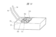
図14では、一つのリード35(本実施の形態のリード4に対応)に対して複数のボンディングワイヤ、ここでは2本のボンディングワイヤ6c,6dを接続している。ボンディングワイヤ6c,6dは、それぞれ、図8〜図11のようにして形成される。図14では、リード35の上面35a(上面4aに対応)におけるボンディングワイヤ6c,6dの接合部(圧着部、ボンディング部)32c,32dを近づけて各ボンディングワイヤ6c,6dのツールマーク31c,31dが部分的に重なるようにしている。すなわち、リード35の上面35aにボンディングワイヤ6cを接続した後に、同じリード35の上面35aにボンディングワイヤ6dを接続しているが、ボンディングワイヤ6cの接続の際に生じたツールマーク31cに、ボンディングワイヤ6dの接続の際に生じるツールマーク31dの一部が重なるようにしている。
In FIG. 14, a plurality of bonding wires, here two
図14の場合は、ツールマーク31c,31d同士が部分的に重なるので、ボンディングワイヤ6cの接合部32cとボンディングワイヤ6dの接合部32dとの間が図13の場合よりも小さな間隔を空けて離れることになる。このため、図14の場合は、図13の場合に比べて、リード35の上面35aにおいてワイヤボンディングに要する領域を小さくすることができ、リード35の幅をリード34よりも小さくすることができ、半導体装置の小型化に有利である。しかしながら、図14の場合は、ボンディングワイヤ6cの接続後に行うボンディングワイヤ6dの接続の際に、凹凸面(または窪み)であるツールマーク31cにキャピラリ22が部分的に重なり(ずれた状態で重なり)、更にツールマーク31cの端部の段差にボンディングワイヤ6dの接合部(圧着部)32dが重なってしまう。このため、ボンディングワイヤ6dの接続の接続強度が低下し、ボンディングワイヤ6dの接続の信頼性が低下する可能性がある。
In the case of FIG. 14, since the tool marks 31c and 31d partially overlap each other, the
図15〜図17は、本実施の形態におけるワイヤボンディング(リード4に対するボンディングワイヤ6の接続工程)の説明図である。図15は、ボンディングワイヤ6のうちの2本のボンディングワイヤ6e,6fを同じリード4に順に接続した後の状態を示す斜視図に対応し、図16は、図15の拡大図に対応する。図17は、リード4にボンディングワイヤ6eを接続した後、そのリード4に次のボンディングワイヤ6fを接続する工程中の図10の状態の概念的な側面断面図に対応する。このため、図17では、ボンディングワイヤ6fはまだ切断されていない。また、図15〜図17に示されるリード4は、例えば図1のリード4dまたはリード4eに対応する。
15 to 17 are explanatory diagrams of wire bonding (a step of connecting the
本実施の形態では、図15〜図17に示されるように、同じ(一つの)リード4に対して複数のボンディングワイヤ6(図15〜図17の例では2本のボンディングワイヤ6e,6f)を接続する際に、そのリード4の上面4aにおける複数のボンディングワイヤ6(ボンディングワイヤ6e,6f)の接合部(図15〜図17の例では接合部32e,32f)がほぼ重なる(一致する)ようにワイヤボンディング(ボンディングワイヤ6a,6bの接続)を行っている。すなわち、同じ(一つの)リード4に対して複数のボンディングワイヤ6(ボンディングワイヤ6a,6b)を接続する際に、そのリード4の上面4aに生じるツールマーク(ツールマーク31e,31f)が平面的にほぼ重なる(一致する)ようにワイヤボンディング(ボンディングワイヤ6a,6bの接続)を行っている。
In the present embodiment, as shown in FIGS. 15 to 17, a plurality of bonding wires 6 (two
図15〜図17では、リード4の上面4aにボンディングワイヤ6eを接続した後に、同じリード4の上面4aにボンディングワイヤ6fを接続しているが、ボンディングワイヤ6eの接続の際に生じたツールマーク(ボンディングツールの痕、ツール痕、キャピラリ痕)31eに、ボンディングワイヤ6fの接続の際に生じるツールマーク31fが平面的にほぼ重なる(一致する)ようにしている。この際、上記図14に示されるように、ツールマーク同士の重なり領域が少ないと、ボンディングワイヤの接続の信頼性が低下する可能性がある。それに対して、本実施の形態では、図15〜図17に示されるように、ツールマーク31e,31f同士の重なり領域を相対的に大きくしてツールマーク31e,31fが実質的に重なる(一致する)ようにしており、リード4の上面4aに対するボンディングワイヤ6eの接合部(圧着部、ボンディング部)32eとボンディングワイヤ6fの接合部(圧着部、ボンディング部)32fとが多段に(上下に)積み重なるようにしている。このため、ボンディングワイヤ6eの接続後に行うボンディングワイヤ6fの接続の際に、リード4の上面4aに接触させた(押し付けた)キャピラリ22が凹凸面(窪み)であるツールマーク32eに実質的に重なってそれらの凹凸形状がほぼ一致する。しかも、ツールマーク31eの端部の段差にボンディングワイヤ6fの接合部(圧着部)32fが重ならない。このため、的確かつスムースにボンディングワイヤ6fをリード4に接合することができ、ボンディングワイヤ6fの接続の接続強度を向上し、ボンディングワイヤ6fの接続の信頼性を向上することができる。これにより、ボンディングワイヤ6e,6fを含むボンディングワイヤ6の接続の信頼性を向上でき、半導体装置1の信頼性を向上することができる。また、半導体装置の製造歩留りを向上することもできる。
15 to 17, after the
また、本実施の形態では、図15および図16に示されるように、リード4の上面4aには、ボンディングワイヤ6e,6fの接続を容易にするためにめっき層(例えば銀めっき層)36が形成されており、ボンディングワイヤ6e,6fは、このリード4の上面4aのめっき層36に接続されている。これにより、ボンディングワイヤ6e,6fを含むボンディングワイヤ6の接続の信頼性をより向上することができる。
In this embodiment, as shown in FIGS. 15 and 16, a plating layer (for example, a silver plating layer) 36 is provided on the
また、本実施の形態では、図13や図14の場合に比べて、リード4の上面4aにおいてワイヤボンディングに要する領域(面積)を小さくすることができる。このため、リード4の幅または平面寸法を比較的小さくすることができ、半導体装置1を小型化することができる。また、インナリード部(リード4)の平坦領域の省スペース化が可能になるので、例えばQFNパッケージのようにインナリード部(リード4)の上面の平坦領域が小さい半導体装置においても、多重ボンディングが可能になる。
Further, in the present embodiment, the region (area) required for wire bonding can be reduced on the
また、本実施の形態では、上記のように、同じリード4に対して複数のボンディングワイヤ6e,6fを接続する際に、各ワイヤボンディングで生じるツールマーク31e,31fをほぼ一致させるが、若干ずれた場合でも、そのずれが小さければ上記のような効果を得ることは可能である。例えば、各ボンディングワイヤ6e,6fの接合部32e,32fが部分的に重なれば、有効である。各ツールマーク31e,31fの中心位置のずれ(平面的なずれ)は、ボンディングワイヤ6の直径(例えば25〜30μm程度)以下であることが好ましく、ワイヤボンディング装置によるワイヤボンディング位置の制御の精度の範囲内(例えば10μm程度以下)であればより好ましく、ツールマーク31e,31fが実質的に一致すれば更に好ましい。これにより、上記のような効果(ボンディングワイヤの接続の信頼性向上や半導体装置の小型化など)を的確に得ることが可能になる。
Further, in the present embodiment, as described above, when a plurality of
また、図15〜図17では、それぞれ半導体チップ3の電極3aに一端が接続された2本のボンディングワイヤ6e,6fの他端が、同じ(一つの)リード4に接続(いわゆるダブルボンディング)されているが、一つのリード4に接続されるボンディングワイヤ6の数はこれに限定されるものではなく、必要に応じて任意の数のボンディングワイヤ6を一つのリード4に対して接続することができる。例えば3本以上のボンディングワイヤ6を同じ(一つの)リード4に接続する場合でも、それらのボンディングワイヤ6のツールマークが互いにほぼ重なる(一致する)ようにし、各ボンディングワイヤ6の接合部が積み重なるように、各ボンディングワイヤ6のリード4への接続(ワイヤボンディング)を行う。
15 to 17, the other ends of the two
本実施の形態では、半導体チップ3の複数の電極3aと複数のリード4とを複数のボンディングワイヤ6を介して電気的に接続するが、あるリード4に対して複数のボンディングワイヤ6を接続する際に、そのリードに生じ得るツールマークが平面的に重なる(一致する)ようにする。ツールマークが重なるようにしボンディングワイヤ6の接合部(圧着部)を積み重ねていくので、ワイヤボンディングに要するリード4の上面の平坦部面積は、そのリードに接続されるボンディングワイヤ6の数に影響されない。このため、リード4の平坦部面積が狭い場合であっても、多重ボンディングが可能になる。
In the present embodiment, the plurality of
また、本実施の形態は、比較的幅が狭く長さが短いリードを用いるQFNパッケージ形態の半導体装置に適用すれば特に有効であるが、QFP(Quad Flat Package、Quad Flat gull wing leaded Package)形態の半導体装置などに適用しても効果がある。 The present embodiment is particularly effective when applied to a semiconductor device of a QFN package type using a lead having a relatively small width and a short length, but a QFP (Quad Flat Package, Quad Flat Gull Wing Leaded Package) type. The present invention is also effective when applied to such semiconductor devices.
(実施の形態2)
図18は、本発明の他の実施の形態におけるワイヤボンディング(リード4に対するボンディングワイヤ6の接続工程)の説明図であり、上記実施の形態1における図17に対応する。
(Embodiment 2)
FIG. 18 is an explanatory diagram of wire bonding (a step of connecting the
本実施の形態は、半導体装置の構造および半導体装置の製造工程のうち、ワイヤボンディング(リード4に対するボンディングワイヤ6の接続工程および接続構造)以外については上記実施の形態1と同様であるので、ここではその説明を省略する。
The present embodiment is the same as the first embodiment except for the wire bonding (the bonding process of the
本実施の形態においても、上記実施の形態1と同様に、半導体チップ3の複数の電極3aと複数のリード4とを複数のボンディングワイヤ6を介して電気的に接続するが、あるリード4に対して複数のボンディングワイヤ6を接続する。図18の例では、同じ(一つの)リード4に対して2本のボンディングワイヤ6e,6fを接続する。本実施の形態では、ボンディングワイヤ6eの接合部32eとボンディングワイヤ6fの接合部32f間に金(Au)ボール(金を含む部材)41を介在させる。
Also in the present embodiment, as in the first embodiment, the plurality of
本実施の形態では、上記実施の形態1における図8〜図11のようにしてリード4にボンディングワイヤ6eを接続(接合)した後、リード4の上面4aにおけるボンディングワイヤ6eの接合部32e上に金ボール(圧着金ボール)41を例えば圧着などにより形成する。金ボール41は、ボンディングワイヤ6(ボンディングワイヤ6e,6f)と同じ材料(ここでは金(Au))からなることが好ましい。
In the present embodiment, the
金ボール41は、例えば、放電などによって先端に金球を形成した金線をワイヤボンディング装置のキャピラリ22に保持し、ボンディングワイヤ6eが既に接続されたリード4上に金ボールを適切な荷重をもって接触させた後、キャピラリ22を超音波振動させ、このときの荷重や印加された超音波によるエネルギーでボンディングワイヤ6eが接続されたリード4に金球を接着(接合)させ、金線を引きちぎってボンディングワイヤ6aが接続されたリード4に残存する金球からなる金ボール41を形成することができる。
For example, the
リード4の上面4aにおけるボンディングワイヤ6eの接合部32e上に金ボール41を形成した後、このリード4上にボンディングワイヤ6fを図8〜図11のようにして接続する。この際、リード4の上面4aのボンディングワイヤ6eの接合部32e上に金ボール41を介してボンディングワイヤ6fを接合する。また、上記実施の形態1と同様に、リード4の上面4aに生じるツールマークが平面的に重なる(一致する)ようにワイヤボンディングを行うことで、リード4の上面4aのボンディングワイヤ6e,6fの接合部(圧着部、ボンディング部)32e,32fが重なるようにしている。このため、ボンディングワイヤ6eの接合部32eとボンディングワイヤ6fの接合部32fとの間には、ボンディングワイヤ6fの接合時に押しつぶされた金ボール41が介在し、ボンディングワイヤ6eの接合部32e、押しつぶされた金ボール41およびボンディングワイヤ6fの接合部32fが上下方向に積み重なることになる。
After the
本実施の形態では、このように、リード4にボンディングワイヤ6eを接続した後、金ボール41を形成し、この金ボール41を介してボンディングワイヤ6fをリード4の上面4a(またはボンディングワイヤ6fの接合部32f)上に接合する。ボンディングワイヤ6eの接合部32eとボンディングワイヤ6fの接合部32fとの間の金ボール41は、緩衝材(クッション)として機能することができる。このため、ボンディングワイヤ6fの接続時に、その下に位置するボンディングワイヤ6e(の接合部32e)とリード4との間の接合がダメージを受けるのを抑制または防止することができる。これにより、ボンディングワイヤ6eの接続強度をより向上することができる。また、金ボール41を設けたことにより、ボンディングワイヤ6fもリード4に、より確実に接続することができ、ボンディングワイヤ6fの接続強度をより向上することができる。従って、ボンディングワイヤ6e,6fの接続強度や接続の信頼性をより向上することができる。これにより、半導体装置の信頼性をより向上し、製造歩留りをより向上することが可能になる。
In the present embodiment, after the
また、ボンディングワイヤ6fを金ボール41を介して接続したことにより、図18に示されるように、ボンディングワイヤ6e,6f間の上下方向(リード4の上面4aに垂直な方向)の間隔(距離)を金ボール41がない場合に比べて相対的に大きくすることができる。このため、ボンディングワイヤ6eとボンディングワイヤ6fとが、金ボール41を介した接続部以外の途中の領域で互いに接触することを防止することができる。ボンディングワイヤ6e,6f間の接触を防止することができるので、半導体装置の信頼性をより向上することができる。
Further, since the
また、本実施の形態においても、上記実施の形態1と同様に、ツールマーク同士がほぼ重なるように複数のボンディングワイヤ6e,6fを同じ(一つの)リード4に接続することができるので、リード4の上面4aにおいてワイヤボンディングに要する領域(面積)を小さくすることができる。このため、リード4の幅または平面寸法を比較的小さくすることができ、半導体装置1を小型化することができる。また、インナリード部(リード4)の平坦領域の省スペース化が可能になるので、例えばQFNパッケージのようにインナリード部(リード4)の上面の平坦領域が小さい半導体装置においても、多重ボンディングが可能になる。
Also in the present embodiment, as in the first embodiment, since a plurality of
また、本実施の形態は、比較的幅が狭く長さが短いリードを用いるQFNパッケージ形態の半導体装置に適用すれば特に有効であるが、QFP形態の半導体装置などに適用しても効果がある。 This embodiment is particularly effective when applied to a QFN package type semiconductor device using a lead having a relatively small width and a short length, but is also effective when applied to a QFP type semiconductor device or the like. .
以上、本発明者によってなされた発明をその実施の形態に基づき具体的に説明したが、本発明は前記実施の形態に限定されるものではなく、その要旨を逸脱しない範囲で種々変更可能であることは言うまでもない。 As mentioned above, the invention made by the present inventor has been specifically described based on the embodiment. However, the invention is not limited to the embodiment, and various modifications can be made without departing from the scope of the invention. Needless to say.
前記実施の形態では、QFN(Quad Flat Non leaded package)形態の半導体装置に適用した場合について説明したが、本発明は、これに限定されるものではなく、QFP(Quad Flat Package、Quad Flat gull wing leaded Package)など、半導体チップの複数の電極と複数のリード部とを複数のワイヤを介して電気的に接続した種々の半導体パッケージ形態の半導体装置に適用することができる。 In the above-described embodiment, the case where the present invention is applied to a semiconductor device of QFN (Quad Flat Non leaded package) type has been described, but the present invention is not limited to this, and QFP (Quad Flat Package, Quad Flat gull wing) The present invention can be applied to various semiconductor package semiconductor devices in which a plurality of electrodes of a semiconductor chip and a plurality of lead portions are electrically connected via a plurality of wires, such as a leaded package.
本発明は、半導体パッケージ形態の半導体装置に適用して有効である。 The present invention is effective when applied to a semiconductor device in the form of a semiconductor package.
1 半導体装置
2 封止樹脂部
2a 裏面
2b 切断面
3 半導体チップ
3a 電極
4 リード
4a 上面
4b 下部露出面
4c 切断面
4d リード
4e リード
4f リード
6 ボンディングワイヤ
6a ボンディングワイヤ
6b ボンディングワイヤ
6c ボンディングワイヤ
6d ボンディングワイヤ
6e ボンディングワイヤ
6f ボンディングワイヤ
7 タブ
8 吊りリード
8b 下部露出面
8c 切断面
11 リードフレーム
12 モールドライン
13 フレーム枠
21a 金球
21 金線
21b 接合部
22 キャピラリ
23 ワイヤクランパ
31 ツールマーク
31a ツールマーク
31b ツールマーク
31c ツールマーク
31d ツールマーク
31e ツールマーク
31f ツールマーク
32 接合部
32a 接合部
32b 接合部
32c 接合部
32d 接合部
32e 接合部
32f 接合部
34 リード
34a 上面
35 リード
35a 上面
36 めっき層
41 金ボール
DESCRIPTION OF
Claims (5)
導電体により形成された複数のリード部と、
前記複数のリード部と前記半導体チップの前記複数の電極とを電気的に接続する複数のワイヤと、
前記半導体チップ、前記複数のワイヤおよび前記複数のリード部を封止する封止樹脂部と、
を具備し、
前記複数のリード部のうちの第1リード部に前記複数のワイヤのうちの複数の第1ワイヤが接続され、前記第1リード部における前記各第1ワイヤの接合部が重なっていることを特徴とする半導体装置。 A semiconductor chip having a plurality of electrodes;
A plurality of lead portions formed of a conductor;
A plurality of wires that electrically connect the plurality of lead portions and the plurality of electrodes of the semiconductor chip;
A sealing resin portion for sealing the semiconductor chip, the plurality of wires, and the plurality of lead portions;
Comprising
A plurality of first wires of the plurality of wires are connected to a first lead portion of the plurality of lead portions, and a joint portion of the first wires in the first lead portion overlaps. A semiconductor device.
(b)導電体からなる複数のリード部と前記半導体チップの前記複数の電極とを複数のワイヤを介して電気的に接続し、前記複数のリード部のうちの第1リード部に前記複数のワイヤのうちの複数の第1ワイヤを接続する工程、
を有し、
前記(b)工程では、前記第1リード部における前記各第1ワイヤの接合部が重なるように、前記複数の第1ワイヤを前記第1リード部に接続することを特徴とする半導体装置の製造方法。 (A) preparing a semiconductor chip having a plurality of electrodes;
(B) A plurality of lead portions made of a conductor and the plurality of electrodes of the semiconductor chip are electrically connected via a plurality of wires, and the plurality of lead portions are connected to a first lead portion of the plurality of lead portions. Connecting a plurality of first wires of the wires;
Have
In the step (b), the plurality of first wires are connected to the first lead portion so that the joint portions of the first wires in the first lead portion overlap each other. Method.
(b)導電体からなる複数のリード部と前記半導体チップの前記複数の電極とを複数のワイヤを介して電気的に接続し、前記複数のリード部のうちの第1リード部に前記複数のワイヤのうちの複数の第1ワイヤを接続する工程、
を有し、
前記(b)工程では、前記各第1ワイヤを前記第1リード部に接続する際のツールマークが重なるように、前記複数の第1ワイヤを前記第1リード部に接続することを特徴とする半導体装置の製造方法。 (A) preparing a semiconductor chip having a plurality of electrodes;
(B) A plurality of lead portions made of a conductor and the plurality of electrodes of the semiconductor chip are electrically connected via a plurality of wires, and the plurality of lead portions are connected to a first lead portion of the plurality of lead portions. Connecting a plurality of first wires of the wires;
Have
In the step (b), the plurality of first wires are connected to the first lead portion so that tool marks for connecting the first wires to the first lead portion overlap each other. A method for manufacturing a semiconductor device.
(b)導電体からなる複数のリード部と前記半導体チップの前記複数の電極とを複数のワイヤを介して電気的に接続し、前記複数のリード部のうちの第1リード部に前記複数のワイヤのうちの複数の第1ワイヤを接続する工程、
を有し、
前記(b)工程では、前記第1リード部における前記各第1ワイヤの接合部が間に金を含む部材を介在して重なるように、前記複数の第1ワイヤを前記第1リード部に接続することを特徴とする半導体装置の製造方法。 (A) preparing a semiconductor chip having a plurality of electrodes;
(B) A plurality of lead portions made of a conductor and the plurality of electrodes of the semiconductor chip are electrically connected via a plurality of wires, and the plurality of lead portions are connected to a first lead portion of the plurality of lead portions. Connecting a plurality of first wires of the wires;
Have
In the step (b), the plurality of first wires are connected to the first lead portion so that the joint portions of the first wires in the first lead portion overlap with a member including gold interposed therebetween. A method of manufacturing a semiconductor device.
(b)導電体からなる複数のリード部と前記半導体チップの前記複数の電極とを複数のワイヤを介して電気的に接続し、前記複数のリード部のうちの第1リード部に前記複数のワイヤのうちの第1および第2ワイヤを接続する工程、
を有し、
前記(b)工程では、前記第1ワイヤを前記第1リード部に接続した後、前記第1リード部の前記第1ワイヤの接合部上に金を含む部材を形成し、前記金を含む部材を介して前記第2ワイヤを前記第1リード部に接続することを特徴とする半導体装置の製造方法。
(A) preparing a semiconductor chip having a plurality of electrodes;
(B) A plurality of lead portions made of a conductor and the plurality of electrodes of the semiconductor chip are electrically connected via a plurality of wires, and the plurality of lead portions are connected to a first lead portion of the plurality of lead portions. Connecting the first and second of the wires;
Have
In the step (b), after the first wire is connected to the first lead portion, a member including gold is formed on a joint portion of the first wire of the first lead portion, and the member including the gold A method of manufacturing a semiconductor device, wherein the second wire is connected to the first lead portion via a wire.
Priority Applications (1)
| Application Number | Priority Date | Filing Date | Title |
|---|---|---|---|
| JP2003383785A JP2005150294A (en) | 2003-11-13 | 2003-11-13 | Semiconductor device and its manufacturing method |
Applications Claiming Priority (1)
| Application Number | Priority Date | Filing Date | Title |
|---|---|---|---|
| JP2003383785A JP2005150294A (en) | 2003-11-13 | 2003-11-13 | Semiconductor device and its manufacturing method |
Publications (2)
| Publication Number | Publication Date |
|---|---|
| JP2005150294A true JP2005150294A (en) | 2005-06-09 |
| JP2005150294A5 JP2005150294A5 (en) | 2006-12-21 |
Family
ID=34692407
Family Applications (1)
| Application Number | Title | Priority Date | Filing Date |
|---|---|---|---|
| JP2003383785A Pending JP2005150294A (en) | 2003-11-13 | 2003-11-13 | Semiconductor device and its manufacturing method |
Country Status (1)
| Country | Link |
|---|---|
| JP (1) | JP2005150294A (en) |
Cited By (3)
| Publication number | Priority date | Publication date | Assignee | Title |
|---|---|---|---|---|
| WO2010024442A1 (en) * | 2008-08-29 | 2010-03-04 | 京セラ株式会社 | Circuit board, image forming device, thermal head and image sensor |
| CN106229307A (en) * | 2016-08-01 | 2016-12-14 | 长电科技(宿迁)有限公司 | The Welding Structure of aluminum steel pad surface secondary load and process thereof |
| EP2603929A4 (en) * | 2010-08-10 | 2017-05-03 | Cypress Semiconductor Corporation | Stitch bump stacking design for overall package size reduction for multiple stack |
-
2003
- 2003-11-13 JP JP2003383785A patent/JP2005150294A/en active Pending
Cited By (4)
| Publication number | Priority date | Publication date | Assignee | Title |
|---|---|---|---|---|
| WO2010024442A1 (en) * | 2008-08-29 | 2010-03-04 | 京セラ株式会社 | Circuit board, image forming device, thermal head and image sensor |
| US8525040B2 (en) | 2008-08-29 | 2013-09-03 | Kyocera Corporation | Circuit board and its wire bonding structure |
| EP2603929A4 (en) * | 2010-08-10 | 2017-05-03 | Cypress Semiconductor Corporation | Stitch bump stacking design for overall package size reduction for multiple stack |
| CN106229307A (en) * | 2016-08-01 | 2016-12-14 | 长电科技(宿迁)有限公司 | The Welding Structure of aluminum steel pad surface secondary load and process thereof |
Similar Documents
| Publication | Publication Date | Title |
|---|---|---|
| JP3205235B2 (en) | Lead frame, resin-encapsulated semiconductor device, method of manufacturing the same, and mold for manufacturing semiconductor device used in the manufacturing method | |
| US8222720B2 (en) | Semiconductor device and manufacturing method thereof | |
| KR0149798B1 (en) | Semiconductor device and method of manufacture and lead frame | |
| JP3736516B2 (en) | Lead frame and manufacturing method thereof, resin-encapsulated semiconductor device and manufacturing method thereof | |
| JP5001872B2 (en) | Semiconductor device | |
| US8421199B2 (en) | Semiconductor package structure | |
| JP2006318996A (en) | Lead frame and resin sealed semiconductor device | |
| JP2014220439A (en) | Method of manufacturing semiconductor device and semiconductor device | |
| JP2008277751A (en) | Method of manufacturing semiconductor device, and semiconductor device | |
| JP3851845B2 (en) | Semiconductor device | |
| TW381326B (en) | Semiconductor device and lead frame therefor | |
| US20050110121A1 (en) | Lead frame, resin-encapsulated semiconductor device, and method of producing the same | |
| JP4203925B2 (en) | Resin-sealed semiconductor device | |
| JP6909630B2 (en) | Semiconductor device | |
| JP2005150294A (en) | Semiconductor device and its manufacturing method | |
| JP2005109007A (en) | Semiconductor device and its manufacturing method | |
| JP2003007954A (en) | Manufacturing method for resin-sealing semiconductor device | |
| JP2010056325A (en) | Semiconductor device and method of manufacturing same | |
| JPH08279575A (en) | Semiconductor package | |
| JP2001015669A (en) | Lead frame, resin sealed semiconductor device using the same, and its manufacture | |
| JP2002164496A (en) | Semiconductor device and method for manufacturing the same | |
| JP2005142284A (en) | Semiconductor device | |
| JP3434633B2 (en) | Resin-sealed semiconductor device | |
| KR100357876B1 (en) | semiconductor package and its manufacturing method | |
| JP2003007953A (en) | Resin-sealing semiconductor device and manufacturing method therefor |
Legal Events
| Date | Code | Title | Description |
|---|---|---|---|
| A521 | Request for written amendment filed |
Free format text: JAPANESE INTERMEDIATE CODE: A523 Effective date: 20061106 |
|
| A621 | Written request for application examination |
Free format text: JAPANESE INTERMEDIATE CODE: A621 Effective date: 20061106 |
|
| A977 | Report on retrieval |
Free format text: JAPANESE INTERMEDIATE CODE: A971007 Effective date: 20081015 |
|
| A131 | Notification of reasons for refusal |
Free format text: JAPANESE INTERMEDIATE CODE: A131 Effective date: 20090901 |
|
| A02 | Decision of refusal |
Free format text: JAPANESE INTERMEDIATE CODE: A02 Effective date: 20100105 |