JP2008216644A - Birefringent plate and optical head device - Google Patents
Birefringent plate and optical head device Download PDFInfo
- Publication number
- JP2008216644A JP2008216644A JP2007054114A JP2007054114A JP2008216644A JP 2008216644 A JP2008216644 A JP 2008216644A JP 2007054114 A JP2007054114 A JP 2007054114A JP 2007054114 A JP2007054114 A JP 2007054114A JP 2008216644 A JP2008216644 A JP 2008216644A
- Authority
- JP
- Japan
- Prior art keywords
- film
- birefringent plate
- layer
- optical
- multilayer film
- Prior art date
- Legal status (The legal status is an assumption and is not a legal conclusion. Google has not performed a legal analysis and makes no representation as to the accuracy of the status listed.)
- Pending
Links
Images


Abstract
Description
本発明は光を回折する回折素子およびこの回折素子を備えてCD、DVDなどの光記録媒体(以下「光ディスク」という。)に対して光学的情報を書き込んだり、光学的情報を読み込むための光ヘッド装置に使われる複屈折板および複屈折板の製造方法に関する。 The present invention includes a diffraction element that diffracts light, and light for writing optical information to an optical recording medium (hereinafter referred to as an “optical disk”) such as a CD or DVD, and for reading the optical information. The present invention relates to a birefringent plate used in a head device and a method of manufacturing the birefringent plate.
光ヘッド装置においてレーザー光の光学特性を変調するために複屈折板が用いられ、発振されるレーザー光の波長に合わせてリタデーションを調整し、1/4波長位相差板や1/2波長位相差板などとして使用されている。この複屈折板の材料としては、高分子液晶材料やLiNbO3のような複屈折性を有する結晶材料などが使用されている。 In the optical head device, a birefringent plate is used to modulate the optical characteristics of the laser beam, and the retardation is adjusted according to the wavelength of the oscillated laser beam, and a quarter wavelength retardation plate or a half wavelength phase difference is adjusted. Used as a board. As the material of the birefringent plate, a polymer liquid crystal material or a crystal material having birefringence such as LiNbO 3 is used.
このような材料の複屈折板を波長が405nm程度のレーザー光を用いる高密度光ディスク(Blu-ray、HD-DVD)の光ヘッド装置に適用する場合、高分子液晶材料では光劣化による信頼性に課題があり、またLiNbO3のような複屈折性を有する結晶材料では加工性やコスト面に課題がある。 When a birefringent plate made of such a material is applied to an optical head device of a high-density optical disc (Blu-ray, HD-DVD) using a laser beam having a wavelength of about 405 nm, the polymer liquid crystal material is reliable due to light deterioration. There are problems, and crystal materials having birefringence such as LiNbO 3 have problems in workability and cost.
このほかには、斜方蒸着膜が複屈折板として利用することができる。斜方蒸着膜は蒸着する材料や蒸着する角度によって屈折率異方性Δnを設定することができる。とくに無機材料であれば、波長が405nm程度の青色光による劣化もなく、LiNbO3のような複屈折性を有する結晶材料に比べても設計自由度も高く、低コストで製造できる。 In addition, an oblique deposition film can be used as a birefringent plate. In the oblique deposition film, the refractive index anisotropy Δn can be set according to the material to be deposited and the angle to be deposited. In particular, an inorganic material has no deterioration due to blue light having a wavelength of about 405 nm, and has a higher degree of design freedom than a crystal material having birefringence such as LiNbO 3 and can be manufactured at a low cost.
斜方蒸着膜の屈折率異方性Δnが高い特性を有する材料としては、Ta2O5、SiO2、CeO2、HfO2、SnO2などがある。とくに、より高Δnの特性を有する材料を選択することで斜方蒸着膜の厚さを増大させることなく適正なリタデーションを得ることができる。上記材料ではTa2O5がとくに高Δnの特性を有するため、複屈折板に使用される例が多い。 Examples of the material having the high refractive index anisotropy Δn of the oblique deposition film include Ta 2 O 5 , SiO 2 , CeO 2 , HfO 2 , and SnO 2 . In particular, by selecting a material having a higher Δn characteristic, an appropriate retardation can be obtained without increasing the thickness of the oblique deposition film. In the above materials, Ta 2 O 5 has a high Δn characteristic, so that it is often used for a birefringent plate.
複屈折板を斜方蒸着により形成するには、真空装置において透明基板面の法線に対して斜め方向に蒸着源を配し、基板面に蒸着させる方法が用いられる。斜方蒸着膜は1つの蒸着角度の1層のみで形成すると基板面内において蒸着角度がばらつき、同時に基板面内の各点でリタデーション軸にも大きなばらつきが生じてしまう。そのため基板をダイシングして複数の複屈折板としたときに各複屈折板の光学特性にもばらつきが生じ、均一な特性を得ることが困難となる。このばらつきを抑えるために、ダイシング前の基板上に斜方蒸着膜を形成し(以下、第1工程)、その上面に、基板面の法線方向を基準に第1の工程と反対側の角度より斜方蒸着膜を重ねること(以下、第2工程)で、基板面内の光学特性の均一性を改善させることができる。 In order to form the birefringent plate by oblique vapor deposition, a method is used in which a vapor deposition source is disposed in an oblique direction with respect to the normal line of the transparent substrate surface in a vacuum apparatus and vapor deposition is performed on the substrate surface. When the obliquely deposited film is formed by only one layer at one deposition angle, the deposition angle varies within the substrate surface, and at the same time, the retardation axis also varies greatly at each point within the substrate surface. For this reason, when the substrate is diced into a plurality of birefringent plates, the optical characteristics of the birefringent plates also vary, making it difficult to obtain uniform characteristics. In order to suppress this variation, an oblique deposition film is formed on the substrate before dicing (hereinafter referred to as the first step), and the upper surface thereof has an angle opposite to the first step with respect to the normal direction of the substrate surface. The uniformity of the optical characteristics in the substrate surface can be improved by further stacking obliquely deposited films (hereinafter, the second step).
以上のことから、斜方蒸着膜で形成される複屈折板は、第1工程と第2工程により少なくとも2層以上の斜方蒸着膜から構成されることが好ましい。特許文献1および特許文献2には蒸着角度が異なる2層の斜方蒸着膜が重ねられた複屈折板が提案され、付加機能として基板からのレーザー光の反射を抑えるため、別途反射防止膜を形成することで、高い光の透過率を実現している。 From the above, it is preferable that the birefringent plate formed of the oblique vapor deposition film is composed of at least two or more oblique vapor deposition films in the first step and the second step. Patent Document 1 and Patent Document 2 propose a birefringent plate in which two layers of oblique vapor deposition films with different vapor deposition angles are stacked. As an additional function, an antireflection film is separately provided to suppress the reflection of laser light from the substrate. By forming, high light transmittance is realized.
斜方蒸着膜は微視的に空隙があるためそのままでは機械的耐久性に課題はあるが、斜方蒸着膜上にSiO2などの無機酸化物による保護膜を形成することによって複屈折板の信頼性を向上させることができる。特許文献1には、切断後の複屈折板の斜方蒸着側面部をエポキシ樹脂で保護する方法が提案されている。また、特許文献3および特許文献4のように斜方蒸着膜の柱状組織内に含浸液としてエポキシ樹脂や有機材料を用いて硬化させる方法も提案されている。 Since the obliquely deposited film has microscopic voids, there is a problem in mechanical durability as it is. However, by forming a protective film of an inorganic oxide such as SiO 2 on the obliquely deposited film, the birefringent plate Reliability can be improved. Patent Document 1 proposes a method of protecting the obliquely vapor-deposited side surface portion of the birefringent plate after cutting with an epoxy resin. Also, as disclosed in Patent Document 3 and Patent Document 4, a method of curing using an epoxy resin or an organic material as an impregnation liquid in a columnar structure of an obliquely deposited film has been proposed.
しかし、従来の複屈折板に含まれる反射防止膜は斜方蒸着ではなく通常の基板正面への蒸着方法により形成されている。さらに、反射防止機能を透過率、波長依存性について完全なものにするためには透明基板上に反射防止膜の下地層を形成し、その上に第1の斜方蒸着工程、第2の斜方蒸着工程により斜方蒸着膜を形成し、さらにその上に反射防止膜を形成するという非常に煩雑な工程を要していた。 However, the antireflection film included in the conventional birefringent plate is formed not by oblique vapor deposition but by an ordinary vapor deposition method on the front surface of the substrate. Further, in order to make the antireflection function complete with respect to transmittance and wavelength dependency, an underlayer of an antireflection film is formed on a transparent substrate, and a first oblique deposition step and a second oblique layer are formed thereon. A very complicated process of forming an obliquely deposited film by the lateral deposition process and further forming an antireflection film thereon is required.
また、基板を一定の形状にダイシングして複屈折板としたときに、斜方蒸着膜の側面部を保護するためには別途保護膜を形成する工程が必要となるため、製造コストが高くなるだけでなく信頼性にも課題があった。 In addition, when the substrate is diced into a birefringent plate to form a birefringent plate, a separate process for forming a protective film is required to protect the side surface portion of the oblique deposition film, which increases the manufacturing cost. Not only was there a problem with reliability.
本発明は、従来の課題を解決するためになされたものであり、製造コストの増大や光の利用効率の低下を招くことなく、光の良好な変調を実現できる信頼性が高い複屈折板および光ヘッド装置を提供することを目的とする。 The present invention has been made to solve the conventional problems, and has a highly reliable birefringent plate capable of realizing good modulation of light without causing an increase in manufacturing cost and a decrease in light utilization efficiency. An object is to provide an optical head device.
本発明は、透明基板と、前記透明基板の上に設けられた少なくとも2種類の光学材料により形成された多層膜と、前記多層膜の上面に形成された保護膜とを備えた複屈折板であって、前記多層膜は、基板表面の法線に対して斜めとなる第1の方向からの斜方蒸着層と前記第1の方向と互いに逆となる前記法線に対して斜めとなる第2の方向からの斜方蒸着層とを含む少なくとも2層以上で構成されており、前記斜方蒸着層が屈折率異方性Δnを有する第1の光学材料で形成された高Δn層と前記高Δn層よりも屈折率が低い第2の光学材料で形成された低屈折率層を交互に積層した部分を含むことを特徴とする複屈折板を提供する。 The present invention is a birefringent plate comprising a transparent substrate, a multilayer film formed of at least two optical materials provided on the transparent substrate, and a protective film formed on the upper surface of the multilayer film. The multilayer film is oblique with respect to the oblique deposition layer from the first direction which is oblique to the normal line of the substrate surface and the normal line which is opposite to the first direction. And a high Δn layer formed of a first optical material having a refractive index anisotropy Δn, and at least two layers including an oblique vapor deposition layer from two directions. There is provided a birefringent plate including a portion in which low refractive index layers formed of a second optical material having a refractive index lower than that of a high Δn layer are alternately stacked.
また、本発明は前記高Δn層の屈折率異方性Δnが0.07以上であることを特徴とする上記に記載の複屈折板を提供する。また、前記斜方蒸着層において前記高Δn層を形成する光学材料がTa2O5であり、前記低屈折率層を形成する光学材料がSiO2である上記に記載の複屈折板を提供する。 The present invention also provides the birefringent plate as described above, wherein the high Δn layer has a refractive index anisotropy Δn of 0.07 or more. The birefringent plate according to the above, wherein the optical material forming the high Δn layer in the oblique deposition layer is Ta 2 O 5 and the optical material forming the low refractive index layer is SiO 2. .
また、前記斜方蒸着層は、前記第1の方向から斜方蒸着される前記高Δn層の厚さの合計と前記第2の方向から斜方蒸着される前記高Δn層の厚さの合計が実質的に等しいことを特徴とする上記に記載の複屈折板を提供する。 In addition, the oblique deposition layer includes a total thickness of the high Δn layer that is obliquely deposited from the first direction and a total thickness of the high Δn layer that is obliquely deposited from the second direction. The birefringent plate as described above is characterized in that are substantially equal.
また、前記多層膜の側面と上面に一体化された保護膜が形成されたことを特徴とする上記に記載の複屈折板を提供する。また、前記多層膜の側面と上面とに保護膜が形成されており、前記保護膜は前記多層膜の側面に設けられた部分と前記多層膜の上面に設けられた部分とが一体化されている上記に記載の複屈折板を提供する。 In addition, the birefringent plate according to the above, wherein a protective film is formed integrally on the side and top surfaces of the multilayer film. Further, a protective film is formed on the side surface and the upper surface of the multilayer film, and the protective film is formed by integrating a portion provided on the side surface of the multilayer film and a portion provided on the upper surface of the multilayer film. A birefringent plate as described above is provided.
また、前記保護膜の屈折率をn1とし、前記透明基板と前記多層膜を含む層の光学アドミッタンスを(a1+ib1)として395〜415nmの波長の光が基板に対して垂直に入射したときに、a1、b1が次の不等式を満たすことを特徴とする上記に記載の複屈折板(iは虚数単位を示す)を提供する。
(a1−1.02n1)2+b1 2<0.04n1 2
In addition, the refractive index of the protective film is n 1, and the optical admittance of the layer including the transparent substrate and the multilayer film is (a 1 + ib 1 ). Sometimes, the birefringent plate (where i represents an imaginary unit) is provided, wherein a 1 and b 1 satisfy the following inequality:
(A 1 -1.02n 1 ) 2 + b 1 2 <0.04n 1 2
また、所定の波長帯域の光に対して、前記多層膜上の保護膜の上面と接する媒質と、前記透明基板と前記多層膜と前記保護膜を含む層との光学アドミッタンスが実質的に等しいことを特徴とする上記に記載の複屈折板を提供する。 Further, the optical admittance of the medium in contact with the upper surface of the protective film on the multilayer film, and the transparent substrate, the multilayer film, and the layer including the protective film are substantially equal to light of a predetermined wavelength band. A birefringent plate as described above, characterized in that:
また、前記多層膜上の保護膜の上面と接する媒質の屈折率をn2とし、前記透明基板と前記多層膜と前記保護膜を含む層の光学アドミッタンスを(a2+ib2)として395〜415nmの少なくとも一部の波長の光が基板に対して垂直に入射したときに、a2、b2が次の不等式を満たすことを特徴とする上記に記載の複屈折板(iは虚数単位を示す)を提供する。
(a2−1.02n2)2+b2 2<0.04n2 2
Further, 395~415Nm the refractive index of the medium in contact with the upper surface of the protective film on the multilayer film and n 2, the optical admittance of the layer containing the said transparent substrate a multilayer film and the protective film as (a 2 + ib 2) The birefringent plate according to the above, wherein a 2 and b 2 satisfy the following inequality when light of at least a part of the wavelength is perpendicularly incident on the substrate: i represents an imaginary unit )I will provide a.
(A 2 -1.02n 2 ) 2 + b 2 2 <0.04n 2 2
また、前記多層膜の上面に形成された前記保護膜の上に少なくとも2種類の光学材料によって形成された反射防止膜が積層された上記に記載の複屈折板を提供する。また、前記反射防止膜を形成する光学材料が、Ta2O5とSiO2とで形成された上記に記載の複屈折板を提供する。 The birefringent plate according to the above, wherein an antireflection film formed of at least two kinds of optical materials is laminated on the protective film formed on the upper surface of the multilayer film. Moreover, the birefringent plate as described above, wherein the optical material forming the antireflection film is formed of Ta 2 O 5 and SiO 2 is provided.
また、所定の波長帯域の光に対して前記反射防止膜の上面と接する媒質と、前記透明基板と前記多層膜と前記保護膜と前記反射防止膜を含む層との光学アドミッタンスが実質的に等しいことを特徴とする上記に記載の複屈折板を提供する。 Further, the optical admittance of the medium in contact with the upper surface of the antireflection film with respect to light of a predetermined wavelength band, the transparent substrate, the multilayer film, the protective film, and the layer including the antireflection film is substantially equal. A birefringent plate as described above is provided.
また、前記反射防止膜の上面と接する媒質の屈折率をn3とし、前記透明基板と前記多層膜と前記保護膜と前記反射防止膜を含む層の光学アドミッタンスを(a3+ib3)として395〜415nmの少なくとも一部の波長の光が基板に対して垂直に入射したときに、a3、b3が次の不等式を満たすことを特徴とする上記に記載の複屈折板(iは虚数単位を示す)を提供する。
(a3−1.02n3)2+b3 2<0.04n3 2
Further, the refractive index of the medium in contact with the upper surface of the antireflection film is n 3, and the optical admittance of the layer including the transparent substrate, the multilayer film, the protective film, and the antireflection film is (395) as (a 3 + ib 3 ). The birefringent plate according to the above (where i is an imaginary unit), wherein a 3 and b 3 satisfy the following inequality when light of at least a part of wavelengths of ˜415 nm is incident on the substrate perpendicularly: Provide).
(A 3 -1.02n 3 ) 2 + b 3 2 <0.04n 3 2
また、特定の波長の直線偏光を出射する光源と、直線偏光を出射する光を光記録媒体に集光する対物レンズと、光記録媒体からの反射光を検出する光検出器とを備えた、光記録媒体の情報の記録・再生を行う光ヘッド装置であって、前記光源と前記対物レンズとの間の光路中、または前記対物レンズと前記光検出器との間の光路中に、上記に記載の複屈折板が設置されている光ヘッド装置を提供する。
を提供する。
In addition, a light source that emits linearly polarized light having a specific wavelength, an objective lens that collects light that emits linearly polarized light on an optical recording medium, and a photodetector that detects reflected light from the optical recording medium, An optical head device for recording / reproducing information on an optical recording medium, wherein the optical head device is in the optical path between the light source and the objective lens or in the optical path between the objective lens and the photodetector. An optical head device provided with the described birefringent plate is provided.
I will provide a.
さらに、透明基板の表面に積層する膜の厚さに対して十分に深い加工溝を形成する工程後に、斜方蒸着膜を積層させ、前記斜方蒸着膜上にCVDにより多層膜の側面に保護膜を蒸着させる工程と、前記斜方蒸着膜の側面に保護膜を有する基板表面の前記加工溝に沿って所定の形状にダイシングされることを特徴とする複屈折板の製造方法を提供する。 Further, after forming the processed groove sufficiently deep with respect to the thickness of the film to be laminated on the surface of the transparent substrate, an oblique vapor deposition film is laminated, and the side of the multilayer film is protected by CVD on the oblique vapor deposition film. There is provided a method for producing a birefringent plate, characterized in that a film is deposited and diced into a predetermined shape along the processed groove on the substrate surface having a protective film on the side surface of the obliquely deposited film.
本発明では、斜方蒸着膜により特定のレーザー光の波長に対して適正なリタデーションを実現しかつ、合わせて反射防止機能も有する構成とすることで、製造工程が簡易化され低コスト化が期待でき、生産性も向上する。また、蒸着前の基板表面にダイシングのラインに沿って一定の深さの溝を加工することで斜方蒸着膜の側面に容易に保護膜を形成できる。この方法を用いることにより、簡易でかつ信頼性の高い保護膜を形成することができる。 In the present invention, the oblique deposition film realizes proper retardation with respect to the wavelength of a specific laser beam and also has an antireflection function, thereby simplifying the manufacturing process and lowering the cost. And productivity is improved. In addition, a protective film can be easily formed on the side surface of the oblique vapor deposition film by processing a groove having a certain depth along the dicing line on the substrate surface before vapor deposition. By using this method, a simple and highly reliable protective film can be formed.
本発明の複屈折板を実現するために、使用する材料の斜方蒸着膜の特性を測定した。B270(商品名:SCHOTT社)ガラス基板に蒸着源が基板法線方向から70度傾斜させた方向となるように治具を固定してTa2O5およびSiO2単層の斜方蒸着膜を形成し、それぞれの屈折率を測定したところTa2O5の平均屈折率が1.84、SiO2の屈折率が1.34であった。また、Ta2O5の屈折率異方性Δnは、0.078であり、SiO2のΔnはほぼ0であった。使用する透明基板の材料としては、ガラスのほか、ポリカーボネート系樹脂、アクリル系樹脂、エポキシ系樹脂、塩化ビニル系樹脂などが使用できるが、耐久性などの点からガラスの基板が好ましい。 In order to realize the birefringent plate of the present invention, the characteristics of the oblique deposition film of the material used were measured. B270 (trade name: SCHOTT) Fixing a jig on a glass substrate so that the deposition source is inclined at 70 degrees from the normal direction of the substrate, and forming an oblique deposition film of Ta 2 O 5 and SiO 2 single layers As a result, the refractive index of Ta 2 O 5 was 1.84, and the refractive index of SiO 2 was 1.34. The refractive index anisotropy Δn of Ta 2 O 5 was 0.078, and the Δn of SiO 2 was almost 0. As a material for the transparent substrate to be used, polycarbonate resin, acrylic resin, epoxy resin, vinyl chloride resin and the like can be used in addition to glass, but a glass substrate is preferable from the viewpoint of durability.
複屈折板としては、単一の波長の光に対して適切なリタデーションにするため高い屈折率異方性Δnを有するTa2O5の厚さを調整し、所望の位相差板を実現する。多層膜を構成する斜方蒸着材料としては、高ΔnであるTa2O5に限らないが、Δnが低い材料ではリタデーションを調整するために膜厚が増大してしまうため比較的高いΔnを使用することが好ましい。屈折率が低い材料もSiO2の斜方蒸着膜に限らず、2種類以上の透明材料であっても良いし、通常の蒸着方法で形成される膜であっても良いが、Ta2O5と同じ蒸着角度であれば製造工程が短縮され生産性が向上するため、斜方蒸着膜で構成するのが好ましい。 As a birefringent plate, the thickness of Ta 2 O 5 having a high refractive index anisotropy Δn is adjusted in order to obtain an appropriate retardation for light of a single wavelength, thereby realizing a desired retardation plate. The oblique deposition material constituting the multilayer film is not limited to Ta 2 O 5 having a high Δn, but a material having a low Δn uses a relatively high Δn because the film thickness increases to adjust the retardation. It is preferable to do. The material having a low refractive index is not limited to the obliquely vapor-deposited film of SiO 2 , but may be two or more kinds of transparent materials or a film formed by a normal vapor deposition method, but Ta 2 O 5 If the deposition angle is the same, the manufacturing process is shortened and the productivity is improved.
本実施例では、基板の蒸着面の法線方向を基準として第1工程の斜方蒸着の方向をプラス(+)とし、第2工程の方向をマイナス(−)と便宜的に決める。斜方蒸着により形成する膜厚は、基板面のリタデーション軸のばらつきを抑えるため第1工程と第2工程とで実質的に等しくなることがより好ましい。以下、図面を参照して説明するが、共通する部分には同一の符号を付してある。斜方蒸着膜は微視的に柱状の組織で緻密性が低い構造であり、蒸着する下地基板に対して斜め方向から蒸着されることで実現できる。蒸着角度を適切な値に設定することで高い蒸着レートで大きいΔnが実現できるので、生産性の点で好ましい。 In this embodiment, the direction of oblique deposition in the first step is positive (+) and the direction of the second step is negative (−) for convenience, based on the normal direction of the deposition surface of the substrate. More preferably, the film thickness formed by oblique deposition is substantially equal in the first step and the second step in order to suppress variations in the retardation axis of the substrate surface. Hereinafter, although it demonstrates with reference to drawings, the same code | symbol is attached | subjected to the common part. The oblique deposition film has a microscopic columnar structure and a low density, and can be realized by being deposited from an oblique direction with respect to the underlying substrate to be deposited. Since a large Δn can be realized at a high vapor deposition rate by setting the vapor deposition angle to an appropriate value, it is preferable in terms of productivity.
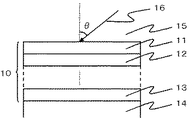
図1に反射防止機能について説明するための多層膜の概念的断面図を示す。多層膜を構成する第1層11の複素屈折率をN1とし、第1層11に波長λのレーザー光16の方向と多層膜基板表面の法線とがなす角度をθとし、第1層11の厚さをd1とすると、第1層11の位相厚さδ1は(1)式で表される。また、求める多層膜の光学アドミッタンスは真空中の光学アドミッタンスで規格化されたものである。
FIG. 1 is a conceptual cross-sectional view of a multilayer film for explaining the antireflection function. The complex refractive index of the

入射媒質14と第1層11との境界の電場をEa、磁場をHaとする。一方、第q−1層13と基板(第q層)14との界面の電場をEs、磁場をHsとする。このとき、(2)式に特性マトリクスの関係を示す。ここでηrは第r層の光学アドミッタンス、δrは第r層の位相厚さである。
The electric field at the boundary between the
(2)式をEsで割って(3)に示す式に変換する。ここでηsは基板14の光学アドミッタンスである。
(2) converting equation in the equation shown in dividing by E s (3). Here, η s is the optical admittance of the
(3)式より、多層膜10の光学アドミッタンスYは(4)で示される。
From the equation (3), the optical admittance Y of the
![]()
![]()
本発明では特定の波長帯(395〜415nm)の光が基板表面に垂直となる方向から入射した場合において、基板と多層膜との光学アドミッタンス、そして多層膜と入射媒質との光学アドミッタンスを実質的に等しくさせるように層を構成することで反射防止膜機能を実現させている。さらに、上記のように同波長帯において1/4波長板として機能させるような層の構成としている。 In the present invention, when light in a specific wavelength band (395 to 415 nm) is incident from a direction perpendicular to the substrate surface, the optical admittance between the substrate and the multilayer film and the optical admittance between the multilayer film and the incident medium are substantially reduced. The antireflection film function is realized by configuring the layers so as to be equal to each other. Further, as described above, the layer is configured to function as a quarter-wave plate in the same wavelength band.
(実施例1)
図2に本発明の実施例1に係る複屈折板の模式的断面図を示す。B270ガラス基板101を洗浄し、充分に乾燥させた後、斜方蒸着膜成膜治具を有する真空蒸着装置にガラス基板を装着しチャンバー内を真空状態とした。蒸着源が基板法線方向から+70度傾斜させた方向となるように治具を固定し、第1工程としてガラス基板上にTa2O5層111(226nm)、SiO2層112(318nm)、Ta2O5層113(140nm)、SiO2層114(10nm)、Ta2O5層115(289nm)の順に斜方蒸着多層膜を形成した。その後第1工程で斜方蒸着させた基板を取り出し、第2工程として蒸着方向が−70度傾斜させた方向となるように基板を装着し、さらにTa2O5層121(140nm)、SiO2層122(160nm)、Ta2O5層123(45nm)、SiO2層124(160nm)、Ta2O5層125(430nm)、SiO2層126(161nm)、Ta2O5層127(40nm)、SiO2層128(236nm)の順に斜方蒸着多層膜を形成した。
(Example 1)
FIG. 2 shows a schematic cross-sectional view of a birefringent plate according to Embodiment 1 of the present invention. After the
以上の第1工程におけるTa2O5の斜方蒸着多層膜の合計の厚さは655nm、第2工程におけるTa2O5の斜方蒸着多層膜の合計の厚さは655nmであり、第1、2工程におけるTa2O5の合計の厚さは等しいものとした。実施例1における複屈折板と接する空気の屈折率は1であり、405nmの波長の光を入射したときの複屈折板の光学アドミッタンスは1.06−i0.06(i:虚数単位)である。また、波長405nmのレーザー光を多層膜上面から照射して透過率を測定したところ、干渉の影響がなく、適正なリタデーションを有するとともに反射防止膜としての機能も同時に有することが確認された。 The total thickness of the oblique deposition multilayer film of Ta 2 O 5 in the first process is 655 nm, and the total thickness of the oblique deposition multilayer film of Ta 2 O 5 in the second process is 655 nm. The total thickness of Ta 2 O 5 in the two steps was assumed to be equal. In Example 1, the refractive index of air in contact with the birefringent plate is 1, and the optical admittance of the birefringent plate when light having a wavelength of 405 nm is incident is 1.06-i0.06 (i: imaginary unit). . Further, when the transmittance was measured by irradiating a laser beam having a wavelength of 405 nm from the upper surface of the multilayer film, it was confirmed that there was no influence of interference, an appropriate retardation, and a function as an antireflection film at the same time.
(実施例2)
図3に本発明の実施例2に係る複屈折板の模式的断面図を示す。実施例1で作成した斜方蒸着多層膜に波長405nmにおいて光学膜厚がλ/2となるように蒸着源の鉛直方向と基板面の法線方向が一致するようにSiO2を正面より蒸着させた膜を形成した。作製した複屈折板をダイシングによって4mm×5mmに切断し60℃、湿度90%の環境下に500時間保管したところ蒸着多層膜の剥離が無いことが確認され、また、SiO2膜により斜方蒸着多層膜表面の保護効果が確認された。
(Example 2)
FIG. 3 shows a schematic cross-sectional view of a birefringent plate according to Embodiment 2 of the present invention. SiO 2 is vapor-deposited from the front so that the vertical direction of the vapor deposition source and the normal direction of the substrate surface coincide with each other so that the optical film thickness is λ / 2 at the wavelength of 405 nm on the oblique vapor deposition multilayer film prepared in Example 1. A film was formed. Fabricated birefringent plate is cut by dicing to 4 mm × 5 mm 60 ° C., it is confirmed peeling of the deposited multilayer was stored for 500 hours under a humidity of 90% for no, also oblique evaporation by SiO 2 film The protective effect of the multilayer film surface was confirmed.
(実施例3)
図5に本発明の実施例3に係る複屈折板の模式的断面図を示す。最初に、図4の概念図に示すように、基板をダイシング装置により幅0.6mm、深さ0.4mm加工溝22を形成した後に洗浄し、充分に乾燥させた。その後、斜方蒸着膜成膜治具を有する真空蒸着装置にガラス基板301を装着しチャンバー内を真空状態とした。蒸着源が基板法線方向から+70度傾斜させた方向となるように治具を固定し、第1工程としてガラス基板上にSiO2層311(14nm)、Ta2O5層312(26nm)、SiO2層313(15nm)、Ta2O5層314(650nm)の順に斜方蒸着多層膜を形成した。その後第1工程で斜方蒸着させた基板を取り出し、第2工程として蒸着方向が−70度傾斜させた方向となるように基板を装着し、さらにTa2O5層321(650nm)、SiO2層322(16nm)、Ta2O5層323(21nm)、SiO2層324(155nm)の順に斜方蒸着多層膜を形成した。
(Example 3)
FIG. 5 shows a schematic cross-sectional view of a birefringent plate according to Embodiment 3 of the present invention. First, as shown in the conceptual diagram of FIG. 4, the substrate was washed with a dicing machine after forming a processed
斜方蒸着膜を上記のような厚さに設定することによって、上記多層斜方蒸着膜の光学アドミッタンスは405nmの波長帯においてSiO2とほぼ等しいものになるため、多層斜方蒸着膜により界面との内部干渉によって生じる反射を低減することでリップルも抑制することができた。以上の斜方蒸着多層膜にCVD装置を用いて厚さ約2μmのSiO2層331を成膜した。成膜後ダイシング装置により加工溝22に沿って幅0.2mmのブレードにより切断した。以上のような工程により斜方蒸着多層膜表面だけではなく斜方蒸着多層膜側面にもSiO2の保護膜をつけることができた。具体的に、保護膜であるSiO2の屈折率は1.48であり、405nmの波長の光を入射したときのガラス基板と斜方蒸着多層膜からなる層の光学アドミッタンスは1.54−i0.04(i:虚数単位)である。また、85℃の環境下に500時間保管して波長405nmのレーザー光を多層膜上面から照射して透過率を測定したところ透過率、リタデーション特性が良好で高耐久性、高信頼性の複屈折板300を得ることができた。
By setting the thickness of the oblique deposition film as described above, the optical admittance of the multilayer oblique deposition film becomes substantially equal to SiO 2 in the wavelength band of 405 nm. Ripple could be suppressed by reducing reflection caused by internal interference. A SiO 2 layer 331 having a thickness of about 2 μm was formed on the above obliquely deposited multilayer film using a CVD apparatus. After the film formation, the wafer was cut along a processed
(実施例4)
図6に本発明の実施例4に係る複屈折板の模式的断面図を示す。実施例3でCVDにより作成した最表層であるSiO2層331の上にさらにTa2O5層401を14nm、SiO2層402を92nmの順に蒸着源の鉛直方向と基板面の法線方向が一致するように正面より蒸着させて反射防止膜を形成した。実施例4における複屈折板と接する空気の屈折率は1であり、405nmの波長の光を入射したときの複屈折板の光学アドミッタンスは1.06+i0.04(i:虚数単位)である。この反射防止膜により、実施例3の構成における405nmの波長帯においてSiO2層331と空気との界面で発生する光の反射を低減させることができ、さらに高透過率の複屈折板400を得ることができた。
Example 4
FIG. 6 shows a schematic cross-sectional view of a birefringent plate according to Example 4 of the present invention. The vertical direction of the evaporation source and the normal direction of the substrate surface are in the order of 14 nm of the Ta 2 O 5 layer 401 and 92 nm of the SiO 2 layer 402 on the SiO 2 layer 331 which is the outermost layer created by CVD in Example 3. An antireflection film was formed by vapor deposition from the front so as to match. In Example 4, the refractive index of air in contact with the birefringent plate is 1, and the optical admittance of the birefringent plate when light having a wavelength of 405 nm is incident is 1.06 + i0.04 (i: imaginary unit). With this antireflection film, reflection of light generated at the interface between the SiO 2 layer 331 and the air in the wavelength band of 405 nm in the configuration of Example 3 can be reduced, and the
(比較例1)
図7に本発明の比較例1に係る複屈折板の模式的断面図を示す。B270ガラス基板501を洗浄し、充分に乾燥させた後、斜方蒸着膜成膜治具を有する真空蒸着装置にガラス基板を装着しチャンバー内を真空状態とした。蒸着源が基板法線方向から+70度傾斜させるように治具を固定し、Ta2O5層502を650nmの厚さとなるように斜方蒸着多層膜を形成した。その後、第1工程で斜方蒸着させた基板を取り出し、第2工程として蒸着方向が−70度傾斜させるように基板を装着し、さらにTa2O5層503を650nmの厚さとなるように斜方蒸着多層膜を形成した。
(Comparative Example 1)
FIG. 7 shows a schematic cross-sectional view of a birefringent plate according to Comparative Example 1 of the present invention. After the
2層の斜方蒸着多層膜が形成された基板の透過率を測定したところ波長405nmの波長帯においてTa2O5多層膜内の干渉による反射率の増大が確認された。 When the transmittance of the substrate on which the two-layer oblique vapor deposition multilayer film was formed was measured, an increase in reflectance due to interference in the Ta 2 O 5 multilayer film was confirmed in the wavelength band of 405 nm.
(比較例2)
図8に本発明の比較例2に係る複屈折板の模式的断面図を示す。比較例1で作成した斜方蒸着多層膜に波長405nmにおいて光学膜厚がλ/2となるように蒸着源の鉛直方向と基板面の法線方向が一致するようにSiO2膜601を正面より蒸着させた膜を形成した。SiO2膜により表面の保護効果が向上したもののTa2O5多層膜内の干渉による反射率の増大が確認された。
(Comparative Example 2)
FIG. 8 shows a schematic cross-sectional view of a birefringent plate according to Comparative Example 2 of the present invention. The SiO 2 film 601 is applied from the front so that the vertical direction of the vapor deposition source and the normal direction of the substrate surface coincide with each other so that the optical film thickness is λ / 2 at the wavelength of 405 nm. A deposited film was formed. Although the protective effect of the surface was improved by the SiO 2 film, an increase in reflectance due to interference in the Ta 2 O 5 multilayer film was confirmed.
本発明によれば、複数層の斜方蒸着膜を形成することによって特定の波長帯に対して良好な1/4波長位相差板となるとともに、複数層の斜方蒸着膜が反射防止膜機能も有する。また、斜方蒸着膜の側面に対して安定した保護膜を形成することが可能となる。したがって、光ヘッド装置などの偏光変換素子等に用いられる複屈折板として有用である。 According to the present invention, by forming a plurality of layers of obliquely deposited films, a favorable quarter-wave retardation film is obtained for a specific wavelength band, and the layers of obliquely deposited films function as antireflection films. Also have. In addition, a stable protective film can be formed on the side surface of the obliquely deposited film. Therefore, it is useful as a birefringent plate used for a polarization conversion element such as an optical head device.
10 多層膜
11 多層膜の第1層
12 多層膜の第2層
13 多層膜の第q−1層
14 基板
15 入射媒体
16 レーザー光入射方向
100、200、300、400、500、600 複屈折板
21、101、301、501 ガラス基板
110、310 第1工程により形成された斜方蒸着膜層
120、320 第2工程により形成された斜方蒸着膜層
111、113、114、115、121、123、125、127、312、314、321、323、502、503 Ta2O5斜方蒸着層
112、114、122、124、126、128、311、313、322、324 SiO2斜方蒸着膜
201、402、311、601 SiO2蒸着層
401 Ta2O5蒸着層
22 加工溝
DESCRIPTION OF
Claims (15)
(a1−1.02n1)2+b1 2<0.04n1 2 When the refractive index of the protective film is n 1 and the optical admittance of the layer including the transparent substrate and the multilayer film is (a 1 + ib 1 ), light having a wavelength of 395 to 415 nm is incident on the substrate perpendicularly. , A 1 , b 1 satisfy the following inequality: The birefringent plate according to claim 6, wherein i represents an imaginary unit.
(A 1 -1.02n 1 ) 2 + b 1 2 <0.04n 1 2
(a2−1.02n2)2+b2 2<0.04n2 2 The refractive index of a medium in contact with the upper surface of the protective film on the multilayer film is n 2, and the optical admittance of the layer including the transparent substrate, the multilayer film, and the protective film is (a 2 + ib 2 ) and is at least 395 to 415 nm The birefringent plate according to claim 8, wherein a 2 and b 2 satisfy the following inequality when light of some wavelengths is incident on the substrate perpendicularly: i indicates an imaginary unit ).
(A 2 -1.02n 2 ) 2 + b 2 2 <0.04n 2 2
(a3−1.02n3)2+b3 2<0.04n3 2 The refractive index of the medium in contact with the upper surface of the antireflection film and n 3, 395~415nm the optical admittance of the layer containing the said transparent substrate multilayer film and the protective film and the antireflection film as (a 3 + ib 3) The birefringent plate (i: imaginary unit) according to claim 12, wherein a 3 and b 3 satisfy the following inequality when light of at least a part of the wavelength is perpendicularly incident on the substrate: ).
(A 3 -1.02n 3 ) 2 + b 3 2 <0.04n 3 2
Priority Applications (1)
| Application Number | Priority Date | Filing Date | Title |
|---|---|---|---|
| JP2007054114A JP2008216644A (en) | 2007-03-05 | 2007-03-05 | Birefringent plate and optical head device |
Applications Claiming Priority (1)
| Application Number | Priority Date | Filing Date | Title |
|---|---|---|---|
| JP2007054114A JP2008216644A (en) | 2007-03-05 | 2007-03-05 | Birefringent plate and optical head device |
Publications (2)
| Publication Number | Publication Date |
|---|---|
| JP2008216644A true JP2008216644A (en) | 2008-09-18 |
| JP2008216644A5 JP2008216644A5 (en) | 2009-09-10 |
Family
ID=39836758
Family Applications (1)
| Application Number | Title | Priority Date | Filing Date |
|---|---|---|---|
| JP2007054114A Pending JP2008216644A (en) | 2007-03-05 | 2007-03-05 | Birefringent plate and optical head device |
Country Status (1)
| Country | Link |
|---|---|
| JP (1) | JP2008216644A (en) |
Cited By (11)
| Publication number | Priority date | Publication date | Assignee | Title |
|---|---|---|---|---|
| US20120295069A1 (en) * | 2011-05-16 | 2012-11-22 | Sony Chemical & Information Device Corporation | Phase difference element |
| WO2014208724A1 (en) * | 2013-06-27 | 2014-12-31 | デクセリアルズ株式会社 | Polarization conversion element, polarization-conversion-element manufacturing method, light-source unit, and optical device |
| JP2015068935A (en) * | 2013-09-27 | 2015-04-13 | デクセリアルズ株式会社 | Retardation element and method for manufacturing the same, liquid crystal display device and method for manufacturing the same, and projection type image display device |
| JP2015082035A (en) * | 2013-10-23 | 2015-04-27 | デクセリアルズ株式会社 | Retardation element and method for manufacturing the same, liquid crystal display device, and projection type image display device |
| JP2015092282A (en) * | 2015-01-20 | 2015-05-14 | デクセリアルズ株式会社 | Manufacturing method for wavelength plate |
| CN106358443A (en) * | 2013-05-28 | 2017-01-25 | 日立造船株式会社 | Polarization imaging filter and method for manufacturing same |
| JP2017138464A (en) * | 2016-02-03 | 2017-08-10 | Jxtgエネルギー株式会社 | Optical retardation member, composite optical member including optical retardation member, and method for manufacturing optical retardation member |
| CN108369311A (en) * | 2016-03-18 | 2018-08-03 | Jxtg能源株式会社 | The manufacturing method of optical phase difference component, the composite optical member for having optical phase difference component and optical phase difference component |
| WO2019102902A1 (en) * | 2017-11-21 | 2019-05-31 | デクセリアルズ株式会社 | Optical element and projection-type image display apparatus |
| WO2021065157A1 (en) * | 2019-10-01 | 2021-04-08 | ソニー株式会社 | Optical compensation element, liquid crystal display device, and electronic apparatus |
| CN113215534A (en) * | 2021-05-07 | 2021-08-06 | 业成科技(成都)有限公司 | Optical element and method for manufacturing the same |
Citations (6)
| Publication number | Priority date | Publication date | Assignee | Title |
|---|---|---|---|---|
| JPH09166710A (en) * | 1995-12-15 | 1997-06-24 | Sano Fuji Koki Kk | Double refractive film and optical system using the same |
| JPH09277395A (en) * | 1996-04-15 | 1997-10-28 | Alps Electric Co Ltd | Production of optical multilayered membrane filter |
| JPH09297214A (en) * | 1996-05-08 | 1997-11-18 | Matsushita Electric Ind Co Ltd | Polarizing element |
| JPH1081955A (en) * | 1996-07-11 | 1998-03-31 | Toyota Central Res & Dev Lab Inc | Diagonally vapor deposited film element and optical device formed by using the same |
| JPH10255313A (en) * | 1997-03-10 | 1998-09-25 | Matsushita Electric Ind Co Ltd | Optical pickup and its manufacture |
| JP2003121603A (en) * | 2001-10-12 | 2003-04-23 | Bridgestone Corp | Antireflection film |
-
2007
- 2007-03-05 JP JP2007054114A patent/JP2008216644A/en active Pending
Patent Citations (6)
| Publication number | Priority date | Publication date | Assignee | Title |
|---|---|---|---|---|
| JPH09166710A (en) * | 1995-12-15 | 1997-06-24 | Sano Fuji Koki Kk | Double refractive film and optical system using the same |
| JPH09277395A (en) * | 1996-04-15 | 1997-10-28 | Alps Electric Co Ltd | Production of optical multilayered membrane filter |
| JPH09297214A (en) * | 1996-05-08 | 1997-11-18 | Matsushita Electric Ind Co Ltd | Polarizing element |
| JPH1081955A (en) * | 1996-07-11 | 1998-03-31 | Toyota Central Res & Dev Lab Inc | Diagonally vapor deposited film element and optical device formed by using the same |
| JPH10255313A (en) * | 1997-03-10 | 1998-09-25 | Matsushita Electric Ind Co Ltd | Optical pickup and its manufacture |
| JP2003121603A (en) * | 2001-10-12 | 2003-04-23 | Bridgestone Corp | Antireflection film |
Cited By (22)
| Publication number | Priority date | Publication date | Assignee | Title |
|---|---|---|---|---|
| US20120295069A1 (en) * | 2011-05-16 | 2012-11-22 | Sony Chemical & Information Device Corporation | Phase difference element |
| US9946001B2 (en) | 2011-05-16 | 2018-04-17 | Dexerials Corporation | Phase difference element having birefringent film containing titanium oxide tantalum oxide |
| US9376744B2 (en) * | 2011-05-16 | 2016-06-28 | Dexerials Corporation | Phase-difference element having birefringent film containing TiO2 and Ta2O5 |
| CN106358443A (en) * | 2013-05-28 | 2017-01-25 | 日立造船株式会社 | Polarization imaging filter and method for manufacturing same |
| JP2015215582A (en) * | 2013-06-27 | 2015-12-03 | デクセリアルズ株式会社 | Polarization conversion element, manufacturing method of polarization conversion element, light source unit and optical device |
| WO2014208724A1 (en) * | 2013-06-27 | 2014-12-31 | デクセリアルズ株式会社 | Polarization conversion element, polarization-conversion-element manufacturing method, light-source unit, and optical device |
| US10042176B2 (en) | 2013-06-27 | 2018-08-07 | Dexerials Corporation | Polarization conversion element, polarization-conversion-element manufacturing method, light-source unit, and optical device |
| JP2015068935A (en) * | 2013-09-27 | 2015-04-13 | デクセリアルズ株式会社 | Retardation element and method for manufacturing the same, liquid crystal display device and method for manufacturing the same, and projection type image display device |
| JP2015082035A (en) * | 2013-10-23 | 2015-04-27 | デクセリアルズ株式会社 | Retardation element and method for manufacturing the same, liquid crystal display device, and projection type image display device |
| JP2015092282A (en) * | 2015-01-20 | 2015-05-14 | デクセリアルズ株式会社 | Manufacturing method for wavelength plate |
| CN108603972A (en) * | 2016-02-03 | 2018-09-28 | Jxtg能源株式会社 | The manufacturing method of optical phase difference component, the composite optical member for having optical phase difference component and optical phase difference component |
| WO2017135220A1 (en) * | 2016-02-03 | 2017-08-10 | Jxエネルギー株式会社 | Optical phase difference member, composite optical member comprising optical phase difference member, and method for producing optical phase difference member |
| JP2017138464A (en) * | 2016-02-03 | 2017-08-10 | Jxtgエネルギー株式会社 | Optical retardation member, composite optical member including optical retardation member, and method for manufacturing optical retardation member |
| TWI711846B (en) * | 2016-02-03 | 2020-12-01 | 日商捷客斯能源股份有限公司 | Optical retardation member, composite optical member with optical retardation member, and manufacturing method of optical retardation member |
| CN108369311A (en) * | 2016-03-18 | 2018-08-03 | Jxtg能源株式会社 | The manufacturing method of optical phase difference component, the composite optical member for having optical phase difference component and optical phase difference component |
| CN108369311B (en) * | 2016-03-18 | 2021-07-16 | Jxtg能源株式会社 | Optical retardation member, composite optical member provided with optical retardation member, and method for producing optical retardation member |
| WO2019102902A1 (en) * | 2017-11-21 | 2019-05-31 | デクセリアルズ株式会社 | Optical element and projection-type image display apparatus |
| JP2019095554A (en) * | 2017-11-21 | 2019-06-20 | デクセリアルズ株式会社 | Optical element and projection type image display device |
| US11294114B2 (en) | 2017-11-21 | 2022-04-05 | Dexerials Corporation | Optical element and projection image display apparatus |
| US11573362B2 (en) | 2017-11-21 | 2023-02-07 | Dexerials Corporation | Optical element and projection image display apparatus |
| WO2021065157A1 (en) * | 2019-10-01 | 2021-04-08 | ソニー株式会社 | Optical compensation element, liquid crystal display device, and electronic apparatus |
| CN113215534A (en) * | 2021-05-07 | 2021-08-06 | 业成科技(成都)有限公司 | Optical element and method for manufacturing the same |
Similar Documents
| Publication | Publication Date | Title |
|---|---|---|
| JP2008216644A (en) | Birefringent plate and optical head device | |
| KR100642951B1 (en) | Optical head device and production method thereof | |
| JP2008216644A5 (en) | ||
| JP5223236B2 (en) | Objective lens and optical pickup device | |
| JP5353666B2 (en) | Wire grid polarizer and optical head device | |
| JP2006073042A (en) | Diffraction element and optical head device | |
| JP2011187139A (en) | Grating element and method for manufacturing the same, and optical pickup device using the grating element | |
| US20090110011A1 (en) | Optical component for laser beam | |
| WO2011148465A1 (en) | Wave plate and wave plate manufacturing method | |
| US20140044940A1 (en) | Optical recording medium and method for manufacturing optical recording medium | |
| JP2012243378A (en) | Optical element and optical head device | |
| JP4218240B2 (en) | Optical head device | |
| JP4314480B2 (en) | Diffraction element and optical head device | |
| JP2003222707A (en) | Optical lens and optical information recording reproduction device | |
| JP5234151B2 (en) | Diffraction element and optical head device | |
| JP5082792B2 (en) | Optical head device | |
| JP2004296041A (en) | Optical head device | |
| JP2012119046A (en) | Lens and optical information recording/reproducing device | |
| JP4139140B2 (en) | Polarization hologram element and manufacturing method thereof | |
| JP3947828B2 (en) | Optical head device and manufacturing method thereof | |
| JP2005339595A (en) | Optical head device | |
| JP2013077374A (en) | Diffraction element and optical head unit | |
| JP2004341471A (en) | Diffraction element and optical head system | |
| JP5508295B2 (en) | 1/4 wave plate for optical pickup | |
| JP2007034030A (en) | Liquid crystal device |
Legal Events
| Date | Code | Title | Description |
|---|---|---|---|
| A521 | Written amendment |
Free format text: JAPANESE INTERMEDIATE CODE: A523 Effective date: 20090729 |
|
| A621 | Written request for application examination |
Free format text: JAPANESE INTERMEDIATE CODE: A621 Effective date: 20090904 |
|
| A977 | Report on retrieval |
Free format text: JAPANESE INTERMEDIATE CODE: A971007 Effective date: 20110202 |
|
| A131 | Notification of reasons for refusal |
Free format text: JAPANESE INTERMEDIATE CODE: A131 Effective date: 20110329 |
|
| RD02 | Notification of acceptance of power of attorney |
Free format text: JAPANESE INTERMEDIATE CODE: A7422 Effective date: 20110411 |
|
| A521 | Written amendment |
Free format text: JAPANESE INTERMEDIATE CODE: A523 Effective date: 20110519 |
|
| A02 | Decision of refusal |
Free format text: JAPANESE INTERMEDIATE CODE: A02 Effective date: 20120306 |