JP2008123610A - Optical information recording medium and method of manufacturing the same - Google Patents
Optical information recording medium and method of manufacturing the same Download PDFInfo
- Publication number
- JP2008123610A JP2008123610A JP2006306203A JP2006306203A JP2008123610A JP 2008123610 A JP2008123610 A JP 2008123610A JP 2006306203 A JP2006306203 A JP 2006306203A JP 2006306203 A JP2006306203 A JP 2006306203A JP 2008123610 A JP2008123610 A JP 2008123610A
- Authority
- JP
- Japan
- Prior art keywords
- substrate
- layer
- optical information
- information recording
- recording medium
- Prior art date
- Legal status (The legal status is an assumption and is not a legal conclusion. Google has not performed a legal analysis and makes no representation as to the accuracy of the status listed.)
- Pending
Links
Images


Landscapes
- Optical Record Carriers And Manufacture Thereof (AREA)
- Manufacturing Optical Record Carriers (AREA)
Abstract
Description
本発明は、ブルーレイディスク等の次世代光情報記録媒体に用いられる基板形状と、それを用いた光情報記録媒体の製造方法に関する。 The present invention relates to a substrate shape used for a next-generation optical information recording medium such as a Blu-ray disc, and a method for manufacturing an optical information recording medium using the same.
情報記録媒体として、光ディスク等の光情報記録媒体が急速に普及しつつある。このような光情報記録媒体としては、CD−R等のような、厚さ1.2mm(直径120mmまたは80mm)の光透過性の樹脂基板上に反射層及び記録層を形成したものがある。近年、さらに高い情報記録密度が要求されてきている。そこで、レーザ波長を短く且つ開口数(NA:numerical aperture)の大きな対物レンズを使用する方式が考えられ、DVD±R等のような光情報記録媒体が実現されている。このDVD±Rは、短波長化と高NA化によるディスクの傾き角度(チルト)の許容値を大きくするために、厚さ0.6mmの光透過性の樹脂基板を2枚貼り合せ、この基板間に反射層及び記録層を挟んだ構造を有している。 As information recording media, optical information recording media such as optical discs are rapidly spreading. As such an optical information recording medium, there is one in which a reflective layer and a recording layer are formed on a light transmissive resin substrate having a thickness of 1.2 mm (diameter 120 mm or 80 mm) such as a CD-R. In recent years, higher information recording density has been demanded. Therefore, a method of using an objective lens having a short laser wavelength and a large numerical aperture (NA) is conceivable, and an optical information recording medium such as a DVD ± R is realized. This DVD ± R is bonded to two optically transmissive resin substrates having a thickness of 0.6 mm in order to increase the allowable value of the tilt angle (tilt) of the disc by shortening the wavelength and increasing the NA. The reflective layer and the recording layer are sandwiched between them.
しかし、近年では高精細な映像データを記録するために、さらに高い情報記録密度が要求されてきている。そこで、ブルーレイディスクのように、厚さ1.1mmの樹脂基板の光入射面側に反射層及び記録層を形成してこの記録層を厚さ0.1mmの光透過性のカバー層で覆う構造の光情報記録媒体が提案されている。 However, in recent years, a higher information recording density has been required in order to record high-definition video data. Therefore, like Blu-ray Disc, a structure in which a reflective layer and a recording layer are formed on the light incident surface side of a resin substrate having a thickness of 1.1 mm and this recording layer is covered with a light-transmitting cover layer having a thickness of 0.1 mm. Optical information recording media have been proposed.
このような光情報記録媒体の場合、カバー層を形成するには、特許第3726759号公報や特開2004−288270号公報に開示されているように、光透過性の紫外線硬化樹脂または放射線硬化樹脂をスピンコート法によって形成する方法が提案されている。この方法は、センターキャップで基板中心部の貫通孔を塞いで、この基板中心部にノズル等で硬化性樹脂を供給してスピンコートで延伸塗布する方法である。硬化性樹脂は硬化前の粘度が1000〜3000cpsと比較的高いので、カバー層の厚みを均一にするには、基板を静止状態または比較的低速(例えば60rpm)で回転させながら硬化性樹脂を供給して一旦中心部に滞留させ、その後高速(例えば5000rpm)で回転させて延伸塗布する必要がある。 In the case of such an optical information recording medium, in order to form a cover layer, as disclosed in Japanese Patent No. 3726759 and Japanese Patent Application Laid-Open No. 2004-288270, a light transmissive ultraviolet curable resin or radiation curable resin is used. There has been proposed a method of forming a film by spin coating. This method is a method in which a through hole at the center of the substrate is closed with a center cap, a curable resin is supplied to the center of the substrate with a nozzle or the like, and stretch coating is performed by spin coating. Since the viscosity of the curable resin before curing is relatively high at 1000 to 3000 cps, in order to make the thickness of the cover layer uniform, the curable resin is supplied while rotating the substrate in a stationary state or at a relatively low speed (for example, 60 rpm). Then, it is necessary to make it stay in the center and then apply it by stretching at a high speed (for example, 5000 rpm).
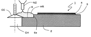
このような方法では、回転させて延伸塗布するまでは硬化性樹脂が基板中心部に滞留させて、基板を回転させた際には周方向で樹脂量のバラツキがないように、すなわち略同心円状に硬化性樹脂が延伸塗布されることが望ましい。しかしながら、実際にはセンターキャップにある程度の傾斜がついており、硬化性樹脂も塗布厚みを均一にするために必要量に加えてある程度の余分の量が供給されるため、時間と共に硬化性樹脂が半径方向に拡がってしまう。また、硬化性樹脂は比較的粘度が高いため、ノズルからの吐出に時間がかかるので、図7に示すように硬化性樹脂HRの拡がりにバラツキが生じてしまう。 In such a method, the curable resin stays in the center of the substrate until it is rotated and stretched, and when the substrate is rotated, there is no variation in the resin amount in the circumferential direction, that is, substantially concentric. It is desirable that the curable resin is stretched and applied. However, the center cap is actually inclined to some extent, and the curable resin is supplied with a certain amount of extra amount in addition to the necessary amount to make the coating thickness uniform. It spreads in the direction. In addition, since the curable resin has a relatively high viscosity, it takes time to discharge from the nozzle, and thus the spread of the curable resin HR varies as shown in FIG.
このような状態で基板2‘を回転させて延伸塗布を行った場合、図8に示すように遠心力のかかり方が不均等になり、硬化性樹脂HRの伸ばされ方にバラツキが生じる。このようになると、硬化性樹脂HRの厚みが周方向でバラツキを生じてしまう。カバー層は記録光または再生光が通過する関係上その厚みのバラツキの許容差は例えばブルーレイディスクでは±2μm程度である。従来の手法ではその許容差を超えたバラツキを生じてしまうという問題があった。 When the substrate 2 'is rotated and applied in such a state as shown in FIG. 8, the application of centrifugal force becomes uneven as shown in FIG. 8, and the method of extending the curable resin HR varies. In this case, the thickness of the curable resin HR varies in the circumferential direction. Since the cover layer allows recording light or reproduction light to pass therethrough, the tolerance of variation in thickness thereof is, for example, about ± 2 μm for a Blu-ray disc. The conventional method has a problem that the variation exceeds the tolerance.
本発明は、硬化性樹脂の供給時の拡がりを抑え、カバー層の厚みのバラツキを低減することができる光情報記録媒体の製造方法と、この方法を実現するための基板を用いた光情報記録媒体を提案するものである。 The present invention relates to a method for manufacturing an optical information recording medium capable of suppressing the spread at the time of supplying a curable resin and reducing the variation in the thickness of the cover layer, and an optical information recording using a substrate for realizing the method. It proposes a medium.
本発明では第一の技術手段として、中心部分に貫通孔を有する円形の基板と、前記基板の光入射側となる一方の面側に形成された反射層及び記録層と、前記反射層及び前記記録層が形成された面上に設けられた光透過性のカバー層と、を有する光情報記録媒体において、前記基板は、光入射側の貫通孔近傍領域が凹部になるように、前記貫通孔近傍領域の基板厚みが、前記反射層及び前記記録層が形成されている領域の基板厚みよりも薄いことを特徴とする光情報記録媒体を提案する。 In the present invention, as a first technical means, a circular substrate having a through-hole in a central portion, a reflective layer and a recording layer formed on one side of the substrate which is a light incident side, the reflective layer and the In the optical information recording medium having a light-transmitting cover layer provided on the surface on which the recording layer is formed, the substrate has the through hole so that a region near the through hole on the light incident side becomes a recess. Proposed is an optical information recording medium characterized in that the substrate thickness in the vicinity region is thinner than the substrate thickness in the region where the reflective layer and the recording layer are formed.
上記第一の技術手段によれば、貫通孔近傍の凹部によって硬化性樹脂の拡がりを抑えることができ、スピンコートによって均等に延伸塗布が行われるので、カバー層の厚みのバラツキが低減された光情報記録媒体を得ることができるものである。なお、貫通孔近傍とは、貫通孔の縁から基板の半径11.5mm以内の領域のことを指す。すなわち前記凹部は貫通孔と中心点を共有する直径23mm以内の円形の凹部となる。 According to the first technical means described above, the spread of the curable resin can be suppressed by the recesses in the vicinity of the through-holes, and the stretch coating is performed uniformly by spin coating, so that the light with reduced variation in the thickness of the cover layer is reduced. An information recording medium can be obtained. The vicinity of the through hole refers to a region within a radius of 11.5 mm of the substrate from the edge of the through hole. That is, the concave portion is a circular concave portion having a diameter of 23 mm or less sharing a central point with the through hole.
また、本発明では第ニの技術手段として、前記凹部の段差部分が傾斜面になっていることを特徴とする光情報記録媒体を提案する。この第二の技術手段によれば、スピンコート時に、凹部に滞留させた硬化性樹脂がスムーズに流れ出させることができる。これにより均等な延伸塗布が可能になる。 In the present invention, as a second technical means, an optical information recording medium is proposed in which the step portion of the recess is an inclined surface. According to the second technical means, at the time of spin coating, the curable resin retained in the recesses can flow out smoothly. This makes it possible to apply uniform stretching.
また、本発明では中心部分に貫通孔を有しかつ光入射側となる一方の面上に反射層及び記録層が形成された円形の基板を用意するステップと、前記基板の貫通孔をセンターキャップで塞いで光入射面側の貫通孔近傍領域に光透過性の硬化性樹脂を供給するステップと、前記基板を回転させてスピンコート法によって前記反射層及び前記記録層が形成された面上を前記硬化性樹脂で被覆するステップと、前記硬化性樹脂を硬化させてカバー層を形成するステップと、を有する光情報記録媒体の製造方法において、前記基板として、光入射側の貫通孔近傍領域が凹部になるように、前記貫通孔近傍領域の基板厚みが、前記反射層及び前記記録層が形成されている領域の基板厚みよりも薄くされている基板を用いることを特徴とする光情報記録媒体の製造方法を提案する。 According to the present invention, there is provided a step of preparing a circular substrate having a through hole in the central portion and having a reflective layer and a recording layer formed on one surface on the light incident side, and the through hole of the substrate is provided with a center cap. And supplying a light-transmitting curable resin to the region near the through-hole on the light incident surface side, and rotating the substrate to spin the coating on the surface on which the reflective layer and the recording layer are formed. In the method for manufacturing an optical information recording medium, comprising: coating with the curable resin; and curing the curable resin to form a cover layer. An optical information recording medium using a substrate in which the thickness of the substrate in the vicinity of the through hole is thinner than the thickness of the substrate in the region where the reflective layer and the recording layer are formed so as to form a recess. We propose a method for manufacturing.
この製造方法によれば、硬化性樹脂の供給時の拡がりを抑えることができ、カバー層の厚みのバラツキが低減された光情報記録媒体を製造することができる。 According to this manufacturing method, it is possible to suppress the spread at the time of supplying the curable resin, and it is possible to manufacture an optical information recording medium in which the variation in the thickness of the cover layer is reduced.
本発明によれば、硬化性樹脂の供給時の拡がりを抑え、均等に延伸塗布することができるので、カバー層の厚みのバラツキが低減された光情報記録媒体を得ることができる。 According to the present invention, since the spread at the time of supplying the curable resin can be suppressed and the coating can be uniformly applied, an optical information recording medium in which the variation in the thickness of the cover layer is reduced can be obtained.
本発明の光情報記録媒体に係る実施の形態を、単層の光ディスクの場合を例にとって、図面に基づいて説明する。図1は本発明の光情報記録媒体の中心線より向かって右半分の模式断面図である。この光情報記録媒体1は、中央部分に回転の中心となる貫通孔CHを有する円形の基板2と、基板2の光入射側となる面上に形成された反射層3と、この反射層3の上に形成された記録層4と、この記録層4の上に設けられた光透過性のカバー層5と、を有している。
An embodiment of the optical information recording medium of the present invention will be described with reference to the drawings, taking a single-layer optical disk as an example. FIG. 1 is a schematic cross-sectional view of the right half from the center line of the optical information recording medium of the present invention. The optical
基板2は、反射層3及び記録層4が形成されている部分の厚みtが1.1mmを有する直径120mmの樹脂製の基板である。この基板2には、従来の光情報記録媒体の基板材料として用いられている各種の材料を任意に選択して使用することができる。具体的には、ポリカーボネート、ポリメチルメタクリレート等のアクリル樹脂、ポリ塩化ビニル、塩化ビニル共重合体等の塩化ビニル系樹脂、エポキシ樹脂、アモルファスポリオレフィン、ポリエステル樹脂、アルミニウム等の金属、ガラス等を挙げることができ、必要によりこれらを併用してもよい。上記材料の中では、成型性、耐湿性、寸法安定性及び低価格等の点から熱可塑性樹脂が好ましく、ポリカーボネートが特に好ましい。
The
この基板2は、貫通孔CHの近傍領域の厚みt‘が反射層3及び記録層4の形成部分の厚みtよりも薄くなっており、光入射側の面すなわち記録層4が形成されている面に凹部6が形成されている。基板2の中心線から凹部6の段差部分6a上端までの距離Lは、最大で11.5mmであり、凹部5はこの半径Lの領域内に形成される。凹部6の深さdは50μm〜300μmであり、200μm程度が好ましい。
In this
反射層3は、AgやAl等の金属薄膜で形成されており、記録層4はシアニン系またはアゾ系等の色素を有する層で構成されている。なお、記録層4は書き換え可能な光情報記録媒体にするために色素層に変えて相変化型の薄膜を用いてもよい。また、図1では単層の記録層になっているが、半透過反射層を用いて、例えば光入射側から第一の記録層−半透過反射層−第二の記録層−反射層の順に形成された多層構造の記録層にしてもよい。また、記録特性等の調整、接着性向上あるいは記録層3の保護のための層を、基板2と反射層3の間、反射層3と記録層4の間あるいは記録層4とカバー層5の間に形成しても良い。
The reflection layer 3 is formed of a metal thin film such as Ag or Al, and the recording layer 4 is formed of a layer having a dye such as cyanine or azo. The recording layer 4 may be a phase change type thin film instead of the dye layer in order to make a rewritable optical information recording medium. In FIG. 1, the recording layer is a single layer, but using a transflective layer, for example, from the light incident side in the order of the first recording layer-semi-transmissive reflective layer-second recording layer-reflective layer. The formed recording layer may have a multilayer structure. Further, a layer for adjusting recording characteristics, improving adhesiveness or protecting the recording layer 3 is provided between the
カバー層5は、光透過性の樹脂で形成されており、紫外線または放射線によって硬化する硬化性樹脂が用いられている。この硬化性樹脂は硬化前の粘度が1000〜3000cps程度で、2000cps程度が好ましく、光透過率が、硬化後の厚み0.1mmで、405nmの波長の光にて分光光度計で測定したときに70%以上好ましくは80%以上である。この硬化性樹脂をスピンコート法によって記録層4上での厚みが0.1mmになるように塗布することによってカバー層5が形成される。なお、図1ではカバー層5の表面を便宜上平坦に描いているが、実際には凹部6による凹みが形成されている場合もある。
The cover layer 5 is formed of a light transmissive resin, and a curable resin that is cured by ultraviolet rays or radiation is used. This curable resin has a viscosity before curing of about 1000 to 3000 cps, preferably about 2000 cps, and has a light transmittance of 0.1 mm after curing and a spectrophotometer measured with light having a wavelength of 405 nm. 70% or more, preferably 80% or more. The cover layer 5 is formed by applying this curable resin by spin coating so that the thickness on the recording layer 4 is 0.1 mm. In FIG. 1, the surface of the cover layer 5 is drawn flat for convenience, but a dent due to the
次に、このような光情報記録媒体1の製造方法について説明する。まず、射出成形にて直径120mm、厚さ1.1mmで、中央に直径15mmの貫通孔CH及び直径23mmで深さ200μmの凹部5を有するポリカーボネートのディスク基板2を形成する。この基板2の凹部6が形成されている面上の半径21mm〜58.5mmの領域に、スパッタによってAl金属を付着させ、反射層3を形成する。次に、この反射層3上に、スピンコート法によってシアニン系色素溶液を塗布して記録層4を形成する。
Next, a method for manufacturing such an optical
このようにして反射層3及び記録層4が形成された基板2を用意し、図2に示すように、スピンコータの回転テーブル(図示せず)に前記基板2を載せ、貫通孔CHをセンターキャップCCで塞ぐ。次にノズルNZから粘度2000cpsの光透過性の紫外線硬化性樹脂HRを吐出して、凹部6内に供給する。このとき、回転テーブルを60rpmの比較的低速で回転させながら供給する。なお、ノズルNZを複数(好ましくは3個以上)にするか、ノズルNZを移動させるようにすれば、回転テーブルを静止した状態でもよい。供給された硬化性樹脂HRは段差部分6aによってせき止められるため、図4に示すように、円形に滞留される。
Thus, the
必要量+αの硬化性樹脂HRを供給した後、回転テーブルを5000rpmの高速で回転させる。これによって硬化性樹脂HRは段差部分6aを乗り越えて流れ出し、反射層3及び記録層4を被覆する。このとき硬化性樹脂HRには遠心力が均等にかかるので、図5に示すように、略同心円状に拡がって塗布される。塗布後、紫外線を照射して硬化性樹脂HRを硬化させる。このようにして、厚さ0.1mmのカバー層5が形成される。なお、カバー層の厚みは、硬化性樹脂HRの粘度、回転テーブルの回転速度の他、回転テーブルの回転の加速度によって制御することができるので、厚さを0.1mmにするために適宜条件を設定できる。こうして得られた光情報記録媒体1のカバー層厚みは、バラツキが±2μmのほぼ均一な厚みになる。
After supplying the necessary amount + α of the curable resin HR, the rotary table is rotated at a high speed of 5000 rpm. As a result, the curable resin HR flows over the
なお、図6に示すように段差部分6aを傾斜面にしてもよい。このような形状であれば、スピンコート時に硬化性樹脂HRをスムーズに流れ出させることができる。図6(a)のように断面で見て直線的な傾斜でも良いが、図6(b)〜(d)にあるように、断面で見てR形状になるようにすると、より効果が高い。特に図6(c)及び図6(d)にあるように、段差部分6aの上部がR形状であれば、硬化性樹脂HRをよりスムーズに流れ出させることができる。
In addition, as shown in FIG. 6, you may make the level | step-
以上、本発明の実施形態について説明したが、製造条件や各種寸法等は任意であり、本発明の範囲内であれば適宜調整可能である。 The embodiment of the present invention has been described above, but manufacturing conditions, various dimensions, and the like are arbitrary, and can be appropriately adjusted within the scope of the present invention.
1 光情報記録媒体
2、2‘ 基板
3 反射層
4 記録層
5 カバー層
6 凹部
6a 段差部分
DESCRIPTION OF
Claims (3)
前記基板は、光入射側の貫通孔近傍領域が凹部になるように、前記貫通孔近傍領域の基板厚みが、前記反射層及び前記記録層が形成されている領域の基板厚みよりも薄い
ことを特徴とする光情報記録媒体。 Provided on a circular substrate having a through-hole in the central portion, a reflective layer and a recording layer formed on one side of the substrate on the light incident side, and a surface on which the reflective layer and the recording layer are formed An optical information recording medium having a light-transmitting cover layer,
The substrate is such that the substrate thickness in the region near the through hole is thinner than the region in which the reflective layer and the recording layer are formed so that the region near the through hole on the light incident side becomes a recess. A characteristic optical information recording medium.
前記基板の貫通孔をセンターキャップで塞いで光入射面側の貫通孔近傍領域に光透過性の硬化性樹脂を供給するステップと、
前記基板を回転させてスピンコート法によって前記反射層及び前記記録層が形成された面上を前記硬化性樹脂で被覆するステップと、
前記硬化性樹脂を硬化させてカバー層を形成するステップと、を有する光情報記録媒体の製造方法において、
前記基板として、光入射側の貫通孔近傍領域が凹部になるように、前記貫通孔近傍領域の基板厚みが、前記反射層及び前記記録層が形成されている領域の基板厚みよりも薄くされている基板を用いる
ことを特徴とする光情報記録媒体の製造方法。
Providing a circular substrate having a through hole in the central portion and having a reflective layer and a recording layer formed on one surface on the light incident side;
Filling the through hole of the substrate with a center cap and supplying a light-transmitting curable resin to a region near the through hole on the light incident surface side;
Covering the surface on which the reflective layer and the recording layer are formed by spin coating and rotating the substrate with the curable resin;
Curing the curable resin to form a cover layer, and a method of manufacturing an optical information recording medium comprising:
As the substrate, the substrate thickness in the region near the through hole is made thinner than the region in which the reflective layer and the recording layer are formed so that the region near the through hole on the light incident side becomes a recess. A method for manufacturing an optical information recording medium, comprising using a substrate.
Priority Applications (1)
| Application Number | Priority Date | Filing Date | Title |
|---|---|---|---|
| JP2006306203A JP2008123610A (en) | 2006-11-13 | 2006-11-13 | Optical information recording medium and method of manufacturing the same |
Applications Claiming Priority (1)
| Application Number | Priority Date | Filing Date | Title |
|---|---|---|---|
| JP2006306203A JP2008123610A (en) | 2006-11-13 | 2006-11-13 | Optical information recording medium and method of manufacturing the same |
Publications (2)
| Publication Number | Publication Date |
|---|---|
| JP2008123610A true JP2008123610A (en) | 2008-05-29 |
| JP2008123610A5 JP2008123610A5 (en) | 2009-12-24 |
Family
ID=39508198
Family Applications (1)
| Application Number | Title | Priority Date | Filing Date |
|---|---|---|---|
| JP2006306203A Pending JP2008123610A (en) | 2006-11-13 | 2006-11-13 | Optical information recording medium and method of manufacturing the same |
Country Status (1)
| Country | Link |
|---|---|
| JP (1) | JP2008123610A (en) |
Cited By (2)
| Publication number | Priority date | Publication date | Assignee | Title |
|---|---|---|---|---|
| JP2014053067A (en) * | 2012-08-09 | 2014-03-20 | Panasonic Corp | Disk of information recording medium, disk cartridge, and information recording and reproducing device |
| CN104221086A (en) * | 2012-03-28 | 2014-12-17 | 松下电器产业株式会社 | Disk |
Citations (4)
| Publication number | Priority date | Publication date | Assignee | Title |
|---|---|---|---|---|
| JPS62222449A (en) * | 1986-03-20 | 1987-09-30 | Fuji Photo Film Co Ltd | Substrate for information recording medium |
| JPH0235333A (en) * | 1988-07-25 | 1990-02-05 | Nippon Cement Co Ltd | Bulk-density measuring apparatus |
| JP2006059454A (en) * | 2004-08-20 | 2006-03-02 | Sony Disc & Digital Solutions Inc | Manufacture apparatus and method of optical recording medium |
| JP2006099896A (en) * | 2004-09-30 | 2006-04-13 | Tdk Corp | Manufacturing method of optical disk |
-
2006
- 2006-11-13 JP JP2006306203A patent/JP2008123610A/en active Pending
Patent Citations (4)
| Publication number | Priority date | Publication date | Assignee | Title |
|---|---|---|---|---|
| JPS62222449A (en) * | 1986-03-20 | 1987-09-30 | Fuji Photo Film Co Ltd | Substrate for information recording medium |
| JPH0235333A (en) * | 1988-07-25 | 1990-02-05 | Nippon Cement Co Ltd | Bulk-density measuring apparatus |
| JP2006059454A (en) * | 2004-08-20 | 2006-03-02 | Sony Disc & Digital Solutions Inc | Manufacture apparatus and method of optical recording medium |
| JP2006099896A (en) * | 2004-09-30 | 2006-04-13 | Tdk Corp | Manufacturing method of optical disk |
Cited By (4)
| Publication number | Priority date | Publication date | Assignee | Title |
|---|---|---|---|---|
| CN104221086A (en) * | 2012-03-28 | 2014-12-17 | 松下电器产业株式会社 | Disk |
| JPWO2013145523A1 (en) * | 2012-03-28 | 2015-12-10 | パナソニックIpマネジメント株式会社 | disk |
| CN104221086B (en) * | 2012-03-28 | 2017-05-10 | 松下电器产业株式会社 | Disk |
| JP2014053067A (en) * | 2012-08-09 | 2014-03-20 | Panasonic Corp | Disk of information recording medium, disk cartridge, and information recording and reproducing device |
Similar Documents
| Publication | Publication Date | Title |
|---|---|---|
| JP4262707B2 (en) | Optical information recording medium and method of manufacturing optical information recording medium | |
| CN1655265B (en) | Method of manufacturing optical information recording medium | |
| US7161893B2 (en) | Stamper for fabrication of optical recording medium, method of forming information recording area and light transmissive layer, and optical recording medium | |
| JP4097598B2 (en) | Manufacturing method of optical information recording medium | |
| WO2005018901A1 (en) | Mold, substrate for optical disk, and optical disk | |
| CN1739152A (en) | Method of manufacturing an optical data storage medium, optical data storage medium and apparatus for performing said method | |
| WO2012105724A1 (en) | Optical information recording medium and production method therefor | |
| JP2008123610A (en) | Optical information recording medium and method of manufacturing the same | |
| JP5030607B2 (en) | Optical information recording medium and manufacturing method thereof | |
| JP3955867B2 (en) | Manufacturing method of optical information recording medium | |
| WO2006028051A1 (en) | Method for producing optical information recording medium and optical information recording medium | |
| JP4714703B2 (en) | Optical information recording medium manufacturing method and optical information recording medium | |
| JP2005056503A (en) | Spin coating method and apparatus, method and apparatus for manufacturing optical recording medium, and optical recording medium | |
| JP2009020975A (en) | Multilayer optical recording medium and manufacturing method therefor | |
| JP4656013B2 (en) | Manufacturing method of optical disk medium | |
| JP2005071571A (en) | Optical information recording medium and its manufacturing method | |
| JP6445919B2 (en) | Optical disc and manufacturing method thereof | |
| JP3709349B2 (en) | Optical disc substrate, optical disc | |
| JP4783193B2 (en) | Coating film forming method | |
| JP2008186509A (en) | Optical information recording medium and its manufacturing method | |
| JP2006286076A (en) | Manufacturing method of optical disk, and optical disk | |
| WO2010116945A1 (en) | Multilayer optical information recording medium | |
| JP2007115317A (en) | Optical disk and its manufacturing method | |
| JP2004039168A (en) | Optical disk | |
| JP2004164727A (en) | Method for manufacturing optical recording medium |
Legal Events
| Date | Code | Title | Description |
|---|---|---|---|
| A521 | Request for written amendment filed |
Free format text: JAPANESE INTERMEDIATE CODE: A523 Effective date: 20091106 |
|
| A621 | Written request for application examination |
Free format text: JAPANESE INTERMEDIATE CODE: A621 Effective date: 20091106 |
|
| A977 | Report on retrieval |
Free format text: JAPANESE INTERMEDIATE CODE: A971007 Effective date: 20101130 |
|
| A131 | Notification of reasons for refusal |
Free format text: JAPANESE INTERMEDIATE CODE: A131 Effective date: 20101203 |
|
| A02 | Decision of refusal |
Free format text: JAPANESE INTERMEDIATE CODE: A02 Effective date: 20110325 |