JP4714703B2 - Optical information recording medium manufacturing method and optical information recording medium - Google Patents
Optical information recording medium manufacturing method and optical information recording medium Download PDFInfo
- Publication number
- JP4714703B2 JP4714703B2 JP2007055099A JP2007055099A JP4714703B2 JP 4714703 B2 JP4714703 B2 JP 4714703B2 JP 2007055099 A JP2007055099 A JP 2007055099A JP 2007055099 A JP2007055099 A JP 2007055099A JP 4714703 B2 JP4714703 B2 JP 4714703B2
- Authority
- JP
- Japan
- Prior art keywords
- layer
- substrate
- groove
- recording medium
- information recording
- Prior art date
- Legal status (The legal status is an assumption and is not a legal conclusion. Google has not performed a legal analysis and makes no representation as to the accuracy of the status listed.)
- Expired - Fee Related
Links
- 230000003287 optical effect Effects 0.000 title claims description 75
- 238000004519 manufacturing process Methods 0.000 title claims description 14
- 239000000758 substrate Substances 0.000 claims description 80
- 230000002093 peripheral effect Effects 0.000 claims description 77
- 230000005540 biological transmission Effects 0.000 claims description 51
- 239000011347 resin Substances 0.000 claims description 20
- 229920005989 resin Polymers 0.000 claims description 20
- 239000000463 material Substances 0.000 claims description 19
- 238000000034 method Methods 0.000 claims description 18
- 238000004528 spin coating Methods 0.000 claims description 16
- 230000001678 irradiating effect Effects 0.000 claims description 3
- 239000010410 layer Substances 0.000 description 137
- 238000000576 coating method Methods 0.000 description 38
- 239000011248 coating agent Substances 0.000 description 37
- 239000000975 dye Substances 0.000 description 10
- 239000011241 protective layer Substances 0.000 description 10
- 239000000047 product Substances 0.000 description 9
- 239000000243 solution Substances 0.000 description 9
- 239000007788 liquid Substances 0.000 description 6
- 239000012043 crude product Substances 0.000 description 5
- 238000004544 sputter deposition Methods 0.000 description 5
- 229910052751 metal Inorganic materials 0.000 description 4
- 239000002184 metal Substances 0.000 description 4
- 238000000465 moulding Methods 0.000 description 4
- 229910004298 SiO 2 Inorganic materials 0.000 description 3
- 238000001746 injection moulding Methods 0.000 description 3
- 150000002739 metals Chemical class 0.000 description 3
- 239000002904 solvent Substances 0.000 description 3
- 235000005811 Viola adunca Nutrition 0.000 description 2
- 240000009038 Viola odorata Species 0.000 description 2
- 235000013487 Viola odorata Nutrition 0.000 description 2
- 235000002254 Viola papilionacea Nutrition 0.000 description 2
- 229910045601 alloy Inorganic materials 0.000 description 2
- 239000000956 alloy Substances 0.000 description 2
- 229910052782 aluminium Inorganic materials 0.000 description 2
- 230000000052 comparative effect Effects 0.000 description 2
- 230000006866 deterioration Effects 0.000 description 2
- 230000000694 effects Effects 0.000 description 2
- 229920000515 polycarbonate Polymers 0.000 description 2
- 239000004417 polycarbonate Substances 0.000 description 2
- 239000004925 Acrylic resin Substances 0.000 description 1
- 229920000178 Acrylic resin Polymers 0.000 description 1
- 229910001316 Ag alloy Inorganic materials 0.000 description 1
- BZHJMEDXRYGGRV-UHFFFAOYSA-N Vinyl chloride Chemical compound ClC=C BZHJMEDXRYGGRV-UHFFFAOYSA-N 0.000 description 1
- XAGFODPZIPBFFR-UHFFFAOYSA-N aluminium Chemical compound [Al] XAGFODPZIPBFFR-UHFFFAOYSA-N 0.000 description 1
- 239000000987 azo dye Substances 0.000 description 1
- 239000011230 binding agent Substances 0.000 description 1
- 230000015556 catabolic process Effects 0.000 description 1
- 238000004590 computer program Methods 0.000 description 1
- 229920001577 copolymer Polymers 0.000 description 1
- 229910052802 copper Inorganic materials 0.000 description 1
- 230000003247 decreasing effect Effects 0.000 description 1
- 238000006731 degradation reaction Methods 0.000 description 1
- 238000001035 drying Methods 0.000 description 1
- 239000003822 epoxy resin Substances 0.000 description 1
- 239000011521 glass Substances 0.000 description 1
- 229910052737 gold Inorganic materials 0.000 description 1
- LNEPOXFFQSENCJ-UHFFFAOYSA-N haloperidol Chemical compound C1CC(O)(C=2C=CC(Cl)=CC=2)CCN1CCCC(=O)C1=CC=C(F)C=C1 LNEPOXFFQSENCJ-UHFFFAOYSA-N 0.000 description 1
- 239000012860 organic pigment Substances 0.000 description 1
- 229910052763 palladium Inorganic materials 0.000 description 1
- 230000035515 penetration Effects 0.000 description 1
- 239000001007 phthalocyanine dye Substances 0.000 description 1
- 238000007747 plating Methods 0.000 description 1
- 229920003229 poly(methyl methacrylate) Polymers 0.000 description 1
- 229920005668 polycarbonate resin Polymers 0.000 description 1
- 239000004431 polycarbonate resin Substances 0.000 description 1
- 229920000647 polyepoxide Polymers 0.000 description 1
- 229920001225 polyester resin Polymers 0.000 description 1
- 239000004645 polyester resin Substances 0.000 description 1
- 239000004926 polymethyl methacrylate Substances 0.000 description 1
- 229920000098 polyolefin Polymers 0.000 description 1
- 239000004800 polyvinyl chloride Substances 0.000 description 1
- 229920000915 polyvinyl chloride Polymers 0.000 description 1
- 238000007650 screen-printing Methods 0.000 description 1
- 229910052709 silver Inorganic materials 0.000 description 1
- 239000000126 substance Substances 0.000 description 1
- 229920005992 thermoplastic resin Polymers 0.000 description 1
- ANRHNWWPFJCPAZ-UHFFFAOYSA-M thionine Chemical compound [Cl-].C1=CC(N)=CC2=[S+]C3=CC(N)=CC=C3N=C21 ANRHNWWPFJCPAZ-UHFFFAOYSA-M 0.000 description 1
- 238000002834 transmittance Methods 0.000 description 1
- 238000007740 vapor deposition Methods 0.000 description 1
Images


Classifications
-
- G—PHYSICS
- G11—INFORMATION STORAGE
- G11B—INFORMATION STORAGE BASED ON RELATIVE MOVEMENT BETWEEN RECORD CARRIER AND TRANSDUCER
- G11B7/00—Recording or reproducing by optical means, e.g. recording using a thermal beam of optical radiation by modifying optical properties or the physical structure, reproducing using an optical beam at lower power by sensing optical properties; Record carriers therefor
- G11B7/24—Record carriers characterised by shape, structure or physical properties, or by the selection of the material
- G11B7/26—Apparatus or processes specially adapted for the manufacture of record carriers
- G11B7/266—Sputtering or spin-coating layers
-
- B—PERFORMING OPERATIONS; TRANSPORTING
- B29—WORKING OF PLASTICS; WORKING OF SUBSTANCES IN A PLASTIC STATE IN GENERAL
- B29L—INDEXING SCHEME ASSOCIATED WITH SUBCLASS B29C, RELATING TO PARTICULAR ARTICLES
- B29L2017/00—Carriers for sound or information
- B29L2017/001—Carriers of records containing fine grooves or impressions, e.g. disc records for needle playback, cylinder records
- B29L2017/003—Records or discs
- B29L2017/005—CD''s, DVD''s
-
- G—PHYSICS
- G11—INFORMATION STORAGE
- G11B—INFORMATION STORAGE BASED ON RELATIVE MOVEMENT BETWEEN RECORD CARRIER AND TRANSDUCER
- G11B7/00—Recording or reproducing by optical means, e.g. recording using a thermal beam of optical radiation by modifying optical properties or the physical structure, reproducing using an optical beam at lower power by sensing optical properties; Record carriers therefor
- G11B7/24—Record carriers characterised by shape, structure or physical properties, or by the selection of the material
- G11B7/2403—Layers; Shape, structure or physical properties thereof
- G11B7/24056—Light transmission layers lying on the light entrance side and being thinner than the substrate, e.g. specially adapted for Blu-ray® discs
-
- Y—GENERAL TAGGING OF NEW TECHNOLOGICAL DEVELOPMENTS; GENERAL TAGGING OF CROSS-SECTIONAL TECHNOLOGIES SPANNING OVER SEVERAL SECTIONS OF THE IPC; TECHNICAL SUBJECTS COVERED BY FORMER USPC CROSS-REFERENCE ART COLLECTIONS [XRACs] AND DIGESTS
- Y10—TECHNICAL SUBJECTS COVERED BY FORMER USPC
- Y10T—TECHNICAL SUBJECTS COVERED BY FORMER US CLASSIFICATION
- Y10T428/00—Stock material or miscellaneous articles
- Y10T428/24—Structurally defined web or sheet [e.g., overall dimension, etc.]
- Y10T428/24479—Structurally defined web or sheet [e.g., overall dimension, etc.] including variation in thickness
- Y10T428/2457—Parallel ribs and/or grooves
Landscapes
- Engineering & Computer Science (AREA)
- Manufacturing & Machinery (AREA)
- Manufacturing Optical Record Carriers (AREA)
- Optical Record Carriers And Manufacture Thereof (AREA)
Description
本発明は、ディスク状の光情報記録媒体及びその製造方法に関し、特に基板の一方の主面上に光反射層と光記録層と光透過層とをこの順に有する光情報記録媒体及びその製造方法に関する。 The present invention relates to a disk-shaped optical information recording medium and a method for manufacturing the same, and in particular, an optical information recording medium having a light reflecting layer, an optical recording layer, and a light transmitting layer in this order on one main surface of a substrate, and a method for manufacturing the same. About.
追記型CD(所謂CD−R)等の従来からのディスク状の光情報記録媒体においては、プリグルーブ等が設けられた光透過性基板の一方の面上に記録層及び反射層を形成した構造を有し、前記基板の他方の面側から通常780nm付近の波長のレーザ光が照射されて前記記録層にデータ記録及び/または前記記録層から再生されるように構成されている。また、追記型デジタル・ヴァーサタイル・ディスク(所謂DVD−R)と称され上記CD−Rの半分以下のピッチでプリグルーブが設けられた光透過性基板の一方の面上に上記と同様に記録層及び反射層を形成した構造を有し、前記基板の他方の面側から通常630nm〜680nm付近の波長のレーザ光が照射されて前記記録層にデータ記録及び/または前記記録層から再生されるように構成された光情報記録媒体も提案されている。
これに対し、最近では、地上波デジタルハイビジョンTVが急速に普及しており、上記DVD−Rよりも更に短波長の青紫色のレーザ光で高密度の記録を行うことができるディスク状の光情報記録媒体の開発が進められている。
例えば、対物レンズの開口数(NA)を大きくする方法や、使用するレーザの波長を短くする方法等によりスポット径を小さくして、光ディスクの記録密度を向上させることが検討されている。また、これらの方法に対応する光情報記録媒体として、透光性の情報記録領域を光情報記録媒体の一方の主面から厚み0.1mm程度にし、NAを0.85程度、レーザの波長を400nm程度にして記録及び/又は再生することが提案されている。具体的には、追記型ブルーレイ・ディスク(所謂BD−R)等と称され、螺旋状溝が形成された基板上に光反射層、光記録層及び光透過層をこの順に形成した構造を有し、前記光透過層を有する面側から通常400nm〜500nm付近の波長の青紫色のレーザ光が照射されて前記記録層にデータ記録/及びまたは前記記録層から再生されるように構成された光情報記録媒体が提案されている。
In a conventional disc-shaped optical information recording medium such as a write-once CD (so-called CD-R), a structure in which a recording layer and a reflective layer are formed on one surface of a light-transmitting substrate provided with a pregroove or the like. The recording layer is configured to be irradiated with a laser beam having a wavelength of usually around 780 nm from the other surface side of the substrate to be recorded and / or reproduced from the recording layer. Also, a recordable digital versatile disk (so-called DVD-R) is recorded in the same manner as described above on one surface of a light-transmitting substrate provided with pregrooves at a pitch less than half that of the CD-R. And having a structure in which a layer and a reflective layer are formed, and the recording layer is irradiated with a laser beam having a wavelength of generally 630 nm to 680 nm from the other surface side of the substrate to reproduce data from and / or reproduce from the recording layer. An optical information recording medium configured as described above has also been proposed.
On the other hand, recently, terrestrial digital high-definition TV has rapidly spread, and disk-shaped optical information that can be recorded with high density with a blue-violet laser beam having a shorter wavelength than the DVD-R. Development of recording media is in progress.
For example, it has been studied to improve the recording density of the optical disk by reducing the spot diameter by increasing the numerical aperture (NA) of the objective lens or decreasing the wavelength of the laser used. Further, as an optical information recording medium corresponding to these methods, a translucent information recording area is set to a thickness of about 0.1 mm from one main surface of the optical information recording medium, an NA is about 0.85, and a laser wavelength is set. It has been proposed to record and / or reproduce at about 400 nm. Specifically, it is called a write-once Blu-ray disc (so-called BD-R) or the like, and has a structure in which a light reflecting layer, an optical recording layer, and a light transmitting layer are formed in this order on a substrate on which a spiral groove is formed. Then, light that is configured to be irradiated with blue-violet laser light having a wavelength of usually around 400 nm to 500 nm from the surface side having the light transmission layer to be recorded / reproduced on / from the recording layer. Information recording media have been proposed.
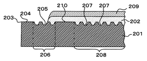
このような光情報記録媒体として、図3(A)〜図3(C)に示されるように、特許文献1には、基板101の一方の主面101a上に、例えば有機色素等からなる記録層103や透明な樹脂等からなる厚さ0.1mmのカバー層119等の複数の塗膜を厚み方向に重なるように形成する際、円環状の基板101の中心孔102を覆うキャップ104、114,124等を順次用いてスピンコート法により前記円環状の基板101の一方の主面101a側に順次塗布形成することが提案されている。 また、図4に示されるように、特許文献2には、円環状の基板201の一方の主面204の内周側に同心円状に溝205を設けることにより、塗膜202,209の内周側の縁部をほぼ真円状に形成することが提案されている。
上記特許文献1に記載の背景技術においては、前記円環状の基板101の一方の主面101a側に前記基板101の中心孔102の内径よりも大きな外径を有する第1のキャップ104を用い、該キャップの周縁部が前記基板の一方の主面101aの内周縁近傍と対向するように配置した状態で、ノズル108により例えば第1の塗布材料を前記キャップ104上に吐出し、前記円環状の基板101及び前記キャップ104を所定の回転プロファイルで回転させることにより、前記基板101の一方の主面101a側に下層の塗膜109が塗布形成される。このとき、前記基板101の表面と前記キャップ104の周縁部との隙間には毛細管現象により前記塗布液105が侵入するので、前記キャップ104を前記基板101の表面101aから引き離す際に塗膜109の内周縁近傍には表面に厚み方向の凹凸が生じやすい。次に、前記と同様に前記円環状の基板101の一方の主面101a側に形成された下層の塗膜109の上に該下層の塗膜109の内径よりも大きな外径を有する第2のキャップ114を用い、該キャップ114の周縁部が前記下層の塗膜109の内周縁近傍と対向するように配置した状態で、ノズル118により例えば第2の塗布材料115を前記第2のキャップ114上に吐出し、前記円環状の基板101及び前記第2のキャップ114を所定の回転プロファイルで回転させることにより、前記下層の塗膜109上に第2層の塗膜119が塗布形成される。
In the background art described in
ところがこのとき、上記下層の塗膜109の内周の近傍には前述のように厚み方向に凹凸が生じているので、前記第2のキャップ114の周縁部との隙間寸法にばらつきがあり、この隙間に毛細管現象により侵入する塗布液114の基板の中心方向への侵入度合いにばらつきを生じ、結果として前記上層の塗膜119の内周縁が周方向で蛇行を生じ、外観から粗製された商品であるかの如き印象を需要者に抱かせ、商品価値を低下させるという課題があった。また、前記下層の塗膜109の内周縁は前記上層の塗膜119の内周縁から中心側に部分的にはみ出して露出しているので、下層の塗膜109に空気中の湿気等が進入して光透過性の低下等の品質低下を生じる虞があった。
However, at this time, since the unevenness is generated in the thickness direction as described above in the vicinity of the inner periphery of the lower
本発明の目的は、上記課題を解決して、外観から粗製された商品であるかの如き印象を需要者に抱かせることのない光情報記録媒体を提供するものである。また、本発明は、上記課題を解決して、外観から粗製された商品であるかの如き印象を需要者に抱かせることのない光情報記録媒体の製造方法を提供するものである。 An object of the present invention is to provide an optical information recording medium that solves the above-described problems and does not give the consumer the impression that the product is a crude product from the appearance. The present invention also solves the above-described problems and provides a method for manufacturing an optical information recording medium that does not give a consumer the impression that the product is a crude product from the appearance.
前記目的を達成するため、本発明の光情報記録媒体は、(1)円環状の基板と該基板の一方の主面上に光反射層と光記録層と第1の光透過層と第2の光透過層とをこの順に有し、前記第2の光透過層側からレーザ光を照射することにより情報を記録及び/又は再生可能な光情報記録媒体において、前記基板の前記一方の主面の前記光記録層が設けられる領域より内周側に、第1の溝とさらに内周側の第2の溝とが同心円状に形成されており、前記第1の光透過層はその内周側の縁部が前記第1の溝の外周側の縁部近傍に位置するように設けられており、前記第2の光透過層はその内周側の縁部が前記第2の溝の外周側の縁部近傍に位置するように設けられている。(・・・以下、本発明の第1の課題解決手段と称する。) In order to achieve the above object, an optical information recording medium of the present invention comprises (1) an annular substrate, a light reflecting layer, an optical recording layer, a first light transmitting layer, and a second light on one main surface of the substrate. a of the light transmission layer in this order, in the second recording and / or renewable optical information recording medium information by irradiating a laser beam from the light transmitting layer side, wherein the one main surface of the substrate A first groove and a second groove on the inner peripheral side are formed concentrically on the inner peripheral side of the region where the optical recording layer is provided, and the first light transmission layer has an inner peripheral side thereof. And the second light transmission layer has an inner edge on the outer periphery of the second groove. It is provided so that it may be located in the edge part vicinity of the side. (... Hereinafter referred to as the first problem solving means of the present invention.)
また、本発明の光情報記録媒体の製造方法は、(2)円環状の基板の光反射層と光記録層とがこの順に形成された一方の主面上に、前記基板の中心孔を塞ぐ略円板状のキャップをそれぞれ用いて前記記録層を覆うようにスピンコート法により樹脂材料を塗布して第1及び第2の光透過層を順次形成する光情報記録媒体の製造方法において、一方の主面の内周側に同心円状に第1及び第2の溝が形成された円環状の基板を準備する工程と、該基板の前記主面上に光反射層を形成する工程と、該基板の前記光反射層上に光記録層を形成する工程と、第1のキャップをその周縁部が前記第1の溝の外周側の縁部近傍に対向するように配置してスピンコート法により透明樹脂材料を塗布して第1の光透過層を形成する工程と、前記第1のキャップより小径の第2のキャップをその周縁部が第2の溝の外周側の縁部近傍に対向するように配置してスピンコート法により透明樹脂材料を塗布して第2の光透過層を形成する工程と、を有する。(・・・以下、本発明の第2の課題解決手段と称する。) In the method for producing an optical information recording medium of the present invention, (2) the central hole of the substrate is closed on one main surface in which the light reflecting layer and the optical recording layer of the annular substrate are formed in this order. In the method for manufacturing an optical information recording medium, the first and second light transmission layers are sequentially formed by applying a resin material by spin coating so as to cover the recording layer using a substantially disc-shaped cap, respectively. Preparing an annular substrate having first and second grooves concentrically formed on the inner peripheral side of the main surface, forming a light reflecting layer on the main surface of the substrate, and A step of forming an optical recording layer on the light reflecting layer of the substrate, and a first cap is disposed by spin coating so that the peripheral portion thereof faces the vicinity of the outer peripheral portion of the first groove. A step of applying a transparent resin material to form a first light transmission layer, and the first cap A second cap having a diameter is arranged so that the peripheral edge thereof is opposed to the vicinity of the edge on the outer peripheral side of the second groove, and a transparent resin material is applied by spin coating to form a second light transmission layer. And a process. (... Hereinafter referred to as the second problem solving means of the present invention.)
上記第1の課題解決手段による作用は次の通りである。すなわち、前記基板の一方の主面の前記光記録層が設けられる領域より内周側に、第1の溝とさらに内周側の第2の溝とが同心円状に設けられており、前記第1の光透過層はその内周側の縁部が前記第1の溝の外周側の縁部近傍に位置するように設けられており、前記第2の光透過層はその内周側の縁部が前記第2の溝の外周側の縁部近傍に位置するように設けられているので、第2の光透過層の内周側が第1の光透過層の内周側の縁部を覆い前記第2の溝の外周側の縁部近傍に沿って形成されて、外観から粗製された商品であるかの如き印象を需要者に抱かせることを防止できる。 The operation of the first problem solving means is as follows. That is, the first groove and the second groove on the inner peripheral side are provided concentrically on the inner peripheral side of the region where the optical recording layer is provided on one main surface of the substrate, The first light transmission layer is provided so that the inner peripheral edge thereof is positioned in the vicinity of the outer peripheral edge of the first groove, and the second light transmission layer has an inner peripheral edge. Since the portion is provided in the vicinity of the outer peripheral edge of the second groove, the inner peripheral side of the second light transmission layer covers the inner peripheral edge of the first light transmission layer. It is formed along the vicinity of the outer peripheral edge of the second groove, and it is possible to prevent the consumer from giving an impression as if the product is a crude product from the appearance.
また、本発明の光情報記録媒体は、第2の光透過層の内周側が第1の光透過層の内周側の縁部を確実に被覆するので、前記第1の光透過層への空気中の湿気の進入等による光透過性の低下等の品質低下を生じる虞がないという効果も有する。 In the optical information recording medium of the present invention, the inner peripheral side of the second light transmission layer reliably covers the edge of the inner peripheral side of the first light transmission layer. There is also an effect that there is no risk of quality degradation such as a decrease in light transmission due to the ingress of moisture in the air.
また、上記第2の課題解決手段による作用は次の通りである。すなわち、一方の主面の内周側に同心円状に第1及び第2の溝が形成された円環状の基板を準備する工程と、該基板の前記主面上に光反射層を形成する工程と、該基板の前記光反射層上に光記録層を形成する工程と、第1のキャップをその周縁部が前記第1の溝の外周側の縁部近傍に対向するように配置してスピンコート法により透明樹脂材料を塗布して第1の光透過層を形成する工程と、前記第1のキャップより小径の第2のキャップをその周縁部が第2の溝の外周側の縁部近傍に対向するように配置してスピンコート法により透明樹脂材料を塗布して第2の光透過層を形成する工程と、を有するので、第2の光透過層を形成する際に基板の溝の外周側の縁部とキャップの外周縁近傍とを所定の間隔で対向させることができる。このため、多層の塗膜のうち、特に露出される上層の前記第2の光透過層の塗膜の内周側の縁部にそれぞれ周方向で毛細管現象の発生ばらつきによる蛇行が生じるのを抑制することができ、外観から粗製された商品であるかの如き印象を需要者に抱かせることを防止できる。 The operation of the second problem solving means is as follows. That is, a step of preparing an annular substrate having first and second grooves formed concentrically on the inner peripheral side of one main surface, and a step of forming a light reflecting layer on the main surface of the substrate And a step of forming an optical recording layer on the light reflecting layer of the substrate, and a first cap is disposed so that a peripheral portion thereof faces an outer peripheral portion of the first groove. A step of forming a first light transmission layer by applying a transparent resin material by a coating method; and a peripheral portion of a second cap having a smaller diameter than the first cap, in the vicinity of the peripheral portion of the second groove And a step of forming a second light transmission layer by applying a transparent resin material by a spin coating method so as to face the substrate, so that the groove of the substrate is formed when the second light transmission layer is formed. The peripheral edge and the vicinity of the outer peripheral edge of the cap can be opposed to each other at a predetermined interval. For this reason, it is possible to suppress meandering due to variation in the occurrence of capillarity in the circumferential direction at the inner peripheral edge of the coating film of the second light transmission layer, which is the upper layer, among the multilayer coating film. It is possible to prevent the consumer from giving the impression that the product is a crude product from the appearance.
本発明の光情報記録媒体によれば、外観から粗製された商品であるかの如き印象を需要者に抱かせることを防止でき、商品価値の低下のない光情報記録媒体を提供することができる。また、本発明によれば、外観から粗製された商品であるかの如き印象を需要者に抱かせることを防止でき、商品価値の低下のない光情報記録媒体の製造方法を提供することができる。本発明の前記目的とそれ以外の目的、構成特徴、作用効果は、以下の説明と添付図面によって明らかとなろう。 According to the optical information recording medium of the present invention, it is possible to prevent the consumer from having an impression as if it is a crude product from the appearance, and it is possible to provide an optical information recording medium that does not cause a decrease in commercial value. . In addition, according to the present invention, it is possible to prevent a consumer from having an impression as if it is a product that is crude from the appearance, and to provide a method for manufacturing an optical information recording medium that does not cause a reduction in product value. . The above object and other objects, structural features, and operational effects of the present invention will become apparent from the following description and the accompanying drawings.
以下、本発明の光情報記録媒体の第1の実施形態について、図1を参照して説明する。図1は第1の実施形態の光情報記録媒体10の内部構造の要部を示す部分拡大断面図である。尚、同図は円環状の基板11の中心から右側の要部のみを示したものであり、左側については基板の中心線に対し右側とほぼ対称であるため記載を省略した。
Hereinafter, a first embodiment of the optical information recording medium of the present invention will be described with reference to FIG. FIG. 1 is a partial enlarged cross-sectional view showing the main part of the internal structure of the optical
図1に示すように、本実施形態の光情報記録媒体10は、円環状の基板11の一方の主面11a上に光反射層13と光記録層15と樹脂塗膜からなる第1の光透過層17及び第2の光透過層18とをこの順に有するものである。
As shown in FIG. 1, the optical
具体的には、円環状の基板11と該基板11の一方の主面11a上に光反射層13と光記録層15と保護層16と第1の光透過層17と第2の光透過層18とをこの順に有し、前記第2の光透過層18側からレーザ光を照射することにより情報を記録及び/又は再生可能な光情報記録媒体10であって、前記円環状の基板11の一方の主面11aには、通常直径46mm〜直径117mmの範囲に、レーザ光照射による記録及び/又は再生のトラッキングガイド用の螺旋状溝11bが形成されるとともに、該螺旋状溝11bを覆うように光反射層13が形成されている。そして、該光反射層13の上に光記録層15が形成されている。前記基板11の一方の主面11a側の前記光記録層15が設けられる領域より内周側に、第1の溝11c1とさらに内周側の第2の溝11c2とが同心円状に形成されており、前記第1の光透過層17はその内周側の縁部17eが前記第1の溝11c1の外周側の縁部e1近傍に位置するように設けられている。そして、前記第2の光透過層18はその内周側の縁部18eが前記第2の溝11c2の外周側の縁部e2近傍に位置するように設けられている。
Specifically, an
次に、上記基板11の好ましい実施形態は次の通りである。すなわち、上記基板11としては、従来の光情報記録媒体の基板材料として用いられている各種の材料を任意に選択して使用することができる。具体的には、ポリカーボネート、ポリメチルメタクリレート等のアクリル樹脂、ポリ塩化ビニル、塩化ビニル共重合体等の塩化ビニル系樹脂、エポキシ樹脂、アモルファスポリオレフィン、ポリエステル樹脂、アルミニウム等の金属、ガラス等を挙げることができ、必要によりこれらを積層して併用してもよい。上記材料の中では、成型性、耐湿性、寸法安定性及び低価格等の点から熱可塑性樹脂が好ましく、ポリカーボネートが特に好ましい。
これらの樹脂を用いた場合には、射出成形等の方法で所定の形状(光ディスクなら円環状)に基板11を作成することが好ましい。また、上記基板11の厚さは0.9〜1.6mmの範囲とすることが好ましい。また、これに限るものではなく、例えば紫外線硬化性樹脂を用いて、基台上に塗布し塗膜を硬化させて用いることもできる。
Next, a preferred embodiment of the
When these resins are used, it is preferable to form the
上記基板11には、光反射層13が設けられる一方の主面11aに、レーザ光照射による記録及び/又は再生のトラッキングガイド用の螺旋状溝11bが形成されていることが好ましい。該螺旋状溝11bは、深さ20nm〜300nm,ピッチは、通常500nm以下であることが好ましい。また、前記螺旋状溝11bは、図示省略するが、前記基板11の成型に用いられる金型内に、一方の主面に前記螺旋状溝11bとは逆パターンの高さ20nm〜300nmの螺旋状の凸条の微細加工が施されたスタンパと呼ばれる型板を配置して前記基板11の射出成型時に同時に形成することが好ましい。
The
次に、上記同心円状の第1の溝11c1及び第2の溝11c2の好ましい実施形態は次の通りである。すなわち、上記同心円状の第1の溝11c1及び第2の溝11c2としては、上記基板11の前記光記録層15が設けられる側の面に、前記螺旋状溝11bが形成される領域より内周寄りに前記基板11の成型と同時に形成されることが好ましい。前記第1の溝11c1及び第2の溝11c2の深さは0.02mm〜1.0mmが好ましい。また、前記第1の溝11c1及び第2の溝11c2の幅は0.02mm〜1.0mmが好ましい。また、前記第1の溝11c1及び第2の溝11c2のピッチは0.02mm〜1.0mmが好ましい。上記第1の溝11c1及び第2の溝11c2は、前記基板11の中心線を中心に環状に形成されることが好ましい。
前記同心円状の第1の溝11c1及び第2の溝11c2は、前記トラッキングガイド用の螺旋状溝11bに比べて深さが深く、前記スタンパにより形成することが難しい。このため、図示省略するが、前記基板11の成型用の金型の内面に直接、もしくは前記金型の内部に前記スタンパの内周側を固定するためのセンターホルダの表面に、前記同心円状の溝11cとは逆パターンの同心円状の複数の凸条を設けることにより、前記基板11の成型と同時に形成することが好ましい。
Next, a preferred embodiment of the concentric first groove 11c1 and second groove 11c2 is as follows. In other words, the concentric first groove 11c1 and the second groove 11c2 are formed on the inner surface of the
The concentric first groove 11c1 and the second groove 11c2 are deeper than the tracking
次に、上記光反射層13の好ましい実施形態は次のとおりである。上記光反射層13はデータの記録および/または再生用のレーザ光を反射させるものであり、本発明においては、レーザ光に対する反射率を高めたり、記録再生特性を改良する機能を付与するために、基板11と色素層15との間に、必要により設けることが好ましい。上記光反射層13としては、Au,Al,Ag,CuあるいはPd等の金属膜、これらの金属の合金膜あるいはこれらの金属に微量成分が添加された合金膜等が好ましく、例えば蒸着法、イオンプレーティング法、スパッタリング法、等により前記基板11のプリグルーブ11bが形成された面11a上に形成されることが好ましい。中でも、量産性、コストの面からスパッタリング法が特に好ましい。
Next, a preferred embodiment of the
次に、上記光記録層15の好ましい実施形態は次の通りである。すなわち、上記光記録層15としては、有機色素を記録物質として含有する色素型とすることが好ましい。中でも、レーザ光照射によりピットが形成されデータが記録される色素型の記録層であることが好ましい。上記有機色素としては、フタロシアニン色素、シアニン色素、アゾ系色素等が好ましい。上記色素層15には、上記レーザ光の照射により音楽や画像、コンピュータプログラム等のデータ情報を記録及び/又は再生することができる。また、上記色素層15は、上記色素を結合剤等と共に適当な溶剤に溶解して塗布液を調整し、次いで、この塗布液を、基板11上に直接または他の層を介してスピンコート法やスクリーン印刷法等により塗布して塗膜を形成した後、乾燥することにより形成される。尚、前記他の層としては、前述の光反射層13等がある。
Next, a preferred embodiment of the
次に、上記保護層16の好ましい実施形態は次の通りである。すなわち、上記保護層16としては、ZnS、SiO2,SiN,AlN,ZnS−SiO2,SiC等の材料を使用し、蒸着、スパッタ等の手段により形成することが好ましい。上記保護層16は、上記色素層15と上記カバー層17の間に、記録特性等の調整や接着性向上あるいは記録層の保護等を目的として必要により形成されることが好ましい。
Next, a preferred embodiment of the
次に、上記第1の光透過層17の好ましい実施形態は次の通りである。すなわち、上記第1の光透過層17としては、透明な紫外線硬化性樹脂を適当な溶剤に溶解して塗布液を調整し、次いで、第1のキャップを用い、この塗布液を上記光記録層15を覆うようにスピンコート法により塗布して塗膜を形成した後、乾燥し、紫外線を照射することにより形成される。
Next, a preferred embodiment of the first
次に、上記第2の光透過層18の好ましい実施形態は次の通りである。すなわち、上記第2の光透過層18としては、透明な紫外線硬化性樹脂を適当な溶剤に溶解して塗布液を調整し、次いで、前記第1のキャップより小径の第2のキャップを用い、この塗布液を上記第1の光透過層17を覆うようにスピンコート法により塗布して塗膜を形成した後、乾燥し、紫外線を照射することにより形成される。
Next, a preferred embodiment of the second
上記第1の光透過層17及び第2の光透過層18の合計厚みは通常400nm〜500nm付近の波長のレーザ光が照射されて前記記録層にデータ記録/及びまたは前記記録層から再生されるように構成されるために、通常0.1mmであることが好ましい。
尚、上記光記録層15と上記第1の光透過層17との間に、記録特性等の調整や接着性向上あるいは光記録層の保護等を目的として、前述したように保護層16を形成することが好ましく、この場合には、それらの層と光記録層15、第1の光透過層17及び第2の光透過層18を合わせた厚さが0.1mm程度であることが好ましい。
The total thickness of the first light-transmitting
The
次に、本発明の光情報記録媒体の製造方法の第1の実施形態について、図2を参照して説明する。図2は第1の実施形態の光情報記録媒体10の製造方法を各ステップを追って説明するための部分拡大断面図である。尚、同図は円環状の基板11の中心から右側の要部のみを示したものであり、左側については右側と対称であるため記載を省略した。
Next, a first embodiment of the method for producing an optical information recording medium of the present invention will be described with reference to FIG. FIG. 2 is a partial enlarged cross-sectional view for explaining the manufacturing method of the optical
本実施形態の光情報記録媒体10の製造方法は、図1に示すように、円環状の基板11の光反射層13と光記録層15とがこの順に形成された一方の主面11a上に、前記基板11の中心孔12を塞ぐ略円板状のキャップ14をそれぞれ用いて前記光記録層15を覆うようにスピンコート法により透明樹脂材料の塗布液を塗布して第1及び第2の光透過層を順次形成する光情報記録媒体10の製造方法であって、一方の主面の内周側に同心円状に第1の溝11c1及び第2の溝11c2が形成された円環状の基板11を準備する工程と、図2(A)に示すように該基板11の前記主面11a上に光反射層13を形成する工程と、図2(B)及び図2(C)に示すように該基板11の前記光反射層13上に光記録層15を形成する工程と、図2(E)に示すように第1のキャップ14a1をその周縁部14a1eが前記第1の溝11c1の外周側の縁部e1近傍に対向するように配置し、図2(F)に示すように、透明樹脂材料の塗布液17aをスピンコート法により塗布して図2(G)に示すように第1の光透過層17を形成する工程と、図2(H)に示すように、前記第1のキャップ14a1より小径の第2のキャップ14a2をその周縁部14a2eが前記第1の溝11c1より内周寄りの第2の溝11c2の外周側の縁部e2近傍に対向するように配置し、図2(I)に示すように、透明樹脂材料の塗布液18aをスピンコート法により塗布して図2(J)に示すように第2の光透過層18を形成する工程と、を有するものである。
As shown in FIG. 1, the manufacturing method of the optical
(実施例1)まず、厚さ1.1mm、外形120mm、中心孔12の内径15mmの円環状で一方の主面11a側に、トラックピッチ0.32μmでスパイラル状の螺旋状溝11bと、基板中心からの径が22mm〜44mmの領域にピッチ0.4mm,溝幅0.2mm,溝深さ0.1mmで同心円状の第1の溝11c1及び第2の溝11c2と、前記第1の溝11c1と前記螺旋状溝11bとの間に予備の溝11c0と、を有する、ポリカーボネート樹脂からなる基板11を射出成形法により成形した。(図示省略)
(Embodiment 1) First, a
次に、図2(A)に示すように、前記基板11の螺旋状溝11bが形成された一方の主面11a側に前記螺旋状溝11bを覆うように,スパッタリングにより厚さ100nmのAg合金からなる光反射層13を形成した。
Next, as shown in FIG. 2A, an Ag alloy having a thickness of 100 nm is formed by sputtering so as to cover the
次に、有機色素の塗布液15aを準備し、上記基板11の前記一方の主面11a側に、図2(B)に示すように、ノズル14b1から前記塗布液15aを滴下し、図2(C)に示すようにスピンコート法により所定の回転プロファイルで前記基板を回転させて遠心力により前記光反射層13を覆うように光記録層15を形成した。
Next, an organic pigment coating solution 15a is prepared, and the coating solution 15a is dropped from the nozzle 14b1 onto the one
次に、図2(D)に示すように、上記基板11の前記一方の主面11a側に内周側の縁部が前記予備溝11c0の外周側の縁部e0近傍に位置し前記光記録層15を覆うようにスパッタリングにより厚さ50nmのSiO2からなる保護層16を形成した。
Next, as shown in FIG. 2D, an edge on the inner peripheral side of the
次に、図2(E)に示すように、上記基板11の前記一方の主面11a側に第1のキャップ14a1をその周縁部14a1eが前記第1の溝11c1の外周側の縁部e1近傍に対向するように配置し、図2(F)に示すように、ノズル14b2から紫外線硬化性の透明樹脂材料の塗布液17aを前記第1のキャップ14a1を介してスピンコート法により塗布して図2(G)に示すように前記保護層16を覆う厚さ20μmの第1の光透過層17を形成した。
Next, as shown in FIG. 2E, the first cap 14a1 is placed on the one
次に、図2(H)に示すように、前記第1のキャップ14a1より小径の第2のキャップ14a2をその周縁部14a2eが前記第1の溝11c1より内周寄りの第2の溝11c2の外周側の縁部e2近傍に対向するように配置した。そして、図2(I)に示すように、ノズル14b3から紫外線硬化性の透明樹脂材料の塗布液18aを前記第2のキャップ14a2を介してスピンコート法により塗布して図2(J)に示すように前記第1の光透過層17を覆う厚さ80μmの第2の光透過層18を形成した。これらの工程により、実施例1の光情報記録媒体10が作成された。
Next, as shown in FIG. 2 (H), the second cap 14a2 having a smaller diameter than the first cap 14a1 is formed in the second groove 11c2 whose peripheral edge portion 14a2e is closer to the inner periphery than the first groove 11c1. It arrange | positioned so that the edge part e2 vicinity of an outer peripheral side might be opposed. Then, as shown in FIG. 2 (I), a coating liquid 18a of an ultraviolet curable transparent resin material is applied from the nozzle 14b3 through the second cap 14a2 by a spin coating method, and shown in FIG. 2 (J). Thus, a second
上記で得られた光情報記録媒体10の前記一方の主面11a側の前記第1の溝11c1上の前記第1の光透過層17の内周側の縁部17e,前記第2の溝11c2上の前記第2の光透過層18の内周側の縁部18eをそれぞれ光学顕微鏡により10倍に拡大して観察した結果、毛細管現象の発生ばらつきによる周方向での蛇行は見当たらなかった。また、前記第1の光透過層17は内周側の縁部17eまで完全に前記第2の光透過層18に被覆されており、縁部の露出は見当たらず、品質低下が生じる虞がないものであることが確認された。
The
(比較例1)また、第1のキャップの代わりに第2のキャップを用いて第1の光透過層を形成したこと以外は前記実施例1と同様にして比較例の光情報記録媒体を作成し、前記実施例と同様に光情報記録媒体の前記一方の主面側の第1の光透過層の縁部、第2の光透過層の縁部をそれぞれ光学顕微鏡により10倍に拡大して観察した結果、前記第1の光透過層の縁部及び第2の光透過層の縁部にそれぞれ毛細管現象の発生ばらつきによる周方向での蛇行が観察された。また、前記第1の光透過層は内周側の縁部が前記第2の光透過層から露出されており、品質低下が生じる虞があることが確認された。 (Comparative Example 1) An optical information recording medium of a comparative example was prepared in the same manner as in Example 1 except that the first light transmitting layer was formed using the second cap instead of the first cap. In the same manner as in the above embodiment, the edge of the first light transmission layer and the edge of the second light transmission layer on the one main surface side of the optical information recording medium are each magnified 10 times by an optical microscope. As a result of observation, meandering in the circumferential direction due to occurrence of capillary action was observed at the edge of the first light transmission layer and the edge of the second light transmission layer, respectively. Moreover, it was confirmed that the edge part of the inner peripheral side of the first light transmission layer is exposed from the second light transmission layer, and there is a possibility that the quality deteriorates.
上記実施例では、保護層16を設けたが、本発明はこれに限定するものではなく、保護層16を省略してもよい。また、上記実施例では、基板11の一方の主面11a側の前記第1の溝11c1と前記螺旋状溝11bとの間に予備溝11c0を設けたが、本発明はこれに限定するものではなく、予備溝11c0を省略してもよい。また、前記第1の溝11c1と前記第2の溝11c2との間や、前記第2の溝11c2よりさらに内周側に前記と同様に予備溝を設けてもよい。
In the above embodiment, the
10:光情報記録媒体11:基板11a:一方の主面11b:螺旋状溝11c:同心円状の溝11c0:予備溝11c1:第1の溝11c2:第2の溝 12:中心孔13:光反射層14a1:第1のキャップ14a1e:周縁部14a2:第2のキャップ14a2e:周縁部14b1:ノズル14b2:ノズル14b3:ノズル15:光記録層15e:内周側の縁部16:保護層16e:内周側の縁部17:第1の光透過層17e:内周側の縁部18:第2の光透過層18e:内周側の縁部e0:予備溝の外周側の縁部e1:第1の溝の外周側の縁部e2:第2の溝の外周側の縁部
10: Optical information recording medium 11:
Claims (2)
Priority Applications (5)
| Application Number | Priority Date | Filing Date | Title |
|---|---|---|---|
| JP2007055099A JP4714703B2 (en) | 2007-03-06 | 2007-03-06 | Optical information recording medium manufacturing method and optical information recording medium |
| US12/035,981 US20080248254A1 (en) | 2007-03-06 | 2008-02-22 | Method of manufacturing optical information recording medium and the optical information recording medium |
| TW097106860A TW200842865A (en) | 2007-03-06 | 2008-02-27 | Method of manufacturing optical information recording medium and the optical information recording medium |
| CN200810008026.5A CN101261853B (en) | 2007-03-06 | 2008-03-03 | Optical information recording medium and manufacturing method thereof |
| HK08113313.5A HK1119827A1 (en) | 2007-03-06 | 2008-12-08 | An optical information recording medium and method for producing the same |
Applications Claiming Priority (1)
| Application Number | Priority Date | Filing Date | Title |
|---|---|---|---|
| JP2007055099A JP4714703B2 (en) | 2007-03-06 | 2007-03-06 | Optical information recording medium manufacturing method and optical information recording medium |
Publications (3)
| Publication Number | Publication Date |
|---|---|
| JP2008217915A JP2008217915A (en) | 2008-09-18 |
| JP2008217915A5 JP2008217915A5 (en) | 2010-04-22 |
| JP4714703B2 true JP4714703B2 (en) | 2011-06-29 |
Family
ID=39827193
Family Applications (1)
| Application Number | Title | Priority Date | Filing Date |
|---|---|---|---|
| JP2007055099A Expired - Fee Related JP4714703B2 (en) | 2007-03-06 | 2007-03-06 | Optical information recording medium manufacturing method and optical information recording medium |
Country Status (5)
| Country | Link |
|---|---|
| US (1) | US20080248254A1 (en) |
| JP (1) | JP4714703B2 (en) |
| CN (1) | CN101261853B (en) |
| HK (1) | HK1119827A1 (en) |
| TW (1) | TW200842865A (en) |
Families Citing this family (2)
| Publication number | Priority date | Publication date | Assignee | Title |
|---|---|---|---|---|
| US8119216B2 (en) * | 2007-12-12 | 2012-02-21 | Taiyo Yuden Co., Ltd. | Optical information recording medium and manufacturing method thereof |
| US8529991B2 (en) * | 2009-07-31 | 2013-09-10 | Raytheon Canada Limited | Method and apparatus for cutting a part without damaging a coating thereon |
Citations (2)
| Publication number | Priority date | Publication date | Assignee | Title |
|---|---|---|---|---|
| JP2001256683A (en) * | 2000-03-14 | 2001-09-21 | Hitachi Ltd | Device for producing information recording medium, method therefor and the information recording medium |
| JP2004022074A (en) * | 2002-06-17 | 2004-01-22 | Sharp Corp | Recording medium, apparatus for manufacturing the same, and recording medium manufacturing method |
Family Cites Families (3)
| Publication number | Priority date | Publication date | Assignee | Title |
|---|---|---|---|---|
| US6700862B2 (en) * | 2000-10-03 | 2004-03-02 | Matsushita Electric Industrial Co., Ltd. | Optical disc and manufacturing method for the same |
| JP2003067990A (en) * | 2001-08-29 | 2003-03-07 | Tdk Corp | Forming method of information recording layer on optical recording medium, and manufacturing method of optical recording medium |
| CN100397516C (en) * | 2004-11-22 | 2008-06-25 | 日本胜利株式会社 | Optical disk and method of producing the same |
-
2007
- 2007-03-06 JP JP2007055099A patent/JP4714703B2/en not_active Expired - Fee Related
-
2008
- 2008-02-22 US US12/035,981 patent/US20080248254A1/en not_active Abandoned
- 2008-02-27 TW TW097106860A patent/TW200842865A/en unknown
- 2008-03-03 CN CN200810008026.5A patent/CN101261853B/en not_active Expired - Fee Related
- 2008-12-08 HK HK08113313.5A patent/HK1119827A1/en not_active IP Right Cessation
Patent Citations (2)
| Publication number | Priority date | Publication date | Assignee | Title |
|---|---|---|---|---|
| JP2001256683A (en) * | 2000-03-14 | 2001-09-21 | Hitachi Ltd | Device for producing information recording medium, method therefor and the information recording medium |
| JP2004022074A (en) * | 2002-06-17 | 2004-01-22 | Sharp Corp | Recording medium, apparatus for manufacturing the same, and recording medium manufacturing method |
Also Published As
| Publication number | Publication date |
|---|---|
| CN101261853A (en) | 2008-09-10 |
| JP2008217915A (en) | 2008-09-18 |
| HK1119827A1 (en) | 2009-03-13 |
| TW200842865A (en) | 2008-11-01 |
| CN101261853B (en) | 2010-08-11 |
| US20080248254A1 (en) | 2008-10-09 |
Similar Documents
| Publication | Publication Date | Title |
|---|---|---|
| JP5094698B2 (en) | Dye for optical information recording medium and optical information recording medium | |
| JP4714703B2 (en) | Optical information recording medium manufacturing method and optical information recording medium | |
| US8305852B2 (en) | Optical information recording medium | |
| TWI386935B (en) | Optical information recording media | |
| JP2007294055A (en) | Optical information recording medium and method for manufacturing the same | |
| US20060023620A1 (en) | Optical information recording medium | |
| JP4708316B2 (en) | Optical information recording medium | |
| JP4588081B2 (en) | Optical information recording medium and manufacturing method thereof | |
| JP2009006615A (en) | Optical disk and mold assembly | |
| JP5408851B2 (en) | Optical information recording medium | |
| JP2003217171A (en) | Optical recording medium and manufacturing method therefor | |
| JP2005310320A (en) | Optical information recording medium | |
| JP4714666B2 (en) | Optical information recording medium | |
| JP2008186509A (en) | Optical information recording medium and its manufacturing method | |
| JP2008004174A (en) | Metal mold for optical information recording medium and optical information recording medium | |
| JP2007035081A (en) | Optical information recording medium | |
| JP2008010025A (en) | Manufacturing method of optical information recording medium, and optical information recording medium | |
| JP2007109353A (en) | Optical information recording medium | |
| JP2003157587A (en) | Disk for testing reproduction | |
| JP2006018980A (en) | Optical disk and its manufacturing method | |
| US20090180374A1 (en) | Optical information recording medium and method for producing the same | |
| JPH03120636A (en) | Information recording medium and its production | |
| US20050073942A1 (en) | Optical recording medium and method of manufacturing the same | |
| JP2004355751A (en) | Optical recording medium | |
| JP2009163858A (en) | Optical information recording media and method for producing the same |
Legal Events
| Date | Code | Title | Description |
|---|---|---|---|
| A521 | Request for written amendment filed |
Free format text: JAPANESE INTERMEDIATE CODE: A523 Effective date: 20100304 |
|
| A621 | Written request for application examination |
Free format text: JAPANESE INTERMEDIATE CODE: A621 Effective date: 20100304 |
|
| A977 | Report on retrieval |
Free format text: JAPANESE INTERMEDIATE CODE: A971007 Effective date: 20110228 |
|
| A01 | Written decision to grant a patent or to grant a registration (utility model) |
Free format text: JAPANESE INTERMEDIATE CODE: A01 Effective date: 20110303 |
|
| A61 | First payment of annual fees (during grant procedure) |
Free format text: JAPANESE INTERMEDIATE CODE: A61 Effective date: 20110328 |
|
| R250 | Receipt of annual fees |
Free format text: JAPANESE INTERMEDIATE CODE: R250 |
|
| R250 | Receipt of annual fees |
Free format text: JAPANESE INTERMEDIATE CODE: R250 |
|
| R250 | Receipt of annual fees |
Free format text: JAPANESE INTERMEDIATE CODE: R250 |
|
| LAPS | Cancellation because of no payment of annual fees |