JP2008031555A5 - - Google Patents
Download PDFInfo
- Publication number
- JP2008031555A5 JP2008031555A5 JP2007175071A JP2007175071A JP2008031555A5 JP 2008031555 A5 JP2008031555 A5 JP 2008031555A5 JP 2007175071 A JP2007175071 A JP 2007175071A JP 2007175071 A JP2007175071 A JP 2007175071A JP 2008031555 A5 JP2008031555 A5 JP 2008031555A5
- Authority
- JP
- Japan
- Prior art keywords
- resin
- plating
- sputtering
- molded product
- resin molded
- Prior art date
- Legal status (The legal status is an assumption and is not a legal conclusion. Google has not performed a legal analysis and makes no representation as to the accuracy of the status listed.)
- Granted
Links
- 229920005989 resin Polymers 0.000 claims description 258
- 239000011347 resin Substances 0.000 claims description 258
- 238000007747 plating Methods 0.000 claims description 153
- 229910052751 metal Inorganic materials 0.000 claims description 108
- 239000002184 metal Substances 0.000 claims description 108
- 239000010408 film Substances 0.000 claims description 100
- 238000004544 sputter deposition Methods 0.000 claims description 96
- PXHVJJICTQNCMI-UHFFFAOYSA-N nickel Chemical compound [Ni] PXHVJJICTQNCMI-UHFFFAOYSA-N 0.000 claims description 66
- 238000000034 method Methods 0.000 claims description 58
- 239000010409 thin film Substances 0.000 claims description 41
- 238000009713 electroplating Methods 0.000 claims description 39
- 238000004519 manufacturing process Methods 0.000 claims description 31
- 238000004140 cleaning Methods 0.000 claims description 30
- 230000004913 activation Effects 0.000 claims description 29
- 229910052759 nickel Inorganic materials 0.000 claims description 29
- 239000011651 chromium Substances 0.000 claims description 25
- 238000009832 plasma treatment Methods 0.000 claims description 25
- XKRFYHLGVUSROY-UHFFFAOYSA-N argon Chemical compound [Ar] XKRFYHLGVUSROY-UHFFFAOYSA-N 0.000 claims description 18
- VYZAMTAEIAYCRO-UHFFFAOYSA-N chromium Chemical compound [Cr] VYZAMTAEIAYCRO-UHFFFAOYSA-N 0.000 claims description 17
- 229910052804 chromium Inorganic materials 0.000 claims description 17
- 239000010949 copper Substances 0.000 claims description 17
- 239000012298 atmosphere Substances 0.000 claims description 16
- 230000015572 biosynthetic process Effects 0.000 claims description 16
- 238000005755 formation reaction Methods 0.000 claims description 16
- 239000001301 oxygen Substances 0.000 claims description 15
- MYMOFIZGZYHOMD-UHFFFAOYSA-N oxygen Chemical compound O=O MYMOFIZGZYHOMD-UHFFFAOYSA-N 0.000 claims description 15
- 229910052760 oxygen Inorganic materials 0.000 claims description 15
- RYGMFSIKBFXOCR-UHFFFAOYSA-N copper Chemical compound [Cu] RYGMFSIKBFXOCR-UHFFFAOYSA-N 0.000 claims description 13
- 229910052802 copper Inorganic materials 0.000 claims description 13
- 230000004048 modification Effects 0.000 claims description 12
- 238000006011 modification reaction Methods 0.000 claims description 12
- 229910045601 alloy Inorganic materials 0.000 claims description 9
- 239000000956 alloy Substances 0.000 claims description 9
- 229910052786 argon Inorganic materials 0.000 claims description 9
- REDXJYDRNCIFBQ-UHFFFAOYSA-N aluminium(3+) Chemical class [Al+3] REDXJYDRNCIFBQ-UHFFFAOYSA-N 0.000 claims description 8
- 238000001994 activation Methods 0.000 claims description 7
- ARUVKPQLZAKDPS-UHFFFAOYSA-L Copper(II) sulfate Chemical compound [Cu+2].[O-][S+2]([O-])([O-])[O-] ARUVKPQLZAKDPS-UHFFFAOYSA-L 0.000 claims description 6
- 229910000365 copper sulfate Inorganic materials 0.000 claims description 6
- 229910000990 Ni alloy Inorganic materials 0.000 claims description 5
- 239000005092 Ruthenium Substances 0.000 claims description 3
- 229910001128 Sn alloy Inorganic materials 0.000 claims description 3
- 230000003213 activating Effects 0.000 claims description 3
- PCHJSUWPFVWCPO-UHFFFAOYSA-N gold Chemical compound [Au] PCHJSUWPFVWCPO-UHFFFAOYSA-N 0.000 claims description 3
- 229910052737 gold Inorganic materials 0.000 claims description 3
- 239000010931 gold Substances 0.000 claims description 3
- KJTLSVCANCCWHF-UHFFFAOYSA-N ruthenium Chemical compound [Ru] KJTLSVCANCCWHF-UHFFFAOYSA-N 0.000 claims description 3
- 229910052707 ruthenium Inorganic materials 0.000 claims description 3
- 239000004020 conductor Substances 0.000 claims 1
- 238000002425 crystallisation Methods 0.000 claims 1
- 230000005712 crystallization Effects 0.000 claims 1
- 239000007789 gas Substances 0.000 claims 1
- 239000004417 polycarbonate Substances 0.000 description 25
- KRVSOGSZCMJSLX-UHFFFAOYSA-L Chromic acid Chemical compound O[Cr](O)(=O)=O KRVSOGSZCMJSLX-UHFFFAOYSA-L 0.000 description 24
- 238000005530 etching Methods 0.000 description 23
- 239000000463 material Substances 0.000 description 23
- QAOWNCQODCNURD-UHFFFAOYSA-N Sulfuric acid Chemical compound OS(O)(=O)=O QAOWNCQODCNURD-UHFFFAOYSA-N 0.000 description 18
- 238000005259 measurement Methods 0.000 description 13
- 229920000122 Acrylonitrile butadiene styrene Polymers 0.000 description 12
- 210000002381 Plasma Anatomy 0.000 description 12
- 239000000126 substance Substances 0.000 description 11
- 229920000139 polyethylene terephthalate Polymers 0.000 description 10
- 239000005020 polyethylene terephthalate Substances 0.000 description 10
- 239000002253 acid Substances 0.000 description 9
- 238000007772 electroless plating Methods 0.000 description 9
- 239000002994 raw material Substances 0.000 description 9
- 238000000465 moulding Methods 0.000 description 8
- PPBRXRYQALVLMV-UHFFFAOYSA-N styrene Chemical compound C=CC1=CC=CC=C1 PPBRXRYQALVLMV-UHFFFAOYSA-N 0.000 description 8
- 229910018487 Ni—Cr Inorganic materials 0.000 description 7
- 239000011248 coating agent Substances 0.000 description 7
- 238000000576 coating method Methods 0.000 description 7
- 238000010586 diagram Methods 0.000 description 7
- VEXZGXHMUGYJMC-UHFFFAOYSA-N HCl Chemical compound Cl VEXZGXHMUGYJMC-UHFFFAOYSA-N 0.000 description 6
- JOPOVCBBYLSVDA-UHFFFAOYSA-N chromium(6+) Chemical compound [Cr+6] JOPOVCBBYLSVDA-UHFFFAOYSA-N 0.000 description 6
- 239000010410 layer Substances 0.000 description 6
- 238000001755 magnetron sputter deposition Methods 0.000 description 6
- XLYOFNOQVPJJNP-UHFFFAOYSA-N water Substances O XLYOFNOQVPJJNP-UHFFFAOYSA-N 0.000 description 6
- 239000000853 adhesive Substances 0.000 description 5
- 230000001070 adhesive Effects 0.000 description 5
- 229920001707 polybutylene terephthalate Polymers 0.000 description 5
- -1 polyethylene terephthalate Polymers 0.000 description 5
- 238000002203 pretreatment Methods 0.000 description 5
- 239000000243 solution Substances 0.000 description 5
- 238000005406 washing Methods 0.000 description 5
- 239000004677 Nylon Substances 0.000 description 4
- 239000004734 Polyphenylene sulfide Substances 0.000 description 4
- NLHHRLWOUZZQLW-UHFFFAOYSA-N acrylonitrile Chemical compound C=CC#N NLHHRLWOUZZQLW-UHFFFAOYSA-N 0.000 description 4
- KAKZBPTYRLMSJV-UHFFFAOYSA-N butadiene Chemical compound C=CC=C KAKZBPTYRLMSJV-UHFFFAOYSA-N 0.000 description 4
- 238000000151 deposition Methods 0.000 description 4
- 230000000694 effects Effects 0.000 description 4
- 150000002739 metals Chemical class 0.000 description 4
- 229920001778 nylon Polymers 0.000 description 4
- 238000010422 painting Methods 0.000 description 4
- 230000002093 peripheral Effects 0.000 description 4
- 229920000069 poly(p-phenylene sulfide) Polymers 0.000 description 4
- 229920000515 polycarbonate Polymers 0.000 description 4
- 239000004977 Liquid-crystal polymers (LCPs) Substances 0.000 description 3
- 239000004952 Polyamide Substances 0.000 description 3
- 239000004743 Polypropylene Substances 0.000 description 3
- 239000004793 Polystyrene Substances 0.000 description 3
- 125000004429 atoms Chemical group 0.000 description 3
- 238000005260 corrosion Methods 0.000 description 3
- 238000001035 drying Methods 0.000 description 3
- 239000000428 dust Substances 0.000 description 3
- 238000002347 injection Methods 0.000 description 3
- 239000007924 injection Substances 0.000 description 3
- 239000011810 insulating material Substances 0.000 description 3
- 150000002500 ions Chemical class 0.000 description 3
- KDLHZDBZIXYQEI-UHFFFAOYSA-N palladium Substances [Pd] KDLHZDBZIXYQEI-UHFFFAOYSA-N 0.000 description 3
- 229920002647 polyamide Polymers 0.000 description 3
- 239000011528 polyamide (building material) Substances 0.000 description 3
- 229920001955 polyphenylene ether Polymers 0.000 description 3
- KWYUFKZDYYNOTN-UHFFFAOYSA-M potassium hydroxide Chemical compound [OH-].[K+] KWYUFKZDYYNOTN-UHFFFAOYSA-M 0.000 description 3
- 230000002829 reduced Effects 0.000 description 3
- 239000000758 substrate Substances 0.000 description 3
- 238000000427 thin-film deposition Methods 0.000 description 3
- RTAQQCXQSZGOHL-UHFFFAOYSA-N titanium Chemical compound [Ti] RTAQQCXQSZGOHL-UHFFFAOYSA-N 0.000 description 3
- 229910052719 titanium Inorganic materials 0.000 description 3
- 239000010936 titanium Substances 0.000 description 3
- 229910000599 Cr alloy Inorganic materials 0.000 description 2
- 229920000106 Liquid crystal polymer Polymers 0.000 description 2
- ZJBYBXHCMWGGRR-UHFFFAOYSA-M Permanganic acid Chemical compound O[Mn](=O)(=O)=O ZJBYBXHCMWGGRR-UHFFFAOYSA-M 0.000 description 2
- 230000001133 acceleration Effects 0.000 description 2
- 229910052782 aluminium Inorganic materials 0.000 description 2
- XAGFODPZIPBFFR-UHFFFAOYSA-N aluminum Chemical compound [Al] XAGFODPZIPBFFR-UHFFFAOYSA-N 0.000 description 2
- 239000003054 catalyst Substances 0.000 description 2
- 229910001882 dioxygen Inorganic materials 0.000 description 2
- 238000005516 engineering process Methods 0.000 description 2
- 238000002474 experimental method Methods 0.000 description 2
- 239000000945 filler Substances 0.000 description 2
- 238000007667 floating Methods 0.000 description 2
- 125000000524 functional group Chemical group 0.000 description 2
- OAKJQQAXSVQMHS-UHFFFAOYSA-N hydrazine Chemical compound NN OAKJQQAXSVQMHS-UHFFFAOYSA-N 0.000 description 2
- 239000007788 liquid Substances 0.000 description 2
- 229910000623 nickel–chromium alloy Inorganic materials 0.000 description 2
- 238000007591 painting process Methods 0.000 description 2
- 229920002866 paraformaldehyde Polymers 0.000 description 2
- NBIIXXVUZAFLBC-UHFFFAOYSA-N phosphoric acid Chemical compound OP(O)(O)=O NBIIXXVUZAFLBC-UHFFFAOYSA-N 0.000 description 2
- 229920003023 plastic Polymers 0.000 description 2
- 239000004033 plastic Substances 0.000 description 2
- 229920000728 polyester Polymers 0.000 description 2
- 229920002223 polystyrene Polymers 0.000 description 2
- 230000035939 shock Effects 0.000 description 2
- 230000002522 swelling Effects 0.000 description 2
- WGLPBDUCMAPZCE-UHFFFAOYSA-N trioxochromium Chemical compound O=[Cr](=O)=O WGLPBDUCMAPZCE-UHFFFAOYSA-N 0.000 description 2
- 239000002699 waste material Substances 0.000 description 2
- VVQNEPGJFQJSBK-UHFFFAOYSA-N 2-methyl-2-propenoic acid methyl ester Chemical compound COC(=O)C(C)=C VVQNEPGJFQJSBK-UHFFFAOYSA-N 0.000 description 1
- 229910000881 Cu alloy Inorganic materials 0.000 description 1
- 206010022114 Injury Diseases 0.000 description 1
- 229920001721 Polyimide Polymers 0.000 description 1
- 229920002178 Polyphenyl ether Polymers 0.000 description 1
- 229940040608 SPS Drugs 0.000 description 1
- 229920002803 Thermoplastic polyurethane Polymers 0.000 description 1
- 238000005299 abrasion Methods 0.000 description 1
- 238000007792 addition Methods 0.000 description 1
- 230000002411 adverse Effects 0.000 description 1
- 229910000147 aluminium phosphate Inorganic materials 0.000 description 1
- QGZKDVFQNNGYKY-UHFFFAOYSA-N ammonia Chemical compound N QGZKDVFQNNGYKY-UHFFFAOYSA-N 0.000 description 1
- 230000000711 cancerogenic Effects 0.000 description 1
- 231100000315 carcinogenic Toxicity 0.000 description 1
- 230000005591 charge neutralization Effects 0.000 description 1
- 239000000788 chromium alloy Substances 0.000 description 1
- 239000008139 complexing agent Substances 0.000 description 1
- 238000007796 conventional method Methods 0.000 description 1
- 238000005336 cracking Methods 0.000 description 1
- 238000005520 cutting process Methods 0.000 description 1
- 238000010891 electric arc Methods 0.000 description 1
- 239000003822 epoxy resin Substances 0.000 description 1
- WSFSSNUMVMOOMR-UHFFFAOYSA-N formaldehyde Chemical compound O=C WSFSSNUMVMOOMR-UHFFFAOYSA-N 0.000 description 1
- 235000021189 garnishes Nutrition 0.000 description 1
- 239000003365 glass fiber Substances 0.000 description 1
- 239000000383 hazardous chemical Substances 0.000 description 1
- 238000010438 heat treatment Methods 0.000 description 1
- APFVFJFRJDLVQX-UHFFFAOYSA-N indium Chemical compound [In] APFVFJFRJDLVQX-UHFFFAOYSA-N 0.000 description 1
- 229910052738 indium Inorganic materials 0.000 description 1
- 239000011256 inorganic filler Substances 0.000 description 1
- 229910003475 inorganic filler Inorganic materials 0.000 description 1
- 238000009114 investigational therapy Methods 0.000 description 1
- 230000000670 limiting Effects 0.000 description 1
- CVMIVKAWUQZOBP-UHFFFAOYSA-L manganic acid Chemical compound O[Mn](O)(=O)=O CVMIVKAWUQZOBP-UHFFFAOYSA-L 0.000 description 1
- 239000007769 metal material Substances 0.000 description 1
- 239000011259 mixed solution Substances 0.000 description 1
- ZOKXTWBITQBERF-UHFFFAOYSA-N molybdenum Chemical compound [Mo] ZOKXTWBITQBERF-UHFFFAOYSA-N 0.000 description 1
- 229910052750 molybdenum Inorganic materials 0.000 description 1
- 239000011733 molybdenum Substances 0.000 description 1
- 230000001264 neutralization Effects 0.000 description 1
- 238000006386 neutralization reaction Methods 0.000 description 1
- 230000003472 neutralizing Effects 0.000 description 1
- 239000007800 oxidant agent Substances 0.000 description 1
- 230000003647 oxidation Effects 0.000 description 1
- 238000007254 oxidation reaction Methods 0.000 description 1
- 238000004806 packaging method and process Methods 0.000 description 1
- 229910052763 palladium Inorganic materials 0.000 description 1
- JRKICGRDRMAZLK-UHFFFAOYSA-L peroxydisulfate Chemical compound [O-]S(=O)(=O)OOS([O-])(=O)=O JRKICGRDRMAZLK-UHFFFAOYSA-L 0.000 description 1
- 229920000647 polyepoxide Polymers 0.000 description 1
- 239000009719 polyimide resin Substances 0.000 description 1
- 229920000642 polymer Polymers 0.000 description 1
- 229920001155 polypropylene Polymers 0.000 description 1
- 235000011118 potassium hydroxide Nutrition 0.000 description 1
- 238000007781 pre-processing Methods 0.000 description 1
- 238000002360 preparation method Methods 0.000 description 1
- 238000003672 processing method Methods 0.000 description 1
- 230000001681 protective Effects 0.000 description 1
- 239000011253 protective coating Substances 0.000 description 1
- 238000007788 roughening Methods 0.000 description 1
- 238000001878 scanning electron micrograph Methods 0.000 description 1
- 238000000926 separation method Methods 0.000 description 1
- 239000007787 solid Substances 0.000 description 1
- 239000002904 solvent Substances 0.000 description 1
- 230000001629 suppression Effects 0.000 description 1
- 239000002344 surface layer Substances 0.000 description 1
- 238000004381 surface treatment Methods 0.000 description 1
- WFKWXMTUELFFGS-UHFFFAOYSA-N tungsten Chemical compound [W] WFKWXMTUELFFGS-UHFFFAOYSA-N 0.000 description 1
- 229910052721 tungsten Inorganic materials 0.000 description 1
- 239000010937 tungsten Substances 0.000 description 1
- 238000004065 wastewater treatment Methods 0.000 description 1
- 238000001039 wet etching Methods 0.000 description 1
- 238000009736 wetting Methods 0.000 description 1
- QCWXUUIWCKQGHC-UHFFFAOYSA-N zirconium Chemical compound [Zr] QCWXUUIWCKQGHC-UHFFFAOYSA-N 0.000 description 1
- 229910052726 zirconium Inorganic materials 0.000 description 1
Images


Description
本発明は、樹脂成形品に金属めっきを施す樹脂めっき技術に係り、特に樹脂めっきの表面調整工程、エッチング工程から導電化処理工程までの樹脂めっきの前処理について、6価クロム酸を用いずにスパッタリング処理により実施するスパッタリングによる樹脂導電化を利用した装飾めっき品の製造方法に関する。 The present invention relates to a resin plating technique for performing metal plating on a resin molded product, and in particular, without using hexavalent chromic acid for the pretreatment of the resin plating from the surface adjustment step of the resin plating, the etching step to the conductive treatment step. The present invention relates to a method for producing a decorative plated product using resin conduction by sputtering performed by sputtering treatment.
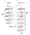
従来の一般的な樹脂めっき成膜方法は、図17に示すように、めっきする樹脂成形品に、その樹脂成形品の表面粗化するエッチング工程、エッチング中和工程、触媒付与工程、導電化工程(又は無電解めっき)等のダイレクトめっき前処理工程や化学めっき工程を施し、前処理した樹脂成形品に、光沢銅めっき、半光沢ニッケルめっき、光沢ニッケルめっき、MPニッケルめっき(マイクロポーラスニッケルめっき)の順で各めっき処理を施し、最後にクロムめっきを施して終了するめっき方法である。このように樹脂成形品は非導電性のため、電気めっきの前処理として樹脂に導電性を付与する導電化工程(ダイレクトめっき前処理又は無電解めっき)が必要である。
なお、従来の塗装用の樹脂成形品と、樹脂めっき用の樹脂成形品では、原料収縮率が異なるため塗装用の金型と樹脂めっき用の金型の2種類を準備する必要があった。
As shown in FIG. 17 , the conventional general resin plating film forming method includes an etching process for roughening the surface of the resin molded product, an etching neutralization process, a catalyst applying process, and a conductive process as shown in FIG. (Or electroless plating) or other direct plating pre-treatment process or chemical plating process, and pre-treated resin molded products are bright copper plating, semi-bright nickel plating, bright nickel plating, MP nickel plating (microporous nickel plating) In this order, each plating process is performed, and finally, chromium plating is performed, followed by finishing. Thus, since the resin molded product is non-conductive, a conductive step (direct plating pretreatment or electroless plating) for imparting conductivity to the resin is necessary as a pretreatment for electroplating.
It should be noted that a conventional resin molded product for coating and a resin molded product for resin plating have different raw material shrinkage rates, so two types of coating mold and resin plating mold have to be prepared.
一般的な湿式法による樹脂めっきをする樹脂成形品の導電化工程(又は無電解めっき)は、図18に示すように、高濃度のクロム酸(6価クロム)と硫酸の混酸を使用してエッチング処理し、水洗してからクロム酸中和し、水洗してからPd/Sn等の触媒付与し、水洗してから活性化して水洗した後に無電解めっきをする。 As shown in FIG. 18 , the conductive step (or electroless plating) of a resin molded product for resin plating by a general wet method uses a mixed acid of high concentration chromic acid (hexavalent chromium) and sulfuric acid. Etching treatment, washing with water, neutralizing with chromic acid, washing with water, applying a catalyst such as Pd / Sn, washing with water, activating and washing with water, followed by electroless plating.
樹脂成形品に無電解めっきを施す際のめっき前処理技術としては、例えば特許文献1の特開平5−132785号公報「無電解めっき前処理方法」のように、ガラス繊維を含有するポリイミド樹脂からなる絶縁物質の表面に無電解めっきを施すに際し前処理として行なわれる該絶縁物質のエッチング処理において、該絶縁物質の表面を無水クロム酸および硫酸を含有する溶液を用いてエッチング処理した後、ヒドラジンを含有する溶液でエッチング処理する二段エッチング処理を行なう無電解めっき前処理方法が提案されている。
この樹脂めっきの基本である樹脂の表面粗化する樹脂のエッチング工程は、現在でも高濃度のクロム酸(6価クロム)と硫酸の混酸が使用されている。このクロム酸を使ったエッチング工程はその廃液処理だけでなく、処理工程中の作業にも人体に悪影響を及ぼすおそれがあった。現在は、このクロム酸を使ったエッチング工程を樹脂めっき工程から廃止すべく様々な技術が提案されている。しかし、樹脂めっきの基本性能であるめっき密着性規格、例えば自動車部品規格の様な厳格な条件を充足する前処理が提案されていなかった。 The etching process of the resin that roughens the surface of the resin, which is the basis of this resin plating, still uses a mixed acid of high concentration chromic acid (hexavalent chromium) and sulfuric acid. This etching process using chromic acid has a risk of adversely affecting the human body not only in the waste liquid treatment but also in the work during the treatment process. At present, various techniques have been proposed to eliminate the etching process using chromic acid from the resin plating process. However, no pretreatment has been proposed that satisfies strict conditions such as plating adhesion standard, which is the basic performance of resin plating, for example, automotive parts standard.
例えば、PA樹脂(ポリアミド樹脂、6−ナイロン)の樹脂成形品は、塩酸系エッチング液を用いて樹脂の表面粗化をすることができる。POM樹脂(ポリアセタール)は、塩酸/硫酸混酸もしくはリン酸/硫酸混酸を用いてエッチングすることができる。LCP樹脂(液晶ポリマー)は、苛性カリエッチングを用いてエッチングすることができる。このように樹脂材料によっては、クロム酸系のエッチング液を使わないでエッチングすることが可能である。 For example, a resin molded product of PA resin (polyamide resin, 6-nylon) can be roughened using a hydrochloric acid-based etching solution. POM resin (polyacetal) can be etched using hydrochloric acid / sulfuric acid mixed acid or phosphoric acid / sulfuric acid mixed acid. The LCP resin (liquid crystal polymer) can be etched using caustic potash etching. Thus, depending on the resin material, it is possible to perform etching without using a chromic acid-based etchant.
PPE樹脂(ポリフェニルエーテル)のように比較的酸化に弱い樹脂の樹脂成形品については、過マンガン酸系のエッチング液を用いて表面粗化することが可能である。 For a resin molded product of a resin that is relatively vulnerable to oxidation, such as PPE resin (polyphenyl ether), the surface can be roughened using a permanganic acid-based etching solution.
ABS樹脂(アクリロニトリル/ブタジエン/スチレン樹脂)のような汎用樹脂の樹脂成形品は、マンガン酸系エッチング液を用いてエッチングすることができる。溶剤プリエッチング工程等を付加して過マンガン酸系エッチングのような弱いエッチング液でもエッチングすることができる。 A resin molded product of a general-purpose resin such as ABS resin (acrylonitrile / butadiene / styrene resin) can be etched using a manganic acid-based etchant. Etching can be performed with a weak etchant such as permanganic acid etching by adding a solvent pre-etching step or the like.
また、樹脂基材の導電化処理技術としては、例えば特許文献2の特開平6−212405号公報「ポリフェニレンサルファイド支持体上に銅をめっきする方法」のように、ポリフェニレンサルファイド支持体を、真空下にてRFアルゴンプラズマでエッチングする。真空を破ることなく、エッチングされた表面にチタンの層をスパッタリングし、そしてチタンによりスパッタリングされた表面に第1の銅層をスパッタリングし、スパッタリング手順の後、支持体に第2の銅層を所望の厚さに電気めっきする方法が提案されている。
この特許文献2のめっきする方法は、4.5〜5.5ポンド/インチの剥離強さが得られる。この方法は、EMIシールド用やプリント回路基板用の製品を造るのに有用であるとされている。
The plating method disclosed in
更に、樹脂成形品にスパッタリング処理する技術としては、例えば特許文献3の特表平9−511792号公報「負圧又は真空中において材料蒸気によって基板を被覆する装置」のように、材料蒸気源、及び陽極と陰極との間にプラズマを発生しかつ材料蒸気によって援助されるアーク放電内において材料蒸気をイオン化するために冷陽極と冷陰極とからなるイオン化装置が設けられており、その際、材料蒸気源とイオン化装置の陽極及び陰極とが、互いに電気的に切離されている、負圧又は真空中において材料蒸気によって基板を被覆する装置が提案されている。
従来のスパッタリング装置は、図19に示すように、真空チャンバー51内においてプラズマ放電により励起されたアルゴン等の衝突により金属ターゲット52より原子を飛び出させ、樹脂成形品(W)に成膜させる装置である。このスパッタリング処理により樹脂成形品Wに金属ターゲット52を成膜する。このスパッタリング装置では、平面的な形状の樹脂成形品W、又は凹凸のある形状であってものその片面のみを成膜処理する樹脂成形品Wでは、その樹脂成形品Wを装置内に固定するだけで十分であった。しかし、凹凸面を有する樹脂成形品Wにその表面に均一に成膜することができなかった。
As shown in FIG. 19 , the conventional sputtering apparatus is an apparatus that causes atoms to jump out of a
しかし、上述した湿式法のエッチング工程では、高濃度のクロム酸と硫酸との混酸のように様々な化学薬品を使用して導電化を行うため、樹脂成形品がこれらの薬品によって劣化することがあり、更に樹脂成形品の表面に薬品が残留するおそれがあった。その結果、樹脂めっきした製品の一部には樹脂成形品の表層薄膜が剥離し、その上のめっき膜と共に浮き上がり、めっき膜に亀裂が入ることがあった。この浮き上がっためっき膜は30〜50μm程度の金属膜で、その樹脂めっきした製品を使用したときにユーザーが指を切るなどの不具合が発生することがあった。 However, in the above-described wet etching process, various chemicals such as a mixed acid of chromic acid and sulfuric acid with a high concentration are used to conduct electrical conductivity, and the resin molded product may be deteriorated by these chemicals. In addition, there is a risk that chemicals may remain on the surface of the resin molded product. As a result, the surface layer thin film of the resin molded product peeled off on a part of the resin-plated product, and it floated together with the plating film thereon, and the plating film sometimes cracked. The floated plating film is a metal film of about 30 to 50 μm, and when the resin-plated product is used, a problem such as the user's finger being cut may occur.
また、樹脂成形品の樹脂素材によっては、上述したような湿式法による導電化処理できないか、あるいは困難な場合があった。例えば、自動車用ドアハンドルのめっきには、PC/ABS樹脂が主に用いられている。同じ製品の塗装用樹脂材料には、PC/PBTやPC/PETなどのPC/ポリエステル系の材料が使われており、用途別に材料が使い分けられている。これは、ドアハンドル用の樹脂材料としてはPC/ポリエステル系材料の方が適しているが、めっきが難しく、自動車仕様を満足できる樹脂めっきドアハンドルが作れないからである。 In addition, depending on the resin material of the resin molded product, there is a case where the conductive treatment by the wet method as described above cannot be performed or is difficult. For example, PC / ABS resin is mainly used for plating of automobile door handles. PC / polyester-based materials such as PC / PBT and PC / PET are used as the resin material for coating of the same product, and the materials are properly used according to applications. This is because although a PC / polyester material is more suitable as a resin material for the door handle, plating is difficult and a resin-plated door handle that satisfies the automotive specifications cannot be made.
エッチング工程で、高濃度のクロム酸と硫酸との混酸を使用するため作業環境が悪く、取り扱いも危険であった。無電解めっき工程で、発ガン性物質のホルマリンやアンモニアを使用するため作業環境が悪かった。また強い錯化剤を必要とするため、廃水処理が困難であった。各処理工程後に水洗工程を必要とするため、水の使用量が多いという問題を有していた。 Since the etching process uses a mixed acid of high concentration chromic acid and sulfuric acid, the working environment is poor and handling is also dangerous. The work environment was poor because formalin and ammonia, which are carcinogenic substances, were used in the electroless plating process. In addition, since a strong complexing agent is required, wastewater treatment has been difficult. Since a water washing step is required after each treatment step, there is a problem that the amount of water used is large.
一方、マグネトロン・スパッタリングなどの加速度を付けて樹脂に金属を叩き込む成膜方法も創案されているが、アルゴンで樹脂表面が叩かれて処理表面温度が高くなる可能性があり、ABS樹脂などのような低融点の材料は熱変形しやすいという問題を有していた。 On the other hand, a film deposition method in which a metal is struck into a resin with acceleration such as magnetron sputtering has been devised, but the surface of the resin may be struck by argon and the processing surface temperature may be increased, such as ABS resin. Such a low-melting-point material has a problem that it is easily deformed by heat.
グロー放電プラズマ法による成膜方法では、イオン化率が低く、十分な金属の加速ができないので樹脂めっき規格のピーリング密着強度は得られないという問題を有していた。 The film formation method by the glow discharge plasma method has a problem that the ionization rate is low and sufficient metal acceleration cannot be performed, so that the peeling adhesion strength of the resin plating standard cannot be obtained.
特許文献2、特許文献3に示すスパッタリング処理により樹脂成形品にターゲットの金属を成膜するスパッタリング装置では、基板のような平面的な形状の樹脂成形品、又は凹凸のある形状であってものその片面のみを成膜処理する技術であった。そこで、樹脂成形品では、その樹脂成形品を装置内に固定するだけで十分であった。しかし、凹凸面を有する樹脂成形品Wにその表面に均一に成膜することができないという問題を有していた。
In a sputtering apparatus for depositing a target metal film on a resin molded product by the sputtering process shown in
また、従来のスパッタリング装置では、吊り掛け治具に固定した樹脂成形品について、吊り掛け治具を回転するので、樹脂成形品の外周側は金属ターゲットに近づくことができる。一方、樹脂成形品の内周側は金属ターゲットに近づくことがない。そこで、樹脂成形品の外周側は常時金属が厚く成膜され、逆に樹脂成形品の内周側は金属が薄く成膜されやすく、スパッタリング金属の成膜厚が不均一になりやすいという問題を有していた。 Moreover, in the conventional sputtering apparatus, since the hanging jig is rotated with respect to the resin molded product fixed to the hanging jig, the outer peripheral side of the resin molded product can approach the metal target. On the other hand, the inner peripheral side of the resin molded product does not approach the metal target. Therefore, there is a problem that a metal film is always formed thick on the outer peripheral side of the resin molded product, and conversely, a thin metal film is easily formed on the inner peripheral side of the resin molded product, and the film thickness of the sputtering metal tends to be uneven. Had.
従来の樹脂成形品の装飾用途のクロムスパッタ法では、基材プラスチックの上にアンダーコートを施し、クロムスパッタを500〜1000Å程度ごく薄く成膜し、その上に保護コートであるトップコートを塗布する構造となっている。そのために皮膜の耐久力が乏しく、洗車ブラシなどによる磨耗や砂利によるチッピング・風雨や強い紫外線の影響にさらされる自動車用途には性能を満足せず使用が困難であった。 In the conventional chromium sputtering method for decorative use of resin molded products, an undercoat is applied on a base plastic, a chromium sputtering film is formed as thin as about 500 to 1000 mm, and a top coat as a protective coating is applied thereon. It has a structure. For this reason, the durability of the film is poor, and it has been difficult to use because it does not satisfy the performance in automobile applications exposed to the effects of abrasion with car wash brushes, chipping with gravel, wind and rain, and strong ultraviolet rays.
更に、樹脂成形品の上に性能向上のためハードコートなどの耐磨耗塗装をオーバーコートしたとしても、湿式電気めっき法による樹脂めっきの金属膜の耐久性・耐摩耗性には及ばないため、自動車部品のめっき用途には湿式の樹脂めっきが使われるのが通例であった。
従来の装飾用途のクロムスパッタ法では、アンダーコートやトップコート・ハードコート塗装に起因するゴミ・ブツなどの歩留り低下の不安が大きく、多額な投資で塗装用クリーンルームを設置する必要があった。
Furthermore, even if a hard coating or other wear-resistant coating is overcoated on the resin molded product to improve performance, it does not reach the durability and wear resistance of the metal film of resin plating by the wet electroplating method. In general, wet resin plating is used for plating automotive parts.
In the conventional chromium sputtering method for decorative use, there is a great deal of concern about the yield drop due to dust and solids due to undercoat, top coat, and hard coat painting, and it was necessary to install a clean room for painting with a large investment.
本発明は、かかる問題点を解決するために創案されたものである。すなわち、本発明の目的は、従来のエッチング工程と導電化工程におけるクロム酸と硫酸との混酸のような化学薬品を使用しない処理法、即ち乾式法により樹脂成形品に樹脂表面粗化をすると共に導電性を付与することで、このような化学薬品によって樹脂の表層が劣化することがなくなり、樹脂間剥離によるめっき浮き・割れが防止でき、樹脂めっき品の安全性は確保できる装飾めっき品の製造方法を提供することにもある。 The present invention has been developed to solve such problems. That is, the object of the present invention is to roughen the resin surface of a resin molded article by a treatment method that does not use chemicals such as a mixed acid of chromic acid and sulfuric acid in the conventional etching process and conductive process, that is, a dry process. Providing conductivity prevents the surface of the resin from being deteriorated by such chemicals, prevents plating floating and cracking due to peeling between resins, and manufactures decorative plated products that can ensure the safety of resin-plated products There is also to provide a method.
本発明の他の目的は、湿式電気めっき法による樹脂めっきの金属膜の耐久性・耐摩耗性を維持し、塗装用クリーンルームなどの多額な設備投資や、製品のゴミ・ブツなどの歩留り低下リスクが高い塗装工程を不要にすることにある。
本発明の成膜皮膜は真空チャンバー中でのスパッタされた金属と湿式電気めっきによる金属めっき膜であり、積層する膜はすべて金属となっており自動車用途に耐える耐磨耗性や耐久性などが付与可能である。また、塗装工程がないのでゴミ・ブツ不良を低減できる。従って、従来の一般的な湿式法による樹脂めっき法と装飾用クロムスパッタ法の欠点を同時に解消することができる装飾めっき品の製造方法を提供することにある。
Another object of the present invention is to maintain the durability and wear resistance of the resin-plated metal film by wet electroplating method, to make a large capital investment such as a clean room for painting, and to reduce the yield of products such as dust and scrap. This is to eliminate the need for a high painting process.
The film of the present invention is a sputtered metal in a vacuum chamber and a metal plating film by wet electroplating, and the films to be laminated are all metal and have wear resistance and durability that can withstand automotive applications. It can be granted. In addition, since there is no painting process, it is possible to reduce dust and defects. Accordingly, it is an object of the present invention to provide a method for producing a decorative plated product that can simultaneously eliminate the disadvantages of a conventional resin plating method by a wet method and a decorative chromium sputtering method.
また、本発明の目的は、樹脂成形品の変形抑制や低温でハイレートにスパッタリングができるように改良したスパッタリング装置を使用することで、乾式法で樹脂成形品に導電性を付与することにより、湿式法ではめっきが難しかった樹脂材料のめっきを可能にして、多種類の樹脂成形品の前処理工程を容易に実施することができる装飾めっき品の製造方法を提供することにもある。 In addition, the object of the present invention is to provide wetness by imparting conductivity to a resin molded product by a dry method by using a sputtering apparatus improved so that the deformation of the resin molded product can be suppressed and sputtering can be performed at a high rate at a low temperature. Another object of the present invention is to provide a method for producing a decorative plated product, which enables plating of a resin material, which is difficult to be plated by the method, and can easily perform a pretreatment process for various types of resin molded products.
本発明の製造方法によれば、スパッタリング装置内において、真空雰囲気状態で樹脂成形品(W)の表面をプラズマ処理で洗浄及び表面改質活性化する樹脂表面洗浄・活性化工程(S1)と、次に、同じくスパッタリング装置内において、前記樹脂成形品(W)の表面に、金属をスパッタリングにより樹脂との密着性を確保するために成膜する金属薄膜成膜工程(S2)と、続いて、前記金属薄膜成膜工程(S2)により樹脂成形品(W)に成膜した金属薄膜上に、スパッタリングにより導電化膜を成膜する導電化膜成膜工程(S4)と、前記導電化膜成膜工程(S4)が終了した樹脂成形品(W)を電気めっきする電気めっき工程と、から成り、樹脂成形品(W)の凹凸面に金属を均一に成膜する際に、前記スパッタリング装置内において樹脂成形品(W)を回転させながらその表面にスパッタリング処理する、ことを特徴とするスパッタリングによる樹脂導電化を利用した装飾めっき品の製造方法が提供される。 According to the manufacturing method of the present invention, in the sputtering apparatus, the resin surface cleaning / activation step (S1) for cleaning and surface modification activation of the surface of the resin molded article (W) by plasma treatment in a vacuum atmosphere state; Next, in the same sputtering apparatus, a metal thin film film forming step (S2) for forming a metal film on the surface of the resin molded product (W) to ensure adhesion with the resin by sputtering, A conductive film forming step (S4) for forming a conductive film by sputtering on the metal thin film formed on the resin molded product (W) by the metal thin film forming step (S2); and the conductive film forming step. An electroplating step of electroplating the resin molded product (W) after the film step (S4) is completed, and when the metal is uniformly formed on the uneven surface of the resin molded product (W), the inside of the sputtering apparatus In Sputtering process on the surface while rotating fat molded article (W), the manufacturing method of decorative plated products using resin conductive by sputtering, characterized in that there is provided.
例えば、スパッタリング装置内において、真空雰囲気状態で治具に取り付けた樹脂成形品(W)を自転するように回転させながらプラズマ処理で洗浄及び表面改質活性化する樹脂表面洗浄・活性化工程(S1)と、次に、同じくスパッタリング装置内において、治具に取り付けた樹脂成形品(W)を金属ターゲット(52)の前へ公転するように移動させ、そこで自転させながら、金属をスパッタリングにより樹脂との密着性を確保するために成膜する金属薄膜成膜工程(S2)と、続いて、前記金属薄膜成膜工程(S2)により金属薄膜を成膜した樹脂成形品(W)を別の金属ターゲット(52)の前に公転するように移動させ、そこで自転させながら、スパッタリングにより導電化膜を成膜する導電化膜成膜工程(S4)と、前記導電化膜成膜工程(S4)が終了した樹脂成形品(W)を電気めっきする電気めっき工程と、から成る装飾めっき品の製造方法である。
前記金属薄膜成膜工程(S2)の次に、樹脂成形品(W)に成膜した金属薄膜をプラズマ処理による表面改質処理で活性化する成膜表面活性化処理工程(S3)を更に備えることが好ましい。
For example, in a sputtering apparatus, a resin surface cleaning / activation step (S1) in which cleaning and surface modification activation are performed by plasma treatment while rotating a resin molded product (W) attached to a jig in a vacuum atmosphere so as to rotate. Next, in the same sputtering apparatus, the resin molded product (W) attached to the jig is moved so as to revolve in front of the metal target (52). A metal thin film forming step (S2) for forming a metal thin film in order to ensure the adhesion of the resin, and then, the resin molded product (W) formed with the metal thin film in the metal thin film forming step (S2) is replaced with another metal. Conductive film forming step (S4) of forming a conductive film by sputtering while revolving around the target (52) and rotating therewith, and the conductive And electroplating process for electroplating deposition step (S4) is finished resin molded article (W), a method for manufacturing a decorative plated products made of.
Subsequent to the metal thin film deposition step (S2), a film surface activation treatment step (S3) for activating the metal thin film deposited on the resin molded product (W) by surface modification treatment by plasma treatment is further provided. It is preferable.
前記スパッタリング装置の真空チャンバー内において、治具に樹脂成形品(W)を取り付け、その治具の回転軸線で回転させながらスパッタリング処理することが好ましい。
前記スパッタリング装置の真空チャンバー内において、複数の治具に樹脂成形品(W)を取り付け、各治具をその回転軸線で回転させながら、複数の治具をその回転軸が円形の軌跡上をなぞり、公転するように移動させてスパッタリング処理することが好ましい。
In the vacuum chamber of the sputtering apparatus, it is preferable to attach the resin molded product (W) to a jig and perform the sputtering treatment while rotating it around the rotation axis of the jig.
In the vacuum chamber of the sputtering apparatus, a resin molded product (W) is attached to a plurality of jigs, and the jigs are traced on a circular trajectory while the rotation axes of the jigs are rotated along their rotation axes. It is preferable to carry out sputtering treatment by moving it so as to revolve.
前記樹脂表面洗浄・活性化工程(S1)は、真空雰囲気内において、前記樹脂成形品(W)の表面に、空気を微量残留させた状態でプラズマ処理することが好ましい。
前記樹脂表面洗浄・活性化工程(S1)は、真空雰囲気内において、前記樹脂成形品(W)の表面に、アルゴンと微量酸素を注入してプラズマ処理による表面改質処理することが好ましい。
In the resin surface cleaning / activation step (S1), it is preferable to perform plasma treatment in a vacuum atmosphere in a state where a small amount of air remains on the surface of the resin molded product (W).
In the resin surface cleaning / activation step (S1), it is preferable to perform surface modification treatment by plasma treatment by injecting argon and a small amount of oxygen into the surface of the resin molded product (W) in a vacuum atmosphere.
例えば、前記金属薄膜成膜工程(S2)は、真空雰囲気内において、前記樹脂成形品(W)の表面に酸素との結合力が強い金属の単一又は酸素との結合力の強い金属を含む合金をスパッタリングにより成膜する。
例えば、前記金属薄膜成膜工程(S2)は、真空雰囲気内において、0.01〜50%にイオン化された金属を、前記樹脂成形品(W)の表面に成膜することができる。
前記金属薄膜成膜工程(S2)では、膜厚が0.01〜2.0μm程度になるように成膜する。
For example, the metal thin film forming step (S2) includes a single metal having a strong binding force with oxygen or a metal having a strong binding force with oxygen on the surface of the resin molded product (W) in a vacuum atmosphere. An alloy is deposited by sputtering.
For example, in the metal thin film forming step (S2), a metal ionized to 0.01 to 50% can be formed on the surface of the resin molded product (W) in a vacuum atmosphere.
In the metal thin film forming step (S2), the film is formed so that the film thickness is about 0.01 to 2.0 μm.
前記導電化膜成膜工程(S4)は、ニッケル又は銅を成膜することができる。
前記導電化膜成膜工程(S4)では、膜厚が0.1〜5.0μm程度になるように成膜することが好ましい。
In the conductive film formation step (S4), nickel or copper can be formed.
In the conductive film forming step (S4), it is preferable to form the film so that the film thickness is about 0.1 to 5.0 μm.
前記電気めっき工程は、光沢硫酸銅めっき(S6)、半光沢ニッケルめっき(S7)、光沢ニッケルめっき(S8)、MPニッケルめっき(マイクロポーラスニッケルめっき)(S9)の順で各めっき処理を施し、最後に装飾仕上げめっき(S10)を施してめっき処理を終了することができる。
例えば、前記装飾仕上げめっき(S10)では、3価クロムめっき、クロムめっき、錫/ニッケル合金めっき、ルテニウム又は金めっきなどのめっき処理を施す。
In the electroplating step, each copper plating treatment is performed in the order of bright copper sulfate plating (S6), semi-bright nickel plating (S7), bright nickel plating (S8), MP nickel plating (microporous nickel plating) (S9), Finally, the decorative finish plating (S10) can be performed to finish the plating process.
For example, in the decorative finish plating (S10), a plating treatment such as trivalent chromium plating, chromium plating, tin / nickel alloy plating, ruthenium or gold plating is performed.
上述したように、本発明の製造方法では、樹脂表面洗浄・活性化工程(S1)においてスパッタリング装置内で、樹脂成形品(W)の表面を、プラズマ処理で洗浄及び表面改質活性化し、次に、金属薄膜成膜工程(S2)で同じくスパッタリング装置内で、酸素との結合力の強い金属の単一、又は酸素との結合力の強い金属を含む合金を、成膜し、続いて、導電化膜成膜工程(S4)でこの樹脂成形品(W)に成膜した金属薄膜上に、所定の金属をスパッタリングにより導電化膜を成膜することで、乾式法により樹脂成形品(W)に成膜を行い導電性を付与することができる。そこで、従来の湿式法では不可能であった新素材特殊材料に低温で成膜できるので、従来のように加熱により樹脂成形品(W)が軟化し、更に変形するといった不具合を防止することができる
スパッタリング装置内において、凹凸面を有する樹脂成形品(W)を回転させながらその表面にスパッタリング処理することにより、その表面に金属を均一に成膜することができる。
As described above, in the production method of the present invention, the surface of the resin molded product (W) is cleaned and activated by the plasma treatment in the sputtering apparatus in the resin surface cleaning / activation step (S1). In addition, in the metal thin film forming step (S2), in the same sputtering apparatus, a single metal having a strong binding force with oxygen or an alloy containing a metal having a strong binding force with oxygen is formed, A conductive film is formed by sputtering a predetermined metal on the metal thin film formed on the resin molded product (W) in the conductive film forming step (S4), thereby forming a resin molded product (W ) To provide conductivity. Therefore, since it is possible to form a film on a new special material, which was impossible with the conventional wet method, at a low temperature, it is possible to prevent the problem that the resin molded product (W) is softened and further deformed by heating as in the past. In the sputtering apparatus, a metal film can be uniformly formed on the surface of the resin molded product (W) having an uneven surface by rotating the surface while rotating the surface.
更に、電気めっき後あるいは乾式法めっき後の最外層に高付加・高機能膜(透明性保護膜、高硬度膜など)を付与することができるため、乾式法を利用しためっき前処理技術以外の表面処理技術としての応用が可能である。
樹脂との密着性を得る目的で処理する金属薄膜成膜工程(S2)の次に成膜表面活性化処理工程(S3)を付け加えることで、導電化膜成膜工程(S4)の際に処理する導電化膜の密着力が強固になる。
導電化膜成膜工程(S4)の次に通常の樹脂めっきと同様な電気めっきを施すだけで、最終の樹脂めっき製品を生産することができる。
Furthermore, since it is possible to provide high-addition and high-functional films (transparency protective film, high hardness film, etc.) on the outermost layer after electroplating or after dry process plating, other than plating pretreatment technology using dry process Application as surface treatment technology is possible.
Process is performed during the conductive film deposition step (S4) by adding a film surface activation treatment step (S3) after the metal thin film deposition step (S2) for the purpose of obtaining adhesion with the resin. The adhesion strength of the conductive film is strengthened.
The final resin-plated product can be produced simply by performing electroplating similar to normal resin plating after the conductive film forming step (S4).
また、樹脂めっきの前処理、即ち樹脂成形品(W)の導電化処理について、従来のような6価クロムを用いる湿式法から乾式法に変更することにより、樹脂めっき製造における環境負荷が大きい化学薬品を使用する湿式導電化処理ではないため、環境負荷物質を激減することができる。従来のように、6価クロム等の廃液処理が不必要又は激減することができる。 In addition, the pretreatment of the resin plating, that is, the conductive treatment of the resin molded product (W), is changed from a conventional wet method using hexavalent chromium to a dry method, thereby increasing the environmental impact in resin plating production. Since it is not a wet conductive process using chemicals, environmentally hazardous substances can be drastically reduced. As in the past, waste liquid treatment such as hexavalent chromium can be unnecessary or drastically reduced.
本発明のスパッタリングによる樹脂導電化を利用した装飾めっき品の製造方法は、樹脂めっきの湿式導電化法を乾式導電化法へ変更した前処理方法である。その導電化後は通常通り湿式電気めっきする。 The method for producing a decorative plating product using resin conductivity by sputtering according to the present invention is a pretreatment method in which the wet electroconducting method of resin plating is changed to the dry electroconducting method. After the conductivity, wet electroplating is performed as usual.
以下、本発明の好ましい実施の形態を図面を参照して説明する。
図1は実施例1のスパッタリングによる樹脂導電化を利用した装飾めっき品の製造方法を示す工程図である。図2は光沢ニッケルめっき方法の一例を示すものであり、(a)は樹脂導電化処理の工程図、(b)は湿式電気めっき工程図である。
本発明の実施例1のスパッタリングによる樹脂導電化を利用した装飾めっき品の製造方法は、樹脂成形品Wを治具にセットし、樹脂表面洗浄・活性化工程S1で、スパッタリング装置内において、真空雰囲気状態で樹脂成形品Wの表面をプラズマ処理で洗浄及び表面改質活性化し、次に、金属薄膜成膜工程S2で、同じくスパッタリング装置内において、樹脂成形品Wの表面に、酸素との結合力の強い金属の単一、又は酸素との結合力の強い金属を含む合金を、をスパッタリングにより成膜し、続いて金属薄膜成膜工程S2の次の成膜表面活性化処理工程S3で、樹脂成形品Wに成膜した金属薄膜をプラズマ処理による表面改質処理で活性化し、最後に導電化膜成膜工程S4で、樹脂成形品Wに成膜した金属薄膜上に、所定の金属をスパッタリングにより導電化膜を成膜する方法である。
このように、乾式法のマグネトロン・スパッタ法等により、樹脂成形品Wの表面改質と金属成膜を行い、導電性を付与する。この樹脂導電化処理を施した樹脂成形品Wは治具から取り外し、後述するように電気めっき工程S5〜S10で電気めっき処理を施す。
Hereinafter, preferred embodiments of the present invention will be described with reference to the drawings.
FIG. 1 is a process diagram showing a method of manufacturing a decorative plated product using resin conduction by sputtering in Example 1. 2A and 2B show an example of the bright nickel plating method. FIG. 2A is a process diagram of resin conductive treatment, and FIG. 2B is a wet electroplating process diagram.
In the method for producing a decorative plated product using resin conduction by sputtering according to the first embodiment of the present invention, the resin molded product W is set on a jig, and the resin surface cleaning / activation step S1 is performed in a vacuum in the sputtering apparatus. In the atmosphere state, the surface of the resin molded product W is cleaned by plasma treatment and activated for surface modification. Next, in the metal thin film deposition step S2, oxygen is bonded to the surface of the resin molded product W in the same sputtering apparatus. A single strong metal or an alloy containing a metal having a strong binding force with oxygen is formed by sputtering, and subsequently in a film formation surface activation treatment step S3 subsequent to the metal thin film formation step S2, The metal thin film formed on the resin molded product W is activated by surface modification treatment by plasma treatment, and finally a predetermined metal is applied on the metal thin film formed on the resin molded product W in the conductive film forming step S4. Spatter A method of forming a conductive film by packaging.
In this manner, the surface of the resin molded product W is reformed and the metal film is formed by a dry-type magnetron sputtering method or the like to impart conductivity. The resin molded product W subjected to the resin conductive treatment is removed from the jig and subjected to electroplating in electroplating steps S5 to S10 as described later.
マグネトロン・スパッタリングで用いるスパッタリング装置は、真空雰囲気内においてプラズマ放電により励起されたアルゴン等の衝突によりタ金属ターゲットから原子を飛び出させ、樹脂成形品Wに成膜させる装置である。このスパッタリング処理により樹脂成形品Wにターゲットの金属を成膜し、または樹脂成形品Wにプラズマを照射する。 A sputtering apparatus used in magnetron sputtering is an apparatus that deposits atoms on a metal target W by depositing atoms from a metal target by collision of argon or the like excited by plasma discharge in a vacuum atmosphere. A film of a target metal is formed on the resin molded product W by this sputtering treatment, or the resin molded product W is irradiated with plasma.
本発明の装飾めっき品となる樹脂成形品Wは、自動車用樹脂めっき部品、シャワーや蛇口部品等の住宅関連樹脂めっき部品等のいわゆる「外観製品」である。従来の装飾めっき品の製造方法では樹脂成形品Wの樹脂間剥離でめっき膜が浮き上がり、手を切るなどの人身致傷の原因なることがあったので、「外観製品」の外観の仕上がりは重要である。因みに、プリント基板のような「機能製品」であれば、このような装飾めっきを施す必要はない。 The resin molded product W, which is a decorative plated product of the present invention, is a so-called “appearance product” such as a resin-plated component for automobiles and a housing-related resin-plated component such as a shower or faucet component. In the conventional method for producing decorative plated products, the plating film floats up due to the separation of the resin molded product W between the resins, which may cause personal injury such as cutting hands. Therefore, the appearance of the “appearance product” is important. is there. Incidentally, if it is a “functional product” such as a printed circuit board, it is not necessary to apply such decorative plating.
樹脂表面洗浄・活性化工程S1では、真空度を例えば10−1(=10の−1乗)Pa程度の真空チャンバーのような真空雰囲気内で樹脂表面をプラズマ処理により洗浄及び表面改質活性化する。例えば、空気を微量残留させた状態でアルゴンプラズマ処理する。又はアルゴンと微量酸素を注入してのプラズマ処理をする。
この樹脂表面洗浄・活性化工程S1は、マグネトロン・スパッタ法の他に、アークプラズマ蒸着法でのプラズマ処理法を使用することができる。
In the resin surface cleaning / activation step S1, the resin surface is cleaned and activated by plasma treatment in a vacuum atmosphere such as a vacuum chamber with a degree of vacuum of about 10 −1 (= 10 −1) Pa, for example. To do. For example, argon plasma treatment is performed with a minute amount of air remaining. Alternatively, plasma treatment is performed by injecting argon and trace oxygen.
In this resin surface cleaning / activation step S1, a plasma processing method using an arc plasma deposition method can be used in addition to the magnetron sputtering method.
金属薄膜成膜工程S2は、真空チャンバーのような真空雰囲気内でマグネトロン・スパッタ法により、樹脂とめっき膜との密着性を確保するための工程である。真空度を例えば10−2〜3(10の−2〜3乗)Pa程度に引き上げ、プラズマによって0.01〜50%にイオン化されたクロム、モリブデン、タングステン、チタン、ジルコニウム、アルミニウム、インジウム、ニッケル、パラジウムなどの酸素との結合力の強い金属(親酸素金属)の単一もしくは、それらの金属を含む合金を樹脂成形品Wに成膜する。 The metal thin film forming step S2 is a step for securing the adhesion between the resin and the plating film by magnetron sputtering in a vacuum atmosphere such as a vacuum chamber. Chromium, molybdenum, tungsten, titanium, zirconium, aluminum, indium, nickel ionized to 0.01 to 50% by plasma after raising the degree of vacuum to, for example, about 10 −2 to 3 (10 −2 to the third power) Pa. On the resin molded product W, a single metal (oxygen metal) having a strong binding force with oxygen such as palladium or an alloy containing these metals is formed.
また、金属薄膜成膜工程S2では、ニッケルクロム合金(合金比=50:50)や金属クロムを用いることが好ましい。樹脂とめっき膜との密着性を確保するための金属薄膜は、樹脂との密着性が良好なだけではなく、次工程の電気めっきを円滑に処理するための導電化膜との密着性が良好な金属を使用する必要がある。金属薄膜成膜工程S2では、クロム単体、クロム・ニッケル合金、アルミニウム、銅合金などを使用することが好ましい。合金比率は特に規定しない。樹脂の種類や成形条件等によって密着の良い成膜金属材料を選択する。例えば金属銅を使用することができる。めっき密着力を確保するための膜厚に制限はないが、めっき応力等を考えると0.05μm〜0.5μmが適当であった。 Further, in the metal thin film forming step S2, it is preferable to use a nickel chromium alloy (alloy ratio = 50: 50) or metal chromium. The metal thin film for ensuring the adhesion between the resin and the plating film not only has good adhesion with the resin, but also has good adhesion with the conductive film for smooth electroplating in the next process. It is necessary to use a new metal. In the metal thin film forming step S2, it is preferable to use chromium alone, chromium / nickel alloy, aluminum, copper alloy or the like. The alloy ratio is not specified. A film-forming metal material with good adhesion is selected depending on the type of resin, molding conditions, and the like. For example, metallic copper can be used. Although there is no restriction | limiting in the film thickness for ensuring plating adhesive force, 0.05 micrometer-0.5 micrometer were suitable when plating stress etc. were considered.
金属薄膜成膜工程S2が終了した樹脂成形品Wに、更に成膜表面活性化処理工程S3で活性化処理を施すことが好ましい。例えば、樹脂成形品Wに0.01μm〜2.0μmで成膜した金属薄膜をアルゴンプラズマ処理による表面改質処理で活性化する。これにより樹脂成形品Wと金属薄膜との密着力が高くなる。 It is preferable that the resin molded product W that has undergone the metal thin film formation step S2 is further subjected to an activation process in the film formation surface activation process step S3. For example, a metal thin film formed on the resin molded product W at a thickness of 0.01 μm to 2.0 μm is activated by a surface modification process using an argon plasma process. Thereby, the adhesive force of the resin molded product W and a metal thin film becomes high.
導電化膜成膜工程S4は、樹脂成形品Wに電気めっき処理するための導電化膜を成膜する工程である。電気めっき用の導電化膜は、電気めっき処理するための導電化膜であるが、乾式めっき法で形成しためっき膜と電気めっき法で成膜する膜とのめっき密着性を確保するための酸処理や希薄な酸化剤によるソフトエッチングもしくは、電解活性化処理に耐えうる金属膜である必要がある。そこで、この導電化膜成膜工程S4による膜厚は、例えば金属銅の場合は0.5μmから2.0μmが適当であった。この導電化膜成膜工程S4による成膜は、下層金属との密着力が良く、更に後工程である湿式電気めっき(電気銅めっきや電気ニッケルめっき)の前処理(活性化工程)S5が簡単で密着性も高い金属であれば金属銅以外の金属を成膜することができる。 The conductive film forming step S4 is a step of forming a conductive film for electroplating the resin molded product W. The electroconductive film for electroplating is a electroconductive film for electroplating, but it is an acid for ensuring plating adhesion between a plating film formed by a dry plating method and a film formed by an electroplating method. The metal film must be able to withstand the treatment, soft etching with a dilute oxidizing agent, or electrolytic activation treatment. Therefore, the thickness of the conductive film forming step S4 is suitably 0.5 μm to 2.0 μm in the case of metallic copper, for example. Film formation by this conductive film forming step S4 has good adhesion to the lower layer metal, and simple pretreatment (activation step) S5 of wet electroplating (electrocopper plating or electronickel plating) as a subsequent step. If the metal has high adhesion, a metal other than metallic copper can be formed.
このように樹脂表面洗浄・活性化工程S1、金属薄膜成膜工程S2及び導電化膜成膜工程S4が終了した乾式めっきで導電化処理まで終わった樹脂成形品は、真空チャンバーから取り出し、電気めっき用の治具に掛け替えて通常の電気めっき工程で仕上げる。 Thus, after the resin surface cleaning / activation step S1, the metal thin film formation step S2, and the conductive film formation step S4 are finished, the resin molded product that has been subjected to the conductive treatment is removed from the vacuum chamber and electroplated. Finish with a normal electroplating process.
湿式電気めっきでは、図2(b)に示すように、マグネトロン・スパッタリングにより樹脂導電化処理を施した樹脂成形品Wを活性化工程S5で乾式めっき膜を活性化する。この活性化工程S5は、電気めっきとの密着を確保するための工程である。例えば、乾式めっきの最終導電化金属として銅を用いたときは、20g/Lの過硫酸Na溶液に30秒間浸漬するソフトエッチング工程でおこなった。なお、この活性化工程S5は、乾式めっきで使う導電化金属の種類によって様々な方法がある。乾式めっき膜と電気めっき膜との密着性が確保できる方法であれば、その方法は限定しない。 In the wet electroplating, as shown in FIG. 2B, the dry-plated film is activated in the activation step S5 of the resin molded product W that has been subjected to the resin conductive treatment by magnetron sputtering. This activation step S5 is a step for ensuring close contact with electroplating. For example, when copper was used as the final conductive metal in the dry plating, it was performed in a soft etching step that was immersed in a 20 g / L Na persulfate solution for 30 seconds. Note that there are various methods for the activation step S5 depending on the type of conductive metal used in the dry plating. The method is not limited as long as the adhesion between the dry plating film and the electroplating film can be ensured.
電気めっき工程S6〜S10は光沢硫酸銅めっき等通常の樹脂めっきや金属めっきに用いられる電気めっきが適応できる。例えば図示するように光沢硫酸銅めっきS6、半光沢ニッケルめっきS7、光沢ニッケルめっきS8、MPニッケルめっき(マイクロポーラスニッケルめっき)S9の順で各めっき処理を施す。
最後に3価クロムめっき、錫/ニッケル合金めっき、ルテニウム又は金めっきなどの装飾仕上げめっきS10を施してめっき処理を終了する。勿論、従来から利用されている6価クロムからのクロムめっきも使用可能である。
この電気めっき工程S6〜S10は一例であって、これ以外の金属をめっき処理できることは勿論である。
The electroplating steps S6 to S10 can be applied to normal resin plating such as bright copper sulfate plating or electroplating used for metal plating. For example, as shown in the drawing, each of the plating processes is performed in the order of bright copper sulfate plating S6, semi-bright nickel plating S7, bright nickel plating S8, and MP nickel plating (microporous nickel plating) S9.
Finally, a decorative finish plating S10 such as trivalent chromium plating, tin / nickel alloy plating, ruthenium or gold plating is applied to finish the plating process. Of course, chromium plating from hexavalent chromium which has been conventionally used can also be used.
These electroplating steps S6 to S10 are merely examples, and it is a matter of course that other metals can be plated.
図3は実施例1のスパッタリングによる樹脂導電化処理した樹脂成形品の断面図である。図4は実施例1のスパッタリングによる樹脂導電化を利用した装飾めっき品の製造方法によりめっきしためっき被膜の断面図である。
光沢硫酸銅めっき30μm、半光沢ニッケルめっき10μm、光沢ニッケルめっき10μm、マイクロポーラスニッケルめっき1.3μm、クロムめっき0.35μm程度の電気めっきを行い、後述するピーリング密着試験や、サーマルサイクル試験等の樹脂めっき機能試験を実施し、めっき製品の評価を行った。
FIG. 3 is a cross-sectional view of a resin molded product subjected to resin conductivity treatment by sputtering in Example 1. FIG. 4 is a cross-sectional view of a plating film plated by the method of manufacturing a decorative plating product using resin conduction by sputtering in Example 1.
Electroplating of bright copper sulfate plating 30μm, semi-bright nickel plating 10μm, bright nickel plating 10μm, microporous nickel plating 1.3μm, chromium plating 0.35μm, and resin for peeling adhesion test and thermal cycle test described later A plating function test was conducted to evaluate the plated product.
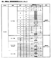
本発明の実施例1のスパッタリングによる樹脂導電化を利用した装飾めっき品の製造方法によりめっきした製品のめっきの密着力に関する実験について説明する。図5は「表1 プレート密着測定結果」を示す表である。図6は「表2 スパッタリング実験条件」を示す表である。図7は「表3 実製品密着測定結果(Ni−Cr)No1」を示す表である。図8は「表4 実製品密着測定結果(Ni−Cr)No2」を示す表である。図9は「表5 実製品密着測定結果(Cr)」を示す表である。
(1)予備試験(樹脂プレート)
樹脂プレートを使って材料別の密着強度、成膜前の樹脂の表面洗浄・活性化に酸素注入の効果があるか、樹脂材料による差、無機フィラーの影響等を概略的に調べた結果を図5の「表1 プレート密着測定結果」に示した。この表1の結果のように樹脂表面洗浄処理時の酸素ガス注入によって密着性が向上することがわかった。但し、ABS樹脂プレートに関しては酸素ガス注入の効果は高くなかった。ABS樹脂プレート試験には樹脂厚みを変えた3段プレート(ゲート=3mm/2mm/1mm=下段)を使って試験をおこなった。膜厚が厚いところの方が密着力が高く、形状や成形条件でも密着が変化することを予測させる結果となった。材料的には、ナイロン系、ABS系の樹脂の密着強度が高いことがわかった。
An experiment relating to the adhesive strength of plating of a product plated by a method for producing a decorative plated product using resin conduction by sputtering in Example 1 of the present invention will be described. FIG. 5 is a table showing “Table 1 Plate Adhesion Measurement Results”. FIG. 6 is a table showing “Table 2 Sputtering Experiment Conditions”. FIG. 7 is a table showing “Table 3 Actual Product Adhesion Measurement Results (Ni—Cr) No1”. FIG. 8 is a table showing “Table 4 Actual Product Adhesion Measurement Results (Ni—Cr) No. 2”. FIG. 9 is a table showing “Table 5 Actual Product Contact Measurement Results (Cr)”.
(1) Preliminary test (resin plate)
Fig. 3 shows the results of a rough investigation of the adhesion strength by material using a resin plate, whether there is an oxygen injection effect on the surface cleaning and activation of the resin before film formation, the difference depending on the resin material, the influence of inorganic fillers, etc. The results are shown in “Table 1 Plate Adhesion Measurement Results”. As shown in Table 1, it was found that the adhesion was improved by oxygen gas injection during the resin surface cleaning treatment. However, the effect of oxygen gas injection was not high for the ABS resin plate. The ABS resin plate test was performed using a three-stage plate (gate = 3 mm / 2 mm / 1 mm = lower stage) with different resin thicknesses. The thicker the film, the higher the adhesion force, and the result of predicting that the adhesion changes even with the shape and molding conditions. In terms of materials, it was found that the adhesion strength of nylon and ABS resins was high.
(2)実成形品での試験結果
試験条件を図6の「表2 スパッタリング実験条件」に示した。めっき密着性用成膜金属はニッケル・クロム合金(合金比=50:50)とクロム(99.9%)品の2種類の試験をおこなった。導電化膜は金属銅(99.9%)をターゲットとして使用した。
(2) Test results on actual molded products The test conditions are shown in "Table 2 Sputtering experiment conditions" in FIG. The metal film for plating adhesion was subjected to two types of tests: nickel / chromium alloy (alloy ratio = 50: 50) and chromium (99.9%). The conductive film used metal copper (99.9%) as a target.
(3)実製品密着測定結果
図7〜図9の「表3 実製品密着測定結果(Ni−Cr)No1」、「表4 実製品密着測定結果(Ni−Cr)No2」にニッケル・クロム合金での結果を、「表5 実製品密着測定結果(Cr)」にクロムでの結果を示した。
「表2 スパッタリング実験条件」に示した実験条件4、実験条件8、実験条件10の条件で密着力の高い樹脂めっきが作れることがわかった。特に、PA/ABS樹脂は密着力がmax4.75Kgf/cm=約47N/cmの高い数値を示した。その他の材料でも適正な条件を選択すれば量産化が可能である。
(3) Actual product adhesion measurement results
The results of nickel-chromium alloy are shown in "Table 3 Actual product adhesion measurement result (Ni-Cr) No1" and "Table 4 Actual product adhesion measurement result (Ni-Cr) No2" in Figs. Actual product adhesion measurement results (Cr) "show the results for chromium.
It was found that resin plating with high adhesion can be made under the conditions of
(4)サーマルショック試験結果
PC/ABS樹脂めっき試作品(Ni/Cr実験条件10の製品)及びPA/ABS樹脂めっき試作品(同じ条件)を−30℃/0.5Hr⇒80℃/0.5Hrを1サイクルとして、120サイクルのサーマルショック試験をおこなったが、パート部分の樹脂層薄膜剥離によるめっき浮き現象は確認されなかった。従って、本発明の方法を使えば安全な樹脂めっき部品を量産化できることがわかった。
(4) Thermal Shock Test Results PC / ABS resin plating prototype (product under Ni / Cr experimental condition 10) and PA / ABS resin plating prototype (same conditions) were −30 ° C./0.5 Hr → 80 ° C./0.00. A thermal shock test of 120 cycles was performed with 5Hr as one cycle, but no plating floating phenomenon due to the resin layer thin film peeling of the part portion was confirmed. Therefore, it was found that safe resin-plated parts can be mass-produced by using the method of the present invention.
本発明のスパッタリングによる樹脂導電化を利用した装飾めっき品の製造方法は、樹脂めっきの前処理にスパッタリングの乾式めっき法を利用していので、従来のクロム酸による導電化処理法と異なり種々の樹脂を対象とすることができる。例えば、ABS樹脂(アクリロニトリル/ブタジエン/スチレン)、PC/ABS樹脂(ポリカーボネイト/アクリロニトリル/ブタジエン/スチレン)、PC/PET樹脂(ポリカーボネイト/ポリエチレンテレフタレート)、PC/PBT樹脂(ポリカーボネイト/ポリブチレンテレフタレート)、LCP樹脂(液晶ポリマー)、PA樹脂(ポリアミド)、PA/ABS(ポリアミド/アクリロニトリル/ブタジエン/スチレン)、PPE樹脂(ポリフェニレンエーテル)、PP樹脂(ポリプロピレン)、PPS樹脂(ポリフェニレンサルファイド)、SPS樹脂(結晶性ポリスチレン)、PS樹脂(ポリスチレン)、MMA樹脂(メタクリル酸メチル)、エポキシ樹脂、ウレタン樹脂、PET樹脂(ポリエチレンテレフタレート)、PBT樹脂(ポリブチレンテレフタレート)、PC樹脂(ポリカーボネイト)等がある。更にこれらの樹脂のポリマーアロイも対象とすることができる。 The method for producing a decorative plating product using resin conduction by sputtering according to the present invention uses a dry plating method of sputtering for pre-treatment of resin plating, and therefore various resins are different from the conventional conductive treatment method by chromic acid. Can be targeted. For example, ABS resin (acrylonitrile / butadiene / styrene), PC / ABS resin (polycarbonate / acrylonitrile / butadiene / styrene), PC / PET resin (polycarbonate / polyethylene terephthalate), PC / PBT resin (polycarbonate / polybutylene terephthalate), LCP Resin (liquid crystal polymer), PA resin (polyamide), PA / ABS (polyamide / acrylonitrile / butadiene / styrene), PPE resin (polyphenylene ether), PP resin (polypropylene), PPS resin (polyphenylene sulfide), SPS resin (crystalline) Polystyrene), PS resin (polystyrene), MMA resin (methyl methacrylate), epoxy resin, urethane resin, PET resin (polyethylene terephthalate), PBT resin Polybutylene terephthalate), a PC resin (polycarbonate) or the like. Furthermore, polymer alloys of these resins can also be targeted.
特にナイロン系樹脂と乾式めっき膜との密着性が良い。ナイロン系樹脂は、湿式めっきでは塩酸等のエッチング処理により製品表面が荒れてしまい綺麗なめっき外観が得ることが難しい材料であるが、乾式法では製品外観が悪くなることはなくABS樹脂めっき品のような綺麗な外観を得ることができた。 In particular, the adhesion between the nylon resin and the dry plating film is good. Nylon-based resin is a material that is difficult to obtain a beautiful plating appearance by wet plating, and the product surface is roughened by etching treatment with hydrochloric acid or the like. It was possible to obtain such a beautiful appearance.
一般的に樹脂めっきに使用されるABS樹脂においても1Kgf/cm(9.8N/cm)以上のめっき密着力が得られた。本発明の乾式めっきを利用した樹脂めっき前処理工程(樹脂の導電化工程)では、めっき密着強度をピーリング強度で0.5Kgf/cm(4.9N/cm)を合格目標値として試験をおこなった。なお、自動車規格では1.0Kgf/cm(9.8N/cm)を努力目標値として設定されているが、実使用上0.5Kgf/cm(4.9N/cm)で使用可能である。 Even in an ABS resin generally used for resin plating, a plating adhesion of 1 kgf / cm (9.8 N / cm) or more was obtained. In the resin plating pretreatment process (resin electroconducting process) using dry plating according to the present invention, the plating adhesion strength was tested with a peeling strength of 0.5 kgf / cm (4.9 N / cm) as an acceptable target value. . In the automobile standard, 1.0 kgf / cm (9.8 N / cm) is set as an effort target value, but it can be used at 0.5 kgf / cm (4.9 N / cm) in actual use.
乾式めっき前に樹脂のクリーニングと共に、酸素プラズマ(空気によるプラズマ処理を含む)処理をすることにより、密着性が向上することができる。但し、その条件は樹脂や成形条件によって変更する必要がある。 Adhesion can be improved by performing oxygen plasma (including plasma treatment with air) treatment together with resin cleaning before dry plating. However, the conditions need to be changed depending on the resin and molding conditions.
樹脂めっきの前処理(樹脂の導電化処理)を従来の6価クロムを用いる湿式法から乾式法に変更することで樹脂めっき製造における環境負荷は激減すると考える。 It is thought that the environmental burden in resin plating production will be drastically reduced by changing the pretreatment of resin plating (resin conductive treatment) from the conventional wet method using hexavalent chromium to the dry method.
[樹脂表面洗浄・活性化工程後の表面観察]
樹脂表面洗浄・活性化工程S1を実施した後の表面観察を走査型電子顕微鏡SEM(Scanning Electron Microscope)およびAFM(Atomic Force Microscope;原子間力顕微鏡)を用いて行った。
SEM観察結果を図10に、AFM観察結果を図11に示す。
SEM観察ではプラズマ未処理と処理表面との差が不明瞭であったが、AFM観察ではプラズマ処理を行うことで、樹脂表面に凹凸が出来ることが確認することができた。
従来の樹脂めっきでは、このSEM像程度の凹凸ではめっきのアンカー効果が得られないため、自動車部品規格を満足するめっき密着力は得られるものではないが、本方法では現状程度の表面凹凸で自動車部品規格を満足する密着力が得られている。
[Surface observation after resin surface cleaning / activation process]
Surface observation after the resin surface cleaning / activation step S1 was performed was performed using a scanning electron microscope SEM (Scanning Electron Microscope) and an AFM (Atomic Force Microscope).
The SEM observation result is shown in FIG. 10 , and the AFM observation result is shown in FIG .
In SEM observation, the difference between the untreated plasma and the treated surface was unclear, but in AFM observation, it was confirmed that unevenness was formed on the resin surface by performing the plasma treatment.
With conventional resin plating, the plating anchor effect cannot be obtained with the unevenness of about this SEM image, so plating adhesion that satisfies the automotive parts standard cannot be obtained. Adhesive strength that satisfies parts standards is obtained.
プラズマ処理品と未処理品の表面について、ぬれ張力試験混合液(関東化学(株)製)を用いてぬれ張力試験を実施したところ、いずれの樹脂(PA,PA/ABS,PC/ABS,ABS,PP,PC/PET)においてもぬれ性が向上した。このことから、プラズマ処理により樹脂表面に親水性官能基が生成しているものと思われる。
この官能基が金属薄膜成膜工程S2のスパッタリング金属が化学結合することで樹脂との密着力が発生する。
When wetting tension test was performed on the surface of the plasma treated product and the untreated product using a wet tension test mixed solution (manufactured by Kanto Chemical Co., Ltd.), any resin (PA, PA / ABS, PC / ABS, ABS) , PP, PC / PET) also improved wettability. From this, it is considered that a hydrophilic functional group is generated on the resin surface by the plasma treatment.
This functional group chemically bonds with the sputtered metal in the metal thin film forming step S2, thereby generating an adhesive force with the resin.
図12の「表21 イオン照射処理の実験結果」にPA/ABS(PA比率50%,70%,フィラー入り)とPC/ABS,PC/PETの自動車内装ドアハンドル製品について種々のプラズマ処理(樹脂表面洗浄・活性化工程S1)条件の実験を行った結果を示す。
その結果、原料によって密着の良い条件と悪い条件があり、原料によってプラズマ処理条件を選択する必要があることが分かった。また、ドアハンドルのRH(右側)とLH(左側)でも、密着力が大きく異なる場合もあることから、成形の条件によっても密着力が異なることが分かった。
Various plasma treatments (resins) for automotive interior door handle products of PA / ABS (PA ratio 50%, 70%, with filler) and PC / ABS, PC / PET are listed in "Table 21 Experimental results of ion irradiation treatment" in FIG. Surface cleaning / activation step S1) The results of experiments on conditions are shown.
As a result, it was found that there are good and bad adhesion conditions depending on the raw material, and it is necessary to select plasma treatment conditions depending on the raw material. In addition, the adhesion force may differ greatly between the RH (right side) and LH (left side) of the door handle, and it was found that the adhesion force differs depending on the molding conditions.
さらに上記の自動車内装ドアハンドル製品を使用し、上記原料で金属薄膜成膜工程S2のスパッタリング金属をNi系,Cr系,Cu系について実験を行った。その結果を図13の「表22-1 Ni系ターゲットでの実験結果1/2」、図14の「表22-2 Ni系ターゲットでの実験結果2/2」、図15の「表23 Cr系ターゲットでの実験結果」、図16の「表24 Cu系ターゲットでの実験結果」に示す。
Furthermore, using the above-mentioned automobile interior door handle product, the Ni-based, Cr-based, and Cu-based sputtering metals in the metal thin film forming step S2 were tested using the above-described raw materials. The results are shown in “Table 22-1
[Ni系のスパッタリング]
図13の表22-1、図14の表22-2に示すように、いずれの樹脂も樹脂表面洗浄・活性化工程S1のイオン照射が未実施であれば密着性が悪く、湿式電気めっき工程後でフクレが発生する傾向が見られた。PA系樹脂はNi系のスパッタリングが良好であるが、PC/ABSは湿式電気めっき工程後の製品外観においてめっきフクレが無い状態で密着の良い条件が少なく、PC/PETについては、いずれの条件も湿式電気めっき工程でめっきフクレが発生し、密着力の良い条件は見いだせなかった
[Ni-based sputtering]
As shown in Table 22-1 of FIG . 13 and Table 22-2 of FIG. 14 , if any resin is not subjected to ion irradiation in the resin surface cleaning / activation step S1, the adhesion is poor and the wet electroplating step. Later, there was a tendency for blisters to occur. PA-based resin has good Ni-based sputtering, but PC / ABS has few conditions for good adhesion without plating swelling in the appearance of the product after the wet electroplating process. Plating swelling occurred in the wet electroplating process, and no conditions for good adhesion were found.
[Cr系のスパッタリング]
図15の表23に示すように、プラズマ処理未実施であればいずれの樹脂も、Ni系のスパッタリング実験(表22-1)と同様に密着性が得られない。プラズマ処理を実施すると、Ni系のスパッタリング実験とは逆の結果を示し、PA系の原料は密着性が悪く、PC/ABSとPC/PETは1.0kgf/cm以上のピーリング強度が得られた。
[Cr-based sputtering]
As shown in Table 23 of FIG. 15 , if the plasma treatment is not performed, none of the resins can obtain adhesion as in the Ni-based sputtering experiment (Table 22-1). When the plasma treatment was performed, the results were opposite to those of the Ni-based sputtering experiment, the PA-based material had poor adhesion, and PC / ABS and PC / PET had a peeling strength of 1.0 kgf / cm or more. .
[Cu系のスパッタリング]
図16の表24に示すように、プラズマ処理未実施であればいずれの樹脂も密着性が得らない。PA/ABS(フィラー入り)の1条件以外はいずれも密着性が悪かった。
[Cu-based sputtering]
As shown in Table 24 of FIG. 16 , if the plasma treatment is not performed, none of the resins can obtain adhesion. Adhesion was poor except for one condition of PA / ABS (with filler).
上記のことより、いずれのスパッタリング金属も、プラズマ処理未実施では表23のNi−Cr系の実験時と同様に密着力の良いものは得られない。また樹脂原料によって密着力が得られる金属薄膜成膜工程S2のスパッタリング金属の種類があり、樹脂原料に応じてスパッタリング金属を選択する必要があることが分かった。 From the above, none of the sputtered metals can be obtained with good adhesion as in the case of the Ni-Cr-based experiments in Table 23 when the plasma treatment is not performed. Further, it has been found that there is a kind of sputtering metal in the metal thin film forming step S2 in which adhesion can be obtained by the resin raw material, and it is necessary to select the sputtering metal according to the resin raw material.
本発明では、同一形状の成形品で、めっき用(PC/ABS)/塗装用(PC/PET)のように樹脂原料の仕様を使い分けている製品に対して、金型を統一化できる(PC/ABS成形用の金型、PC/PET成形用の金型のように原料毎の金型を作成しなくてもよい)、樹脂の統一化を図ることができるので成形作業の準備工数(原料変更作業、成形機への金型取り付け作業)が省略できる、といったコスト削減が可能である。 In the present invention, the mold can be unified for products having the same shape and using different resin raw material specifications such as plating (PC / ABS) / painting (PC / PET). / No need to create a mold for each raw material, such as a mold for ABS molding and a mold for PC / PET molding), and can unify the resin, so the preparation man-hours of molding work (raw materials It is possible to reduce costs such that the changing work and the mold attaching work to the molding machine can be omitted.
なお、本発明は、従来のエッチング工程と導電化工程におけるクロム酸と硫酸との混酸のような化学薬品を使用しない処理法、即ち乾式法により樹脂成形品Wに樹脂表面粗化をすると共に導電性を付与することで、このような化学薬品による樹脂成形品Wの樹脂表面の薬品劣化を防止し、樹脂の表層剥離を防止して樹脂めっき品の安全性は確保できれば、上述した発明の実施の形態に限定されず、本発明の要旨を逸脱しない範囲で種々変更できることは勿論である。 In the present invention, the resin molded product W is roughened by a treatment method that does not use chemicals such as a mixed acid of chromic acid and sulfuric acid in the conventional etching step and the conductive step, that is, the dry method, and the conductive surface is made conductive. If the safety of the resin plated product can be ensured by preventing the chemical deterioration of the resin surface of the resin molded product W due to such chemicals, and ensuring the safety of the resin plated product, Of course, the present invention is not limited to this embodiment, and various modifications can be made without departing from the scope of the present invention.
また、本発明は、乾式法で導電性を付与することにより、湿式法ではめっきが不可能だった樹脂材料へのめっきを可能にした。また多種類の樹脂成形品Wの前処理工程を容易に実施することができれば、上述した樹脂に限定されない。 In addition, the present invention enables plating on a resin material that could not be plated by a wet method by imparting conductivity by a dry method. Moreover, if the pre-processing process of many types of resin molded products W can be implemented easily, it will not be limited to the resin mentioned above.
本発明は、真空チャンバー内で樹脂成形品Wの全周囲が金属ターゲット52に向くように回転させることで、過熱することなく凹凸のある樹脂成形品Wの表面に金属を均一に成膜することができれば、上述した発明の実施の形態に限定されない。
In the present invention, the metal is uniformly formed on the surface of the uneven resin molded product W without overheating by rotating the entire periphery of the resin molded product W toward the
本発明のスパッタリングによる樹脂導電化を利用した装飾めっき品の製造方法は、高耐食性と耐ヒートサイクル性が要求されるラジエターグリル、ドアレギュレーターハンドル、バックドアガーニツシュ、モール類等の自動車用樹脂めっき部品、高耐食性は要求されないハンドル、つまみ類の家電用樹脂めっき部品、高耐食性が要求されるノートパソコン筐体、カメラ筐体、携帯電話筐体等の樹脂めっき剛性筐体等の製品等の様々な用途に利用することができる。 The method for producing a decorative plated article using conductive resin by sputtering according to the present invention is a resin for automobiles such as radiator grills, door regulator handles, back door garnishes, moldings, etc. that require high corrosion resistance and heat cycle resistance. Products such as plated parts, handles that do not require high corrosion resistance, resin-plated parts for household appliances such as knobs, notebook PC casings that require high corrosion resistance, camera casings, resin-plated rigid casings such as mobile phone casings, etc. It can be used for various purposes.
特に、本発明のスパッタリングによる樹脂導電化を利用した装飾めっき品の製造方法は、自動車用内装ドアハンドル、外装ドアハンドル、外装ハンドルカバー部品等のような自動車用樹脂めっき部品、シャワーヘッド、蛇口部品等のような住宅関連樹脂めっき部品、更に携帯電話部品のように直接人が手に触れる製品に適している。 In particular, the method for producing a decorative plating product using resin conductivity by sputtering according to the present invention includes resin plating parts for automobiles such as automobile interior door handles, exterior door handles, exterior handle cover parts, shower heads and faucet parts. It is suitable for products that are directly touched by people, such as housing-related resin-plated parts such as mobile phone parts.
S1 樹脂表面洗浄・活性化工程
S2 金属薄膜工程
S3 成膜表面活性化処理工程
S4 導電化膜成膜工程
S5 活性化工程
S6 光沢硫酸銅めっき
S7 半光沢ニッケルめっき
S8 光沢ニッケルめっき
S9 MPニッケルめっき(マイクロポーラスニッケルめっき)
S10 装飾仕上げめっき
52 金属ターゲット
W 樹脂成形品
S1 Resin surface cleaning / activation process S2 Metal thin film process S3 Film formation surface activation process S4 Conductive film formation process S5 Activation process S6 Bright copper sulfate plating S7 Semi-bright nickel plating S8 Bright nickel plating S9 MP nickel plating ( Microporous nickel plating)
S10 Decorative finish plating 52 Metal target W Plastic molded product
Claims (14)
次に、同じくスパッタリング装置内において、前記樹脂成形品(W)の表面に、金属をスパッタリングにより樹脂との密着性を確保するために成膜する金属薄膜成膜工程(S2)と、
続いて、前記金属薄膜成膜工程(S2)により樹脂成形品(W)に成膜した金属薄膜上に、スパッタリングにより導電化膜を成膜する導電化膜成膜工程(S4)と、
前記導電化膜成膜工程(S4)が終了した樹脂成形品(W)を電気めっきする電気めっき工程と、から成り、
樹脂成形品(W)の凹凸面に金属を均一に成膜する際に、前記スパッタリング装置内において樹脂成形品(W)を回転させながらその表面にスパッタリング処理する、ことを特徴とするスパッタリングによる樹脂導電化を利用した装飾めっき品の製造方法。 In the sputtering apparatus, a resin surface cleaning / activation step (S1) for cleaning and surface modification activation of the surface of the resin molded product (W) by plasma treatment in a vacuum atmosphere state;
Next, in the sputtering apparatus, a metal thin film forming step (S2) for forming a metal film on the surface of the resin molded product (W) to ensure adhesion to the resin by sputtering,
Subsequently, a conductive film forming step (S4) of forming a conductive film by sputtering on the metal thin film formed on the resin molded product (W) by the metal thin film forming step (S2),
An electroplating step of electroplating the resin molded product (W) after the conductive film formation step (S4) is completed,
Sputtering resin characterized in that, when a metal film is uniformly formed on an uneven surface of a resin molded product (W), the surface of the resin molded product (W) is sputtered while rotating in the sputtering apparatus. A method of manufacturing a decorative plating product using conductivity.
次に、同じくスパッタリング装置内において、治具に取り付けた樹脂成形品(W)を金属ターゲット(52)の前へ公転するように移動させ、そこで自転させながら、金属をスパッタリングにより樹脂との密着性を確保するために成膜する金属薄膜成膜工程(S2)と、
続いて、前記金属薄膜成膜工程(S2)により金属薄膜を成膜した樹脂成形品(W)を別の金属ターゲット(52)の前に公転するように移動させ、そこで自転させながら、スパッタリングにより導電化膜を成膜する導電化膜成膜工程(S4)と、
前記導電化膜成膜工程(S4)が終了した樹脂成形品(W)を電気めっきする電気めっき工程と、から成る、ことを特徴とするスパッタリングによる樹脂導電化を利用した装飾めっき品の製造方法。 In the sputtering apparatus, a resin surface cleaning / activation process (S1) for cleaning and surface modification activation by plasma treatment while rotating the resin molded product (W) attached to the jig in a vacuum atmosphere so as to rotate; ,
Next, in the sputtering apparatus, the resin molded product (W) attached to the jig is moved so as to revolve in front of the metal target (52), and the metal adheres to the resin by sputtering while rotating there. A metal thin film forming step (S2) for forming a film to ensure
Subsequently, the resin molded product (W) on which the metal thin film is formed in the metal thin film forming step (S2) is moved so as to revolve before another metal target (52), and is rotated by sputtering while rotating there. A conductive film forming step (S4) for forming a conductive film;
An electroplating step of electroplating the resin molded product (W) for which the conductive film forming step (S4) has been completed, and a method for producing a decorative plated product using resin electroconductivity by sputtering, .
各治具をその回転軸線で回転させながら、複数の治具をその回転軸が円形の軌跡上をなぞり、公転するように移動させてスパッタリング処理する、ことを特徴とする請求項1又は2のスパッタリングによる樹脂導電化を利用した装飾めっき品の製造方法。 In the vacuum chamber of the sputtering apparatus, a resin molded product (W) is attached to a plurality of jigs,
3. The sputtering method according to claim 1 or 2, wherein each jig is rotated about its rotation axis, and a plurality of jigs are traced on a circular path and moved so as to revolve. A method of manufacturing a decorative plating product using resin conduction by sputtering.
Priority Applications (1)
| Application Number | Priority Date | Filing Date | Title |
|---|---|---|---|
| JP2007175071A JP4776033B2 (en) | 2006-07-05 | 2007-07-03 | Method for producing decorative plated product using resin conductivity by sputtering |
Applications Claiming Priority (3)
| Application Number | Priority Date | Filing Date | Title |
|---|---|---|---|
| JP2006185652 | 2006-07-05 | ||
| JP2006185652 | 2006-07-05 | ||
| JP2007175071A JP4776033B2 (en) | 2006-07-05 | 2007-07-03 | Method for producing decorative plated product using resin conductivity by sputtering |
Publications (3)
| Publication Number | Publication Date |
|---|---|
| JP2008031555A JP2008031555A (en) | 2008-02-14 |
| JP2008031555A5 true JP2008031555A5 (en) | 2008-09-25 |
| JP4776033B2 JP4776033B2 (en) | 2011-09-21 |
Family
ID=39121294
Family Applications (1)
| Application Number | Title | Priority Date | Filing Date |
|---|---|---|---|
| JP2007175071A Active JP4776033B2 (en) | 2006-07-05 | 2007-07-03 | Method for producing decorative plated product using resin conductivity by sputtering |
Country Status (1)
| Country | Link |
|---|---|
| JP (1) | JP4776033B2 (en) |
Families Citing this family (14)
| Publication number | Priority date | Publication date | Assignee | Title |
|---|---|---|---|---|
| JP5070767B2 (en) * | 2006-08-28 | 2012-11-14 | トヨタ自動車株式会社 | Plating process and fine pitch wiring board manufacturing method |
| JP5256680B2 (en) * | 2007-10-04 | 2013-08-07 | 秀和 三村 | Method for forming shape transfer conductive layer in electroforming |
| US20110284347A1 (en) * | 2009-01-12 | 2011-11-24 | Laitram, L.L.C. | Metal-fused plastic conveyor belt components and methods of making |
| WO2010092622A1 (en) | 2009-02-13 | 2010-08-19 | Nissan Motor Co., Ltd. | Chrome-plated part and manufacturing method of the same |
| KR20110131250A (en) | 2009-03-31 | 2011-12-06 | 신닛뽄세이테쯔 카부시키카이샤 | Material for metallic outer case for secondary battery utilizing non-aqueous electrolyte, metallic outer case, secondary battery, and process for production of material for metallic outer case |
| JP5851231B2 (en) * | 2011-12-22 | 2016-02-03 | 日本圧着端子製造株式会社 | parts |
| JP5851232B2 (en) * | 2011-12-22 | 2016-02-03 | 日本圧着端子製造株式会社 | parts |
| CN104513980A (en) * | 2014-11-12 | 2015-04-15 | 惠州建邦精密塑胶有限公司 | Metal layer structure formed on plastic surface and surface treatment technology |
| CN105177655A (en) * | 2015-08-20 | 2015-12-23 | 深圳市港鸿信电子有限公司 | Transparent acrylonitrile butadiene styrene (ABS) hydroelectric plating production process method |
| KR101589631B1 (en) * | 2015-09-11 | 2016-02-12 | 주식회사 삼한산업 | Gold plating method of metal or metal alloy containing no nickel |
| JP2019049019A (en) | 2017-09-07 | 2019-03-28 | 小島プレス工業株式会社 | Method for manufacturing metal-coated resin product, and metal-coated resin substrate |
| WO2020054705A1 (en) * | 2018-09-11 | 2020-03-19 | 三菱エンジニアリングプラスチックス株式会社 | Metal-coated molded resin articles and production method therefor |
| JP6732263B2 (en) * | 2019-01-10 | 2020-07-29 | 石川金属工業株式会社 | Method for plating resin molded parts |
| CN114075657B (en) * | 2021-11-04 | 2023-01-24 | 核工业西南物理研究院 | Method for improving air tightness of resin-based composite material forming member |
Family Cites Families (14)
| Publication number | Priority date | Publication date | Assignee | Title |
|---|---|---|---|---|
| JPH07111000B2 (en) * | 1990-04-09 | 1995-11-29 | 荏原ユージライト株式会社 | High corrosion resistance nickel plating method |
| JP2678834B2 (en) * | 1991-06-04 | 1997-11-19 | 関東自動車工業株式会社 | Chrome plating method for resin products |
| JPH06212405A (en) * | 1991-10-31 | 1994-08-02 | Hoechst Celanese Corp | Method of plating copper on polyphenylene sulfide substrate |
| JPH07243038A (en) * | 1994-03-09 | 1995-09-19 | Sony Corp | Production of magneto-resistance effect film |
| JPH08296039A (en) * | 1995-04-25 | 1996-11-12 | Nippon Steel Corp | Production of iron-nickel alloy thin sheet with aluminum thin film coated surface |
| JP2781362B2 (en) * | 1995-07-12 | 1998-07-30 | マルイ工業株式会社 | Manufacturing method of chrome plated products |
| US20030116427A1 (en) * | 2001-08-30 | 2003-06-26 | Applied Materials, Inc. | Self-ionized and inductively-coupled plasma for sputtering and resputtering |
| JP2002020861A (en) * | 2000-07-04 | 2002-01-23 | Canon Inc | Method and system for film deposition |
| JP3885493B2 (en) * | 2000-12-25 | 2007-02-21 | 松下電工株式会社 | Metal-coated molded body and method for producing the same |
| JP2004082444A (en) * | 2002-08-26 | 2004-03-18 | Dainippon Printing Co Ltd | Resin body with metal layer and wiring body |
| JP2004124186A (en) * | 2002-10-03 | 2004-04-22 | Canon Inc | Ionization sputtering method |
| JP2004311545A (en) * | 2003-04-03 | 2004-11-04 | Matsushita Electric Ind Co Ltd | Process for fabricating semiconductor device, and system for depositing high melting point metal film |
| JP4341023B2 (en) * | 2004-04-13 | 2009-10-07 | 住友金属鉱山株式会社 | Method for producing metal-coated liquid crystal polymer film |
| JP4535250B2 (en) * | 2004-07-08 | 2010-09-01 | 三菱マテリアル株式会社 | Manufacturing method of surface-coated cemented carbide cutting tool that exhibits excellent wear resistance in high-speed cutting of hardened steel |
-
2007
- 2007-07-03 JP JP2007175071A patent/JP4776033B2/en active Active
Similar Documents
| Publication | Publication Date | Title |
|---|---|---|
| JP4776033B2 (en) | Method for producing decorative plated product using resin conductivity by sputtering | |
| JP2008031555A5 (en) | ||
| EP2009142B1 (en) | Composition for etching treatment of resin molded article | |
| US20070059449A1 (en) | Plating method of metal film on the surface of polymer | |
| US20060042954A1 (en) | Method for plating resin material | |
| KR101468074B1 (en) | Conductive thin film by direct plating and method for manufacturing the same | |
| US20080003412A1 (en) | Cover for a mobile device and method for making the cover | |
| JP5144682B2 (en) | Backside metallization method | |
| JPH05148686A (en) | Method for electroplating of impact-resistant plastic | |
| WO2008004558A1 (en) | Process for producing ornamental plated article with use of conversion of resin to conductive one by sputtering, and hanging jig for fixing of resin molding | |
| EP2108716A2 (en) | Method for Electroplating a plastic substrate | |
| JP2014054813A (en) | Method for manufacturing surface bright product | |
| JP5464749B2 (en) | Resin plating method for syndiotactic polystyrene resin using ozone water treatment | |
| JP2006523772A (en) | Use of articles as decorative structural parts | |
| KR100387663B1 (en) | The coating method on the engineering plastics | |
| JP3925724B2 (en) | Surface treatment method for non-conductive materials | |
| EP0625590A1 (en) | Improvement of adhesion of metal coatings to resinous articles | |
| JP2006523774A (en) | Use of articles as molding tools | |
| TW524897B (en) | Method of producing metal plastics composite | |
| JP2000080482A (en) | Ion plating method of synthetic resin and synthetic resin molding having ion plating film | |
| EP2082631B1 (en) | A coating method and the coating formed thereby | |
| JP2013253324A (en) | Resin plating method using ozone water treatment | |
| US20240125000A1 (en) | Plateable conductive polymeric parts and methods of forming | |
| JP4161904B2 (en) | Resin film with copper foil, resin sheet with copper foil, copper-clad laminate | |
| JP2021172865A (en) | Manufacturing method of plated component |