JP2007305687A - Dicing method and dicing device of wafer - Google Patents
Dicing method and dicing device of wafer Download PDFInfo
- Publication number
- JP2007305687A JP2007305687A JP2006130603A JP2006130603A JP2007305687A JP 2007305687 A JP2007305687 A JP 2007305687A JP 2006130603 A JP2006130603 A JP 2006130603A JP 2006130603 A JP2006130603 A JP 2006130603A JP 2007305687 A JP2007305687 A JP 2007305687A
- Authority
- JP
- Japan
- Prior art keywords
- wafer
- holding
- attached
- annular frame
- along
- Prior art date
- Legal status (The legal status is an assumption and is not a legal conclusion. Google has not performed a legal analysis and makes no representation as to the accuracy of the status listed.)
- Pending
Links
- 238000000034 method Methods 0.000 title claims abstract description 33
- 230000003068 static effect Effects 0.000 claims description 16
- 230000005611 electricity Effects 0.000 claims description 10
- 230000008030 elimination Effects 0.000 claims description 6
- 238000003379 elimination reaction Methods 0.000 claims description 6
- 239000012634 fragment Substances 0.000 abstract description 4
- 230000006866 deterioration Effects 0.000 abstract 3
- 235000012431 wafers Nutrition 0.000 description 128
- 239000004065 semiconductor Substances 0.000 description 62
- 230000007246 mechanism Effects 0.000 description 37
- 230000003287 optical effect Effects 0.000 description 8
- 230000011218 segmentation Effects 0.000 description 6
- 238000001444 catalytic combustion detection Methods 0.000 description 5
- 230000015572 biosynthetic process Effects 0.000 description 4
- 230000001678 irradiating effect Effects 0.000 description 4
- 239000000758 substrate Substances 0.000 description 3
- -1 gallium nitride compound Chemical class 0.000 description 2
- 238000003384 imaging method Methods 0.000 description 2
- 238000004519 manufacturing process Methods 0.000 description 2
- 230000002093 peripheral effect Effects 0.000 description 2
- 238000003672 processing method Methods 0.000 description 2
- 229910052594 sapphire Inorganic materials 0.000 description 2
- 239000010980 sapphire Substances 0.000 description 2
- 239000004925 Acrylic resin Substances 0.000 description 1
- 229920000178 Acrylic resin Polymers 0.000 description 1
- 229910002601 GaN Inorganic materials 0.000 description 1
- XUIMIQQOPSSXEZ-UHFFFAOYSA-N Silicon Chemical compound [Si] XUIMIQQOPSSXEZ-UHFFFAOYSA-N 0.000 description 1
- 229910009372 YVO4 Inorganic materials 0.000 description 1
- 239000006061 abrasive grain Substances 0.000 description 1
- 239000000853 adhesive Substances 0.000 description 1
- 230000001070 adhesive effect Effects 0.000 description 1
- 229910003460 diamond Inorganic materials 0.000 description 1
- 239000010432 diamond Substances 0.000 description 1
- 238000005323 electroforming Methods 0.000 description 1
- 230000005284 excitation Effects 0.000 description 1
- 238000002474 experimental method Methods 0.000 description 1
- 238000000605 extraction Methods 0.000 description 1
- 239000003292 glue Substances 0.000 description 1
- 238000005286 illumination Methods 0.000 description 1
- 238000012423 maintenance Methods 0.000 description 1
- 239000000463 material Substances 0.000 description 1
- 239000002245 particle Substances 0.000 description 1
- 230000000149 penetrating effect Effects 0.000 description 1
- 239000004033 plastic Substances 0.000 description 1
- 229920003023 plastic Polymers 0.000 description 1
- 229920001343 polytetrafluoroethylene Polymers 0.000 description 1
- 239000004810 polytetrafluoroethylene Substances 0.000 description 1
- 239000004800 polyvinyl chloride Substances 0.000 description 1
- 238000007665 sagging Methods 0.000 description 1
- 229910052710 silicon Inorganic materials 0.000 description 1
- 239000010703 silicon Substances 0.000 description 1
- HBMJWWWQQXIZIP-UHFFFAOYSA-N silicon carbide Chemical compound [Si+]#[C-] HBMJWWWQQXIZIP-UHFFFAOYSA-N 0.000 description 1
- 229910010271 silicon carbide Inorganic materials 0.000 description 1
- 238000000638 solvent extraction Methods 0.000 description 1
Images


Abstract
Description
本発明は、表面に複数の分割予定ラインが格子状に形成されているとともに該複数の分割予定ラインによって区画された複数の領域にデバイスが形成されたウエーハを、該分割予定ラインに沿って個々のチップに分割するウエーハの分割方法に関する。 According to the present invention, a wafer in which a plurality of division lines are formed in a lattice shape on the surface and devices are formed in a plurality of regions partitioned by the plurality of division lines is individually provided along the division lines. The present invention relates to a wafer dividing method for dividing the wafer into chips.
半導体デバイス製造工程においては、略円板形状である半導体ウエーハの表面に格子状に配列されたストリートと呼ばれる分割予定ラインによって複数の領域が区画され、この区画された領域にIC、LSI等の回路を形成する。そして、半導体ウエーハを分割予定ラインに沿って切断することにより回路が形成された領域を分割して個々の半導体チップを製造している。また、サファイヤ基板の表面に窒化ガリウム系化合物半導体等が積層された光デバイスウエーハも所定の分割予定ラインに沿って切断することにより個々の発光ダイオード、CCD等の光デバイスに分割され、電気機器に広く利用されている。 In the semiconductor device manufacturing process, a plurality of regions are partitioned by dividing lines called streets arranged in a lattice pattern on the surface of a substantially disc-shaped semiconductor wafer, and circuits such as ICs, LSIs, etc. are partitioned in these partitioned regions. Form. Then, by cutting the semiconductor wafer along the planned dividing line, the region where the circuit is formed is divided to manufacture individual semiconductor chips. In addition, optical device wafers with gallium nitride compound semiconductors laminated on the surface of a sapphire substrate are also divided into individual light emitting diodes, CCDs, and other optical devices by cutting along the predetermined division lines, which are used in electrical equipment. Widely used.
上述した半導体ウエーハや光デバイスウエーハ等の分割予定ラインに沿った切断は、通常、ダイサーと称されている切削装置によって行われている。この切削装置は、半導体ウエーハや光デバイスウエーハ等の被加工物を保持するチャックテーブルと、該チャックテーブルに保持された被加工物を切削するための切削手段と、チャックテーブルと切削手段とを相対的に移動せしめる切削送り手段とを具備している。切削手段は、回転スピンドルと該スピンドルに装着された切削ブレードおよび回転スピンドルを回転駆動する駆動機構を含んでいる。切削ブレードは円盤状の基台と該基台の側面外周部に装着された環状の切れ刃からなっており、切れ刃は例えば粒径3μm程度のダイヤモンド砥粒を電鋳によって基台に固定し厚さ20μm程度に形成されている。 The cutting along the division lines such as the above-described semiconductor wafer and optical device wafer is usually performed by a cutting device called a dicer. This cutting apparatus includes a chuck table for holding a workpiece such as a semiconductor wafer or an optical device wafer, a cutting means for cutting the workpiece held on the chuck table, and a chuck table and the cutting means. And a cutting feed means for moving it. The cutting means includes a rotary spindle, a cutting blade mounted on the spindle, and a drive mechanism that rotationally drives the rotary spindle. The cutting blade is composed of a disk-shaped base and an annular cutting edge mounted on the outer periphery of the side surface of the base. The cutting edge is fixed to the base by electroforming, for example, diamond abrasive grains having a particle size of about 3 μm. It is formed to a thickness of about 20 μm.
しかるに、サファイヤ基板、炭化珪素基板等はモース硬度が高いため、上記切削ブレードによる切断は必ずしも容易ではない。更に、切削ブレードは20μm程度の厚さを有するため、デバイスを区画する分割予定ラインとしては幅が50μm程度必要で、ストリートの占める面積比率が高くなり、生産性が悪いという問題がある。 However, since the sapphire substrate, the silicon carbide substrate, etc. have high Mohs hardness, cutting with the cutting blade is not always easy. Furthermore, since the cutting blade has a thickness of about 20 μm, the dividing line for partitioning the device needs to have a width of about 50 μm, and there is a problem that the area ratio occupied by the street is high and the productivity is poor.
一方、近年半導体ウエーハ等の板状の被加工物を分割する方法として、その被加工物に対して透過性を有するパルスレーザー光線を用い、分割すべき領域の内部に集光点を合わせてパルスレーザー光線を照射するレーザー加工方法も試みられている。このレーザー加工方法を用いた分割方法は、被加工物の一方の面側から内部に集光点を合わせて被加工物に対して透過性を有する赤外光領域のパルスレーザー光線を照射し、被加工物の内部に分割予定ラインに沿って変質層を連続的に形成し、この変質層が形成されることによって強度が低下した分割予定ラインに沿って外力を加えることにより、被加工物を分割するものである。(例えば、特許文献1参照。)
上述したように分割予定ラインに沿って変質層が形成されたウエーハの分割予定ラインに沿って外力を付与し、ウエーハを個々のチップに分割する際には、分割されたチップがバラバラにならないようにウエーハは保持テープに貼着される。そして、保持テープに貼着されるウエーハは、個々のチップに分割した後のボンディング工程を容易にするために裏面が保持テープに貼着される。従って、ウエーハは表面が露出された状態となる。 When the wafer is divided into individual chips by applying an external force along the planned dividing line of the wafer in which the altered layer is formed along the planned dividing line as described above, the divided chips do not fall apart. The wafer is attached to a holding tape. And as for the wafer stuck on a holding tape, in order to make the bonding process after dividing | segmenting into each chip | tip easy, the back surface is stuck on a holding tape. Therefore, the wafer is in a state where the surface is exposed.
而して、ウエーハを変質層が形成された分割予定ラインに沿って外力を付与して分割すると、微細な破片が飛散し、この微細な破片がデバイスに付着してワイヤーボンディングの際に断線を引き起こす原因となる。また、デバイスが発光ダイオードやCCD等の光デバイスの場合には、微細な破片が付着すると品質が著しく低下するという問題がある。 Thus, when the wafer is divided by applying an external force along the planned dividing line on which the deteriorated layer is formed, fine debris is scattered, and the fine debris adheres to the device and breaks during wire bonding. Cause it to cause. Further, in the case where the device is an optical device such as a light emitting diode or CCD, there is a problem that the quality is remarkably deteriorated when fine fragments are attached.
本発明は上記事実に鑑みてなされたものであり、その主たる技術的課題は、ウエーハを変質層が形成された分割予定ラインに沿って外力を付与して分割する際に飛散する微細な破片がデバイスに付着することなく分割することができるウエーハの分割方法および分割装置を提供することである。 The present invention has been made in view of the above-mentioned facts, and the main technical problem thereof is that fine debris scattered when the wafer is divided by applying an external force along the division line on which the altered layer is formed. It is an object to provide a wafer dividing method and a dividing apparatus which can be divided without adhering to a device.
上記主たる技術課題を解決するため、本発明によれば、表面に複数の分割予定ラインが格子状に形成されているとともに複数の分割予定ラインによって区画された複数の領域にデバイスが形成され内部に複数の分割予定ラインに沿って変質層が形成されたウエーハを、環状のフレームに装着された保持テープに裏面が貼着され状態で複数の分割予定ラインに沿って破断するウエーハの分割方法であって、
保持テープを介してウエーハを支持した環状のフレームをウエーハの表面を下側にして保持した状態で、ウエーハに変質層が形成された分割予定ラインに沿って外力を付与し、ウエーハを分割予定ラインに沿って破断する、
ことを特徴とするウエーハの分割方法が提供される。
In order to solve the main technical problem, according to the present invention, a plurality of division lines are formed in a lattice shape on the surface, and a device is formed in a plurality of regions partitioned by the plurality of division lines. This is a method of dividing a wafer in which a deteriorated layer is formed along a plurality of division lines, and the wafer is broken along the plurality of division lines while the back surface is attached to a holding tape attached to an annular frame. And
With the annular frame supporting the wafer via the holding tape held with the wafer surface facing down, external force is applied along the planned division line where the altered layer is formed on the wafer, and the wafer is divided. Break along,
A method of dividing a wafer is provided.
上記環状のフレームに装着された保持テープに裏面が貼着されウエーハの表面にイオン化されたエアーを供給し、ウエーハに帯電している静電気を除去することが望ましい。
また、上記環状のフレームに装着された保持テープに裏面が貼着されたウエーハに分割予定ラインに沿って付与する外力は、保持テープを拡張することによって付与する。
It is desirable to remove static electricity charged on the wafer by supplying ionized air to the front surface of the wafer with the back surface attached to the holding tape mounted on the annular frame.
Further, the external force applied along the planned dividing line to the wafer whose back surface is attached to the holding tape attached to the annular frame is given by expanding the holding tape.
また、本発明によれば、表面に複数の分割予定ラインが格子状に形成されているとともに複数の分割予定ラインによって区画された複数の領域にデバイスが形成され内部に複数の分割予定ラインに沿って変質層が形成されたウエーハを、環状のフレームに装着された保持テープに裏面が貼着され状態で複数の分割予定ラインに沿って破断するウエーハの分割装置において、
該環状のフレームを保持するフレーム保持手段と、
該フレーム保持手段に保持された環状のフレームに装着された保持テープを拡張するテープ拡張手段と、該フレーム保持手段に保持された環状のフレームに装着された保持テープに貼着されているウエーハの下方からイオン化されたエアーを供給し、ウエーハに帯電している静電気を除去する除電手段と、を具備している、
ことを特徴とするウエーハの分割装置が提供される。
Further, according to the present invention, a plurality of division lines are formed in a lattice shape on the surface, and a device is formed in a plurality of regions partitioned by the plurality of division lines, and along the plurality of division lines inside. In the wafer splitting apparatus, the wafer with the altered layer formed is broken along a plurality of split planned lines with the back surface being stuck to a holding tape attached to an annular frame.
Frame holding means for holding the annular frame;
A tape expansion means for expanding a holding tape attached to an annular frame held by the frame holding means, and a wafer attached to the holding tape attached to the annular frame held by the frame holding means. A static elimination means for supplying ionized air from below and removing static electricity charged on the wafer,
A wafer dividing apparatus is provided.
本発明によるウエーハの分割方法によれば、保持テープを介してウエーハを支持した環状のフレームをウエーハの表面を下側にして保持した状態で、ウエーハに変質層が形成された分割予定ラインに沿って外力を付与するので、ウエーハが変質層に沿って破断される際に飛散する微細な破片は自重で落下するため、ウエーハの表面に形成されたデバイスに付着することはない。また、ウエーハ破断工程を実施する際に半導体ウエーハの表面にイオン化されたエアーが供給することにより、ウエーハの表面に帯電している静電気が除去されているので、ウエーハが変質層に沿って破断される際に飛散する微細な破片が静電気によってデバイスに付着することもない。 According to the method for dividing a wafer according to the present invention, the annular frame supporting the wafer via the holding tape is held with the surface of the wafer facing down, along the scheduled dividing line in which the altered layer is formed on the wafer. Since the external force is applied, the fine fragments scattered when the wafer is broken along the deteriorated layer fall by its own weight and do not adhere to the device formed on the surface of the wafer. In addition, when the wafer breaking process is performed, ionized air is supplied to the surface of the semiconductor wafer to remove static electricity charged on the surface of the wafer, so that the wafer is broken along the deteriorated layer. The fine debris that scatters during the process does not adhere to the device due to static electricity.
以下、本発明によるウエーハの分割方法および分割装置の好適な実施形態について、添付図面を参照して詳細に説明する。 DESCRIPTION OF EMBODIMENTS Hereinafter, preferred embodiments of a wafer dividing method and a dividing apparatus according to the present invention will be described in detail with reference to the accompanying drawings.
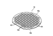
図1には、本発明に従って個々のチップに分離されるウエーハとしての半導体ウエーハの斜視図が示されている。図1に示す半導体ウエーハ10はシリコンウエーハからなっており、表面10aには複数の分割予定ライン101が格子状に形成されている。そして、半導体ウエーハ10の表面10aには、複数の分割予定ライン101によって区画された複数の領域にデバイス102が形成されている。以下、この半導体ウエーハ10を個々の半導体チップに分割する分割方法について説明する。
FIG. 1 shows a perspective view of a semiconductor wafer as a wafer separated into individual chips according to the present invention. A
半導体ウエーハ10を個々の半導体チップに分割するには、半導体ウエーハ10に対して透過性を有するパルスレーザー光線を複数の分割予定ライン101に沿って照射し、半導体ウエーハ10の内部に複数の分割予定ライン101に沿って変質層を形成することにより分割予定ラインに沿って強度を低下せしめる変質層形成工程を実施する。
この変質層形成工程は、図2に示すレーザー加工装置2を用いて実施する。図2に示すレーザー加工装置2は、被加工物を保持するチャックテーブル21と、該チャックテーブル21上に保持された被加工物にレーザー光線を照射するレーザー光線照射手段22と、チャックテーブル21上に保持された被加工物を撮像する撮像手段23を具備している。チャックテーブル21は、被加工物を吸引保持するように構成されており、図示しない加工送り手段によって図2において矢印Xで示す方向に加工送りされるとともに、図示しない割り出し送り手段によって図2において矢印Yで示す方向に割り出し送りされるようになっている。
In order to divide the semiconductor wafer 10 into individual semiconductor chips, a pulsed laser beam having transparency to the
This deteriorated layer forming step is performed using the
上記レーザー光線照射手段22は、実質上水平に配置された円筒形状のケーシング221の先端に装着された集光器222からパルスレーザー光線を照射する。また、上記レーザー光線照射手段12を構成するケーシング221の先端部に装着された撮像手段23は、図示の実施形態においては可視光線によって撮像する通常の撮像素子(CCD)の外に、被加工物に赤外線を照射する赤外線照明手段と、該赤外線照明手段によって照射された赤外線を捕らえる光学系と、該光学系によって捕らえられた赤外線に対応した電気信号を出力する撮像素子(赤外線CCD)等で構成されており、撮像した画像信号を後述する制御手段に送る。
The laser beam irradiation means 22 irradiates a pulsed laser beam from a
上述したレーザー加工装置1を用いて実施する変質層形成工程について、図2および図3を参照して説明する。
この変質層形成行程は、先ず上述した図2に示すレーザー加工装置2のチャックテーブル21上に半導体ウエーハ10を裏面10bを上にして載置し、該チャックテーブル21上に半導体ウエーハ10を吸着保持する。半導体ウエーハ10を吸引保持したチャックテーブル21は、図示しない加工送り手段によって撮像手段23の直下に位置付けられる。
The deteriorated layer forming step performed using the laser processing apparatus 1 described above will be described with reference to FIGS.
In this deteriorated layer forming process, first, the
チャックテーブル21が撮像手段23の直下に位置付けられると、撮像手段23および図示しない制御手段によって半導体ウエーハ10のレーザー加工すべき加工領域を検出するアライメント作業を実行する。即ち、撮像手段23および図示しない制御手段は、半導体ウエーハ10の所定方向に形成されている分割予定ライン101と、該分割予定ライン101に沿ってレーザー光線を照射するレーザー光線照射手段22の集光器222との位置合わせを行うためのパターンマッチング等の画像処理を実行し、レーザー光線照射位置のアライメントを遂行する。また、半導体ウエーハ10に形成されている複数の分割予定ライン101と直交する方向に形成されている複数の分割予定ライン101に対しても、同様にレーザー光線照射位置のアライメントが遂行される。このとき、半導体ウエーハ10の複数の分割予定ライン101が形成されている表面10aは下側に位置しているが、撮像手段23が上述したように赤外線照明手段と赤外線を捕らえる光学系および赤外線に対応した電気信号を出力する撮像素子(赤外線CCD)等で構成された撮像手段を備えているので、裏面10bから透かして分割予定ライン101を撮像することができる。
When the chuck table 21 is positioned directly below the image pickup means 23, an alignment operation for detecting a processing region to be laser processed of the
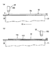
以上のようにしてチャックテーブル21上に保持された半導体ウエーハ10に形成されてい分割予定ライン101を検出し、レーザー光線照射位置のアライメントが行われたならば、図3の(a)で示すようにチャックテーブル21をレーザー光線照射手段22の集光器222が位置するレーザー光線照射領域に移動し、所定の分割予定ライン101の一端(図3の(a)において左端)をレーザー光線照射手段22の集光器222の直下に位置付ける。そして、集光器222から半導体ウエーハに対して透過性を有する波長のパルスレーザー光線を照射しつつチャックテーブル21を図3の(a)において矢印X1で示す方向に所定の加工送り速度で移動せしめる。そして、図3の(b)で示すようにレーザー光線照射手段22の集光器222の照射位置が分割予定ライン101の他端(図3の(b)において右端)の位置に達したら、パルスレーザー光線の照射を停止するとともにチャックテーブル21の移動を停止する。この変質層形成工程においては、パルスレーザー光線の集光点Pを半導体ウエーハ10の表面10a(下面)付近に合わせる。この結果、半導体ウエーハ10の表面10a(下面)に露出するとともに表面10aから内部に向けて変質層110が形成される。この変質層110は、溶融再固化層として形成される。
As shown in FIG. 3A, if the
上記変質層形成工程における加工条件は、例えば次のように設定されている。
光源 :LD励起QスイッチNd:YVO4スレーザー
波長 :1064nmのパルスレーザー
パルス出力 :10μJ
集光スポット径 :φ1μm
繰り返し周波数 :100kHz
加工送り速度 :100mm/秒
The processing conditions in the deteriorated layer forming step are set as follows, for example.
Light source: LD excitation Q switch Nd: YVO4 laser Laser wavelength: 1064 nm pulse laser Pulse output: 10 μJ
Condensing spot diameter: φ1μm
Repetition frequency: 100 kHz
Processing feed rate: 100 mm / sec
上記変質層110は、表面10aおよび裏面10bに露出しないように内部だけに形成してもよく、また、上記集光点Pを段階的に変えて上述したレーザー加工工程を複数回実行することにより、複数の変質層110を形成してもよい。そして、上述した変質層形成工程を半導体ウエーハ2に形成された全ての分割予定ライン101に沿って実施する。
The altered
上述した変質層形成工程によって半導体ウエーハ10の内部に複数の分割予定ライン101に沿って変質層110を形成したならば、分割予定ラインに沿って変質層が形成されたウエーハの裏面を環状のフレームに装着された保持テープに貼着するウエーハ支持工程を実施する。即ち、図4に示すように環状のフレーム3の内側開口部を覆うように外周部が装着された保持テープ30の表面に半導体ウエーハ10の裏面10bを貼着する。なお、上記保持テープ30は、図示の実施形態においては厚さが100μmのポリ塩化ビニル(PVC)からなるシート基材の表面にアクリル樹脂系の粘着剤が厚さが5μm程度塗布されている。
If the deteriorated
なお、ウエーハ支持工程は上記変質層形成工程の前に実施してもよく、この場合、環状のフレーム3に装着された保持テープ30の表面に半導体ウエーハ10の裏面10bを貼着した状態で上述した変質層形成工程を実施する。即ち、図5の(a)および(b)に示すように上記レーザー加工装置2のチャックテーブル21上に半導体ウエーハ10の保持テープ30側を載置する。そして、図示しない吸引手段を作動することにより、保持テープ30を介して半導体ウエーハ10をチャックテーブル21上に保持する。なお、図5の(a)および(b)においては保持テープ30が装着された環状のフレーム3を省いて示しているが、環状のフレーム3はチャックテーブル21に配設された適宜のフレーム保持手段に保持される。そして、上述したレーザー光線照射位置のアライメント作業が実施される。次に、図5の(a)に示すようにチャックテーブル21をレーザー光線照射手段22の集光器222が位置するレーザー光線照射領域に移動し、所定の分割予定ライン101の一端(図5の(a)において左端)をレーザー光線照射手段22の集光器222の直下に位置付ける。そして、集光器222から半導体ウエーハに対して透過性を有する波長のパルスレーザー光線を照射しつつチャックテーブル21を図5の(a)において矢印X1で示す方向に所定の加工送り速度で移動せしめる。そして、図5の(b)で示すようにレーザー光線照射手段22の集光器222の照射位置が分割予定ライン101の他端(図3の(b)において右端)の位置に達したら、パルスレーザー光線の照射を停止するとともにチャックテーブル21の移動を停止する。この変質層形成工程においては、パルスレーザー光線の集光点Pを半導体ウエーハ10の裏面10b(下面)付近に合わせる。この結果、半導体ウエーハ10の裏面10b(下面)に露出するとともに裏面10bから内部に向けて変質層110が形成される。
Note that the wafer support step may be performed before the above-described deteriorated layer forming step. In this case, the above-described process is performed with the
上述した変質層形成工程およびウエーハ支持工程を実施したならば、保持テープを介してウエーハを支持した環状のフレームをウエーハを下側にして保持した状態で、ウエーハに変質層が形成された分割予定ラインに沿って外力を付与し、ウエーハを分割予定ラインに沿って破断するウエーハ破断工程を実施する。このウエーハ破断工程は、図6および図7に示すウエーハの分割装置を用いて実施する。図6には本発明に従って構成された分割装置の一実施形態の斜視図が示されており、図7には図6に示す分割装置の分解斜視図が示されている。図6および図7に示すウエーハの分割装置4は、固定基台40と、該固定基台40の中央部上面に配設され上記環状のフレーム3を保持するフレーム保持手段5と、該フレーム保持手段5に保持された上記環状のフレーム3に装着された上記保持テープ30を挟持する複数(図示の実施形態においては4個)のテープ挟持手段6と、該複数のテープ挟持手段6をそれぞれ径方向に移動せしめる複数(図示の実施形態においては4個)のテープ拡張手段7とを具備している。
If the above-mentioned deteriorated layer forming step and wafer supporting step are performed, the divisional schedule in which the deteriorated layer is formed on the wafer with the annular frame supporting the wafer via the holding tape held with the wafer facing down A wafer breaking step is performed in which an external force is applied along the line and the wafer is broken along the line to be divided. This wafer breaking step is performed using the wafer dividing apparatus shown in FIGS. FIG. 6 shows a perspective view of an embodiment of a dividing apparatus constructed according to the present invention, and FIG. 7 shows an exploded perspective view of the dividing apparatus shown in FIG. 6 and 7 includes a fixed
上記固定基台40は円盤状に形成され、その上面には中心部を通って直角に交差する案内溝41、41が形成されている。また、固定基台40の上記案内溝41、41が形成された外周部は、外方に突出して形成されている。
The fixed
上記フレーム保持手段3は、固定基台40の上面に配設された4本の支持柱51と、該4本の支持柱51の上端に取り付けられた環状のフレーム保持部材52とからなっている。4本の支持柱51は、固定基台40に形成された案内溝41と41の間にそれぞれ配設されている。環状のフレーム保持部材42は、上記環状のフレーム3と略対応する大きさに形成されており、上面が環状のフレーム3を載置するための載置面521となっている。このフレーム保持部材52は、図7に示すように断面形状が逆L字状に形成されており、上記載置面521と平行な被支持面522と、外周側で垂下する規制部523を備えている。また、フレーム保持部材52には、外周には4個のクランプ53が周方向に互いに等角度をもって配設されている。このように構成されたフレーム保持部材52は、上記4本の支持柱51の上端面上に被支持面522を載置し、図示しない固定手段によって固定される。
The frame holding means 3 includes four
上記4個のテープ挟持手段6は、上記固定基台40に形成された案内溝41、41上に配設されている。即ち、4個のテープ挟持手段6は、周方向に互いに等角度をもって配設されている。このように配設されたテープ挟持手段6は、それぞれL字状に形成された可動基台61と、該可動基台61に上下方向に移動可能に装着された第1の挟持機構62および第2の挟持機構63と、該第1の挟持機構62および第2の挟持機構63をそれぞれ上下方向に移動せしめる第1の移動機構64および第2の移動機構65とを具備している。可動基台61は、移動部611と、該移動部611の上面から立設して形成された支持部612とからなっている。移動部611の下面には上記案内溝41に嵌合する被案内レール611aが設けられており、この被案内レール611aを案内溝41に嵌合することにより、可動基台61は円盤状の固定基盤40に案内溝41に沿って径方向に移動可能に構成される。また、移動部611には、雌ネジ611bが貫通して形成されている。上記支持部612の内側の面(互いに対向する側の面)には上下方向に延びる案内レール612aが設けられており、外側の面には上下方向に延びる長溝612bが形成されている。また、案内レール612aには、内側の面から上記長溝612bに達し上下方向に延びる長穴612cが形成されている。
The four tape clamping means 6 are disposed on
上記第1の挟持機構62は、上記可動基台61の支持部612に設けられた案内レール612aに沿って移動可能に配設された支持アーム621と、該支持アーム621に取り付けられた挟持部材622とからなっている。支持アーム621の基端には上記案内レール612aと嵌合する被案内溝621aが設けられており、この被案内溝621aを案内レール612aに嵌合することにより、支持アーム621は可動基台61の支持部612に案内レール612aに沿って上下方向に移動可能に構成される。また、支持アーム621の基部には雌ネジ631bを備えた雌ネジブロック631cが設けられており、この雌ネジブロック621cが上記長穴612cを挿通して配設される。上記挟持部材622は、上記半導体ウエーハ10の半径より僅かに大きい曲率半径を持って形成されており、その上端面(後述する第2の挟持機構63の挟持部材と対向する面)にはゴム等の摩擦係数の大きい摩擦部材623が装着されている。このように構成された挟持部材622の背面には取り付け部材624が固着されており、この取り付け部材624が支持アーム631の先端にネジ625によって着脱可能に取り付けられる。
The
上記第2の挟持機構63は、上記可動基台61の支持部612に設けられた案内レール612aに沿って移動可能に配設された支持アーム631と、該支持アーム631に取り付けられた挟持部材632とからなっている。支持アーム631の基端には上記案内レール612aと嵌合する被案内溝631aが設けられており、この被案内溝631aを案内レール612aに嵌合することにより、支持アーム631は可動基台61の支持部612に案内レール612aに沿って上下方向に移動可能に構成される。また、支持アーム631の基部には雌ネジ631bを備えた雌ネジブロック631cが設けられており、この雌ネジブロック631cが上記長穴612cを挿通して配設される。上記挟持部材632は、上記半導体ウエーハ10の半径より僅かに大きい曲率半径を持って形成されており、その下端面(上記第1の挟持機構62の挟持部材622と対向する面)には保持テープ30の表面に塗布された糊の付着を防止するためポリテトラフルオロエチレン等のブラスチック部材633が装着されている。このように構成された挟持部材632の背面には取り付け部材634が固着されており、この取り付け部材634が支持アーム631の先端にネジ635によって着脱可能に取り付けられる。
The
上記第1の挟持機構62を上下方向に移動せしめる第1の移動機構64は、上記可動基台61の支持部612に形成された長溝612b内に案内レール612aと平行に配設され上記支持アーム621の基部に設けられた雌ネジブロック621cの雌ネジ621bと螺合する雄ネジロッド641と、可動基台61の支持部612に配設され雄ネジロッド641の一端部を回転可能に支持する軸受642と、雄ネジロッド641の他端に連結され雄ネジロッド641を回転駆動するためのパルスモータ643とからなっている。このように構成された第1の移動機構64は、パルスモータ643を駆動して雄ネジロッド641を回動することにより、第1の挟持機構62を案内レール612aに沿って上下方向に移動せしめる。
The first moving
上記第2の挟持機構63を上下方向に移動せしめる第2の移動機構65は、上記第1の移動機構64と同様の構成で第1の移動機構64の上側に配設されている。即ち、第2の移動機構65は、上記可動基台41の支持部612に形成された長溝612b内に案内レール612aと平行に配設され上記支持アーム631の基部に設けられた雌ネジブロック631cの雌ネジ631bと螺合する雄ネジロッド651と、可動基台61の支持部612に配設され雄ネジロッド651の一端部を回転可能に支持する軸受652と、雄ネジロッド651の他端に連結され雄ネジロッド651を回転駆動するためのパルスモータ653とからなっている。このように構成された第2の移動機構65は、パルスモータ653を駆動して雄ネジロッド651を回動することにより、第2の挟持機構63を案内レール612aに沿って上下方向に移動せしめる。
The
上記4個のテープ挟持手段6をそれぞれ径方向に移動せしめる4個のテープ拡張手段7は、上記固定基台40の案内溝41、41に沿って配設されている。このテープ拡張手段7は、案内溝41と平行に配設され上記可動基台61の移動部611に形成された雌ネジ611bと螺合する雄ネジロッド71と、固定基台40に配設され雄ネジロッド71の一端部を回転可能に支持する軸受72と、雄ネジロッド71の他端と連結され雄ネジロッド71を回転駆動するためのパルスモータ73とからなっている。このように構成されたテープ拡張手段は、パルスモータ73を駆動して雄ネジロッド71を回動することにより、テープ挟持手段6をそれぞれ径方向に移動せしめる。
The four tape expanding means 7 for moving the four tape clamping means 6 in the radial direction are arranged along the
図示の実施形態におけるウエーハの分割装置4は、フレーム保持手段5に保持された環状のフレーム3に装着された保持テープ30に貼着されているウエーハの下方からイオン化されたエアーを供給してウエーハに帯電している静電気を除去する除電手段8を具備している。除電手段8は、イオン化したエアーを送出するイオン化エアー供給器81と、該イオン化エアー供給器81から送出されたイオン化したエアーを上記フレーム保持手段5に保持された環状のフレーム3に装着された保持テープ30に貼着されているウエーハに向けて噴出するイオン化エアー噴出管82とからなっている。
The wafer dividing device 4 in the illustrated embodiment supplies ionized air from below the wafer attached to the holding
図6および図7に示す実施形態におけるウエーハの分割装置4は以上のように構成されており、以下このウエーハの分割装置4を用いて実施するウエーハ破断工程について、図8および図9も参照して説明する。
上記図1、図4に示すように分割予定ライン101に沿って変質層110が形成された半導体ウエーハ10を保持テープ30を介して支持した環状のフレーム3を、図8の(a)に示すように半導体ウエーハ10を下側にして上記フレーム保持手段5を構成する環状のフレーム保持部材52の載置面521上に載置し、クランプ53によってフレーム保持部材52に固定する(ウエーハ支持工程)。このとき、テープ挟持手段6を構成する第1の挟持機構62および第2の挟持機構63は、図8の(a)に示す待機位置に位置付けられている。
The wafer dividing device 4 in the embodiment shown in FIG. 6 and FIG. 7 is configured as described above, and referring to FIG. 8 and FIG. 9 as well for the wafer breaking process to be performed using the wafer dividing device 4 hereinafter. I will explain.
An
半導体ウエーハ10を保持テープ30を介して支持した環状のフレーム3をフレーム保持部材52に保持したならば、テープ挟持手段6を構成する第1の挟持機構62および第2の挟持機構63を上下方向に移動する第1に移動機構64および第2の移動機構65を作動して、第1の挟持機構62を上方に作動するとともに第2の挟持機構63を下方に移動せしめる。この結果、図8の(b)に示すように互いに対向して配設された第1の挟持機構62を構成する挟持部材622に取り付けられた摩擦部材623と、第2の挟持機構63を構成する挟持部材632に取り付けられた摩擦部材633によって、保持テープ30における環状のフレーム3の内周と半導体ウエーハ10との間の領域を挟持する。そして、上記除電手段8のイオン化エアー供給器81を作動して、イオン化エアー噴出管82からイオン化されたエアーを半導体ウエーハ10の表面a(下面)に供給し、半導体ウエーハ10の表面aに帯電されている静電気を除去する。
If the
以上のようにして、4個のテープ挟持手段6によって保持テープ30を挟持したならば、上記テープ拡張手段7を作動して4個のテープ挟持手段6をそれぞれ径方向外方に移動する。従って、環状のフレーム3に装着された保持テープ30は、図9に示すように4個のテープ挟持手段6によって放射状に拡張される。このとき、図示の実施形態においては、保持テープ30は挟持部材622と632に取り付けられた摩擦部材623と633によって挟持されているので、テープ挟持手段6に作用する力を確実に保持テープ30に伝えることができる。この結果、保持テープ30に貼着されている半導体ウエーハ10には、放射状に引張力が作用する。このように半導体ウエーハ10に放射状に引張力が作用すると、各分割予定ライン101に沿って形成された変質層110は強度が低下せしめられているので、半導体ウエーハ10は変質層110に沿って破断され個々の半導体チップ100に分割される。なお、本発明者等の実験によると保持テープ30を5mm程度を引き伸ばしたときに半導体ウエーハ10を変質層110に沿って破断することができた。このように引き伸ばし量が少なくても分割することができるので、保持テープ30のたるみを低減できる。この後に、図示しないピックアップ手段のピックアップコレットによって半導体チップ100をピックアップし、図示しないトレーまたはダイボンディング工程に搬送する。
As described above, when the holding
上述したウエーハ破断工程においては、半導体ウエーハ10の表面10aを下側にして実施するので、半導体ウエーハ10が変質層110に沿って破断される際に飛散する微細な破片は自重で落下するため、半導体ウエーハ10の表面10aに形成されたデバイス102に付着することはない。また、上記実施形態においては、半導体ウエーハ10の表面10aにイオン化されたエアーが供給され半導体ウエーハ10の表面10aに帯電している静電気が除去されているので、半導体ウエーハ10が変質層110に沿って破断される際に飛散する微細な破片が静電気によってデバイス102に付着することもない。
In the above-described wafer breaking step, since the
2:レーザー加工装置
21:レーザー加工装置のチャックテーブル
22:レーザー光線照射手段
23:撮像手段
3:環状のフレーム
30:保持テープ
4:テープ拡張装置
40:固定基台
5:フレーム保持手段
51:支持柱
52:環状のフレーム保持部材
53:クランプ
6:テープ保持手段
61:可動基台
62:第1の挟持機構
621:支持アーム
622:挟持部材
623:摩擦部材
63:第2の挟持機構
631:支持アーム
632:挟持部材
633:摩擦部材
64:第1の移動機構
641:雄ネジロッド
643:パルスモータ
65:第2の移動機構
651:雄ネジロッド
653:パルスモータ
7:テープ拡張手段
71:雄ネジロッド
73:パルスモータ
8:除電手段
81:イオン化エアー供給器
82:イオン化エアー噴出管
10:半導体ウエーハ
100:半導体チップ
101:分割予定ライン
102:デバイス
110:変質層
2: Laser processing device 21: Chuck table of laser processing device 22: Laser beam irradiation means 23: Imaging means 3: Annular frame 30: Holding tape 4: Tape expansion device 40: Fixed base 5: Frame holding means 51: Support column 52: annular frame holding member 53: clamp 6: tape holding means 61: movable base 62: first clamping mechanism 621: support arm 622: clamping member 623: friction member 63: second clamping mechanism 631: support arm 632: clamping member 633: friction member 64: first moving mechanism 641: male screw rod 643: pulse motor 65: second moving mechanism 651: male screw rod 653: pulse motor 7: tape expansion means 71: male screw rod 73: pulse Motor 8: Static elimination means 81: Ionized air supply device 82: Ionized air Extraction pipe 10: semiconductor wafer 100: a semiconductor chip 101: dividing lines 102: Device 110: altered layer
Claims (4)
保持テープを介してウエーハを支持した環状のフレームをウエーハの表面を下側にして保持した状態で、ウエーハに変質層が形成された分割予定ラインに沿って外力を付与し、ウエーハを分割予定ラインに沿って破断する、
ことを特徴とするウエーハの分割方法。 A wafer in which a plurality of division lines are formed in a lattice pattern on the surface, a device is formed in a plurality of regions partitioned by the plurality of division lines, and a deteriorated layer is formed along the plurality of division lines inside Is a method for dividing a wafer that breaks along a plurality of division lines in a state where the back surface is attached to a holding tape attached to an annular frame,
With the annular frame supporting the wafer via the holding tape held with the wafer surface facing down, external force is applied along the planned division line where the altered layer is formed on the wafer, and the wafer is divided. Break along,
A wafer dividing method characterized by the above.
該環状のフレームを保持するフレーム保持手段と、
該フレーム保持手段に保持された環状のフレームに装着された保持テープを拡張するテープ拡張手段と、該フレーム保持手段に保持された環状のフレームに装着された保持テープに貼着されているウエーハの下方からイオン化されたエアーを供給し、ウエーハに帯電している静電気を除去する除電手段と、を具備している、
ことを特徴とするウエーハの分割装置。 A wafer in which a plurality of division lines are formed in a lattice pattern on the surface, a device is formed in a plurality of regions partitioned by the plurality of division lines, and a deteriorated layer is formed along the plurality of division lines inside In a wafer splitting device that breaks along a plurality of scheduled dividing lines in a state where the back surface is attached to a holding tape attached to an annular frame,
Frame holding means for holding the annular frame;
A tape expanding means for expanding a holding tape attached to an annular frame held by the frame holding means, and a wafer attached to the holding tape attached to the annular frame held by the frame holding means. A static elimination means for supplying ionized air from below and removing static electricity charged on the wafer,
A wafer dividing apparatus characterized by the above.
Priority Applications (2)
| Application Number | Priority Date | Filing Date | Title |
|---|---|---|---|
| JP2006130603A JP2007305687A (en) | 2006-05-09 | 2006-05-09 | Dicing method and dicing device of wafer |
| CN2007101028521A CN101071791B (en) | 2006-05-09 | 2007-05-09 | Cutting method of chip and apparatus |
Applications Claiming Priority (1)
| Application Number | Priority Date | Filing Date | Title |
|---|---|---|---|
| JP2006130603A JP2007305687A (en) | 2006-05-09 | 2006-05-09 | Dicing method and dicing device of wafer |
Publications (1)
| Publication Number | Publication Date |
|---|---|
| JP2007305687A true JP2007305687A (en) | 2007-11-22 |
Family
ID=38839391
Family Applications (1)
| Application Number | Title | Priority Date | Filing Date |
|---|---|---|---|
| JP2006130603A Pending JP2007305687A (en) | 2006-05-09 | 2006-05-09 | Dicing method and dicing device of wafer |
Country Status (2)
| Country | Link |
|---|---|
| JP (1) | JP2007305687A (en) |
| CN (1) | CN101071791B (en) |
Cited By (11)
| Publication number | Priority date | Publication date | Assignee | Title |
|---|---|---|---|---|
| JP2009177032A (en) * | 2008-01-25 | 2009-08-06 | Disco Abrasive Syst Ltd | Wafer carrier device and wafer machining device |
| JP2009272502A (en) * | 2008-05-09 | 2009-11-19 | Disco Abrasive Syst Ltd | Film-like adhesive fracturing apparatus and fracturing method |
| JP2011119549A (en) * | 2009-12-04 | 2011-06-16 | Lintec Corp | Adhesive sheet for stealth dicing, and method of manufacturing semiconductor device |
| JP2013041967A (en) * | 2011-08-15 | 2013-02-28 | Disco Abrasive Syst Ltd | Division device |
| JP2014143297A (en) * | 2013-01-24 | 2014-08-07 | Disco Abrasive Syst Ltd | Extension device and extension method |
| JP2014143313A (en) * | 2013-01-24 | 2014-08-07 | Disco Abrasive Syst Ltd | Extension device and extension method |
| JP2016081974A (en) * | 2014-10-10 | 2016-05-16 | リンテック株式会社 | Separation device and separation method |
| JP2018181921A (en) * | 2017-04-05 | 2018-11-15 | 株式会社ディスコ | Division device |
| CN108987302A (en) * | 2017-06-05 | 2018-12-11 | 株式会社迪思科 | Band expanding unit |
| JP2019067945A (en) * | 2017-10-02 | 2019-04-25 | 株式会社ディスコ | Tape expansion device and tape expansion method |
| JP7355618B2 (en) | 2018-12-04 | 2023-10-03 | 株式会社ディスコ | Wafer splitting device |
Families Citing this family (2)
| Publication number | Priority date | Publication date | Assignee | Title |
|---|---|---|---|---|
| JP5508133B2 (en) * | 2010-05-19 | 2014-05-28 | 株式会社ディスコ | Plate-shaped material dividing device |
| JP6111827B2 (en) * | 2013-04-30 | 2017-04-12 | 三星ダイヤモンド工業株式会社 | Break jig |
Citations (6)
| Publication number | Priority date | Publication date | Assignee | Title |
|---|---|---|---|---|
| JPS63260407A (en) * | 1987-04-17 | 1988-10-27 | 三菱電機株式会社 | Device and method of dividing semiconductor wafer |
| JPH0252705A (en) * | 1988-08-17 | 1990-02-22 | Nec Kyushu Ltd | Dividing method for semiconductor wafer |
| JPH08323737A (en) * | 1995-05-31 | 1996-12-10 | Nippondenso Co Ltd | Semiconductor wafer dividing apparatus |
| JPH09148276A (en) * | 1995-11-24 | 1997-06-06 | Tsukuba Seiko Kk | Wafer braking device |
| JPH1074712A (en) * | 1996-08-29 | 1998-03-17 | New Japan Radio Co Ltd | Wafer breaking device |
| JP2005294470A (en) * | 2004-03-31 | 2005-10-20 | Disco Abrasive Syst Ltd | Tape extension device |
Family Cites Families (2)
| Publication number | Priority date | Publication date | Assignee | Title |
|---|---|---|---|---|
| JP4659300B2 (en) * | 2000-09-13 | 2011-03-30 | 浜松ホトニクス株式会社 | Laser processing method and semiconductor chip manufacturing method |
| CN100428418C (en) * | 2004-02-09 | 2008-10-22 | 株式会社迪斯科 | Method for cutting wafer |
-
2006
- 2006-05-09 JP JP2006130603A patent/JP2007305687A/en active Pending
-
2007
- 2007-05-09 CN CN2007101028521A patent/CN101071791B/en active Active
Patent Citations (6)
| Publication number | Priority date | Publication date | Assignee | Title |
|---|---|---|---|---|
| JPS63260407A (en) * | 1987-04-17 | 1988-10-27 | 三菱電機株式会社 | Device and method of dividing semiconductor wafer |
| JPH0252705A (en) * | 1988-08-17 | 1990-02-22 | Nec Kyushu Ltd | Dividing method for semiconductor wafer |
| JPH08323737A (en) * | 1995-05-31 | 1996-12-10 | Nippondenso Co Ltd | Semiconductor wafer dividing apparatus |
| JPH09148276A (en) * | 1995-11-24 | 1997-06-06 | Tsukuba Seiko Kk | Wafer braking device |
| JPH1074712A (en) * | 1996-08-29 | 1998-03-17 | New Japan Radio Co Ltd | Wafer breaking device |
| JP2005294470A (en) * | 2004-03-31 | 2005-10-20 | Disco Abrasive Syst Ltd | Tape extension device |
Cited By (13)
| Publication number | Priority date | Publication date | Assignee | Title |
|---|---|---|---|---|
| JP2009177032A (en) * | 2008-01-25 | 2009-08-06 | Disco Abrasive Syst Ltd | Wafer carrier device and wafer machining device |
| JP2009272502A (en) * | 2008-05-09 | 2009-11-19 | Disco Abrasive Syst Ltd | Film-like adhesive fracturing apparatus and fracturing method |
| JP2011119549A (en) * | 2009-12-04 | 2011-06-16 | Lintec Corp | Adhesive sheet for stealth dicing, and method of manufacturing semiconductor device |
| JP2013041967A (en) * | 2011-08-15 | 2013-02-28 | Disco Abrasive Syst Ltd | Division device |
| JP2014143297A (en) * | 2013-01-24 | 2014-08-07 | Disco Abrasive Syst Ltd | Extension device and extension method |
| JP2014143313A (en) * | 2013-01-24 | 2014-08-07 | Disco Abrasive Syst Ltd | Extension device and extension method |
| JP2016081974A (en) * | 2014-10-10 | 2016-05-16 | リンテック株式会社 | Separation device and separation method |
| JP2018181921A (en) * | 2017-04-05 | 2018-11-15 | 株式会社ディスコ | Division device |
| CN108987302A (en) * | 2017-06-05 | 2018-12-11 | 株式会社迪思科 | Band expanding unit |
| JP2018206947A (en) * | 2017-06-05 | 2018-12-27 | 株式会社ディスコ | Tape extension device |
| JP2019067945A (en) * | 2017-10-02 | 2019-04-25 | 株式会社ディスコ | Tape expansion device and tape expansion method |
| JP7030469B2 (en) | 2017-10-02 | 2022-03-07 | 株式会社ディスコ | Tape expansion device and tape expansion method |
| JP7355618B2 (en) | 2018-12-04 | 2023-10-03 | 株式会社ディスコ | Wafer splitting device |
Also Published As
| Publication number | Publication date |
|---|---|
| CN101071791A (en) | 2007-11-14 |
| CN101071791B (en) | 2012-04-25 |
Similar Documents
| Publication | Publication Date | Title |
|---|---|---|
| JP2007305687A (en) | Dicing method and dicing device of wafer | |
| JP5307612B2 (en) | Processing method of optical device wafer | |
| US7507639B2 (en) | Wafer dividing method | |
| KR102272434B1 (en) | Wafer processing method | |
| JP5436917B2 (en) | Laser processing equipment | |
| JP4342992B2 (en) | Laser processing machine chuck table | |
| US20050282359A1 (en) | Wafer processing method | |
| KR20160072775A (en) | Method of machining wafer | |
| JP4630689B2 (en) | Wafer division method | |
| US20070045799A1 (en) | Wafer processing method and adhesive tape used in the wafer processing method | |
| TWI618132B (en) | Optical component wafer processing method | |
| JP2008294191A (en) | Wafer dividing method | |
| JP2007173475A (en) | Method for dividing wafer | |
| JP2013008831A (en) | Processing method of wafer | |
| US20080293220A1 (en) | Wafer dividing method | |
| JP2007059829A (en) | Machining method of wafer, and pressure-sensitive adhesive tape used for the same | |
| JP4684569B2 (en) | Tape expansion unit | |
| JP4447392B2 (en) | Wafer dividing method and dividing apparatus | |
| JP2011091293A (en) | Method for processing wafer | |
| JP4833657B2 (en) | Wafer division method | |
| JP2006108273A (en) | Method and apparatus of dividing wafer | |
| KR20170049397A (en) | Wafer processing method | |
| JP2010021397A (en) | Method of cleaning wafer | |
| US10692766B2 (en) | Method of cutting workpiece | |
| JP2008311404A (en) | Working method of wafer |
Legal Events
| Date | Code | Title | Description |
|---|---|---|---|
| A621 | Written request for application examination |
Free format text: JAPANESE INTERMEDIATE CODE: A621 Effective date: 20090417 |
|
| A977 | Report on retrieval |
Free format text: JAPANESE INTERMEDIATE CODE: A971007 Effective date: 20110414 |
|
| A131 | Notification of reasons for refusal |
Effective date: 20110419 Free format text: JAPANESE INTERMEDIATE CODE: A131 |
|
| A521 | Written amendment |
Effective date: 20110616 Free format text: JAPANESE INTERMEDIATE CODE: A523 |
|
| A131 | Notification of reasons for refusal |
Effective date: 20110712 Free format text: JAPANESE INTERMEDIATE CODE: A131 |
|
| A521 | Written amendment |
Effective date: 20110905 Free format text: JAPANESE INTERMEDIATE CODE: A523 |
|
| A02 | Decision of refusal |
Effective date: 20111101 Free format text: JAPANESE INTERMEDIATE CODE: A02 |