JP2007214267A - Semiconductor device - Google Patents
Semiconductor device Download PDFInfo
- Publication number
- JP2007214267A JP2007214267A JP2006031210A JP2006031210A JP2007214267A JP 2007214267 A JP2007214267 A JP 2007214267A JP 2006031210 A JP2006031210 A JP 2006031210A JP 2006031210 A JP2006031210 A JP 2006031210A JP 2007214267 A JP2007214267 A JP 2007214267A
- Authority
- JP
- Japan
- Prior art keywords
- type
- semiconductor device
- drain
- region
- type source
- Prior art date
- Legal status (The legal status is an assumption and is not a legal conclusion. Google has not performed a legal analysis and makes no representation as to the accuracy of the status listed.)
- Withdrawn
Links
- 239000004065 semiconductor Substances 0.000 title claims description 34
- 238000009792 diffusion process Methods 0.000 claims abstract description 37
- 239000010410 layer Substances 0.000 claims description 38
- 239000000758 substrate Substances 0.000 claims description 12
- 239000012535 impurity Substances 0.000 claims description 9
- OAICVXFJPJFONN-UHFFFAOYSA-N Phosphorus Chemical compound [P] OAICVXFJPJFONN-UHFFFAOYSA-N 0.000 claims description 8
- 229910052698 phosphorus Inorganic materials 0.000 claims description 8
- 239000011574 phosphorus Substances 0.000 claims description 8
- 239000011229 interlayer Substances 0.000 claims description 6
- 229910052785 arsenic Inorganic materials 0.000 claims description 4
- RQNWIZPPADIBDY-UHFFFAOYSA-N arsenic atom Chemical compound [As] RQNWIZPPADIBDY-UHFFFAOYSA-N 0.000 claims description 4
- 230000015556 catabolic process Effects 0.000 description 8
- XUIMIQQOPSSXEZ-UHFFFAOYSA-N Silicon Chemical compound [Si] XUIMIQQOPSSXEZ-UHFFFAOYSA-N 0.000 description 5
- 229910052710 silicon Inorganic materials 0.000 description 5
- 239000010703 silicon Substances 0.000 description 5
- 229910021420 polycrystalline silicon Inorganic materials 0.000 description 3
- 230000005611 electricity Effects 0.000 description 2
- 230000003068 static effect Effects 0.000 description 2
- ZOXJGFHDIHLPTG-UHFFFAOYSA-N Boron Chemical compound [B] ZOXJGFHDIHLPTG-UHFFFAOYSA-N 0.000 description 1
- 229910052796 boron Inorganic materials 0.000 description 1
- 230000000694 effects Effects 0.000 description 1
- 230000020169 heat generation Effects 0.000 description 1
- 150000002500 ions Chemical class 0.000 description 1
- 238000002955 isolation Methods 0.000 description 1
Images


Classifications
-
- H—ELECTRICITY
- H01—ELECTRIC ELEMENTS
- H01L—SEMICONDUCTOR DEVICES NOT COVERED BY CLASS H10
- H01L27/00—Devices consisting of a plurality of semiconductor or other solid-state components formed in or on a common substrate
- H01L27/02—Devices consisting of a plurality of semiconductor or other solid-state components formed in or on a common substrate including semiconductor components specially adapted for rectifying, oscillating, amplifying or switching and having potential barriers; including integrated passive circuit elements having potential barriers
- H01L27/04—Devices consisting of a plurality of semiconductor or other solid-state components formed in or on a common substrate including semiconductor components specially adapted for rectifying, oscillating, amplifying or switching and having potential barriers; including integrated passive circuit elements having potential barriers the substrate being a semiconductor body
-
- H—ELECTRICITY
- H01—ELECTRIC ELEMENTS
- H01L—SEMICONDUCTOR DEVICES NOT COVERED BY CLASS H10
- H01L29/00—Semiconductor devices specially adapted for rectifying, amplifying, oscillating or switching and having potential barriers; Capacitors or resistors having potential barriers, e.g. a PN-junction depletion layer or carrier concentration layer; Details of semiconductor bodies or of electrodes thereof ; Multistep manufacturing processes therefor
- H01L29/02—Semiconductor bodies ; Multistep manufacturing processes therefor
- H01L29/06—Semiconductor bodies ; Multistep manufacturing processes therefor characterised by their shape; characterised by the shapes, relative sizes, or dispositions of the semiconductor regions ; characterised by the concentration or distribution of impurities within semiconductor regions
- H01L29/10—Semiconductor bodies ; Multistep manufacturing processes therefor characterised by their shape; characterised by the shapes, relative sizes, or dispositions of the semiconductor regions ; characterised by the concentration or distribution of impurities within semiconductor regions with semiconductor regions connected to an electrode not carrying current to be rectified, amplified or switched and such electrode being part of a semiconductor device which comprises three or more electrodes
- H01L29/107—Substrate region of field-effect devices
- H01L29/1075—Substrate region of field-effect devices of field-effect transistors
- H01L29/1079—Substrate region of field-effect devices of field-effect transistors with insulated gate
- H01L29/1083—Substrate region of field-effect devices of field-effect transistors with insulated gate with an inactive supplementary region, e.g. for preventing punch-through, improving capacity effect or leakage current
-
- H—ELECTRICITY
- H01—ELECTRIC ELEMENTS
- H01L—SEMICONDUCTOR DEVICES NOT COVERED BY CLASS H10
- H01L27/00—Devices consisting of a plurality of semiconductor or other solid-state components formed in or on a common substrate
- H01L27/02—Devices consisting of a plurality of semiconductor or other solid-state components formed in or on a common substrate including semiconductor components specially adapted for rectifying, oscillating, amplifying or switching and having potential barriers; including integrated passive circuit elements having potential barriers
- H01L27/0203—Particular design considerations for integrated circuits
- H01L27/0248—Particular design considerations for integrated circuits for electrical or thermal protection, e.g. electrostatic discharge [ESD] protection
- H01L27/0251—Particular design considerations for integrated circuits for electrical or thermal protection, e.g. electrostatic discharge [ESD] protection for MOS devices
- H01L27/0266—Particular design considerations for integrated circuits for electrical or thermal protection, e.g. electrostatic discharge [ESD] protection for MOS devices using field effect transistors as protective elements
-
- H—ELECTRICITY
- H01—ELECTRIC ELEMENTS
- H01L—SEMICONDUCTOR DEVICES NOT COVERED BY CLASS H10
- H01L29/00—Semiconductor devices specially adapted for rectifying, amplifying, oscillating or switching and having potential barriers; Capacitors or resistors having potential barriers, e.g. a PN-junction depletion layer or carrier concentration layer; Details of semiconductor bodies or of electrodes thereof ; Multistep manufacturing processes therefor
- H01L29/02—Semiconductor bodies ; Multistep manufacturing processes therefor
- H01L29/06—Semiconductor bodies ; Multistep manufacturing processes therefor characterised by their shape; characterised by the shapes, relative sizes, or dispositions of the semiconductor regions ; characterised by the concentration or distribution of impurities within semiconductor regions
- H01L29/10—Semiconductor bodies ; Multistep manufacturing processes therefor characterised by their shape; characterised by the shapes, relative sizes, or dispositions of the semiconductor regions ; characterised by the concentration or distribution of impurities within semiconductor regions with semiconductor regions connected to an electrode not carrying current to be rectified, amplified or switched and such electrode being part of a semiconductor device which comprises three or more electrodes
- H01L29/1025—Channel region of field-effect devices
- H01L29/1029—Channel region of field-effect devices of field-effect transistors
- H01L29/1033—Channel region of field-effect devices of field-effect transistors with insulated gate, e.g. characterised by the length, the width, the geometric contour or the doping structure
- H01L29/1041—Channel region of field-effect devices of field-effect transistors with insulated gate, e.g. characterised by the length, the width, the geometric contour or the doping structure with a non-uniform doping structure in the channel region surface
- H01L29/1045—Channel region of field-effect devices of field-effect transistors with insulated gate, e.g. characterised by the length, the width, the geometric contour or the doping structure with a non-uniform doping structure in the channel region surface the doping structure being parallel to the channel length, e.g. DMOS like
-
- H—ELECTRICITY
- H01—ELECTRIC ELEMENTS
- H01L—SEMICONDUCTOR DEVICES NOT COVERED BY CLASS H10
- H01L29/00—Semiconductor devices specially adapted for rectifying, amplifying, oscillating or switching and having potential barriers; Capacitors or resistors having potential barriers, e.g. a PN-junction depletion layer or carrier concentration layer; Details of semiconductor bodies or of electrodes thereof ; Multistep manufacturing processes therefor
- H01L29/02—Semiconductor bodies ; Multistep manufacturing processes therefor
- H01L29/06—Semiconductor bodies ; Multistep manufacturing processes therefor characterised by their shape; characterised by the shapes, relative sizes, or dispositions of the semiconductor regions ; characterised by the concentration or distribution of impurities within semiconductor regions
- H01L29/10—Semiconductor bodies ; Multistep manufacturing processes therefor characterised by their shape; characterised by the shapes, relative sizes, or dispositions of the semiconductor regions ; characterised by the concentration or distribution of impurities within semiconductor regions with semiconductor regions connected to an electrode not carrying current to be rectified, amplified or switched and such electrode being part of a semiconductor device which comprises three or more electrodes
- H01L29/1025—Channel region of field-effect devices
- H01L29/1029—Channel region of field-effect devices of field-effect transistors
- H01L29/1033—Channel region of field-effect devices of field-effect transistors with insulated gate, e.g. characterised by the length, the width, the geometric contour or the doping structure
- H01L29/105—Channel region of field-effect devices of field-effect transistors with insulated gate, e.g. characterised by the length, the width, the geometric contour or the doping structure with vertical doping variation
-
- H—ELECTRICITY
- H01—ELECTRIC ELEMENTS
- H01L—SEMICONDUCTOR DEVICES NOT COVERED BY CLASS H10
- H01L29/00—Semiconductor devices specially adapted for rectifying, amplifying, oscillating or switching and having potential barriers; Capacitors or resistors having potential barriers, e.g. a PN-junction depletion layer or carrier concentration layer; Details of semiconductor bodies or of electrodes thereof ; Multistep manufacturing processes therefor
- H01L29/66—Types of semiconductor device ; Multistep manufacturing processes therefor
- H01L29/86—Types of semiconductor device ; Multistep manufacturing processes therefor controllable only by variation of the electric current supplied, or only the electric potential applied, to one or more of the electrodes carrying the current to be rectified, amplified, oscillated or switched
- H01L29/861—Diodes
-
- H—ELECTRICITY
- H01—ELECTRIC ELEMENTS
- H01L—SEMICONDUCTOR DEVICES NOT COVERED BY CLASS H10
- H01L29/00—Semiconductor devices specially adapted for rectifying, amplifying, oscillating or switching and having potential barriers; Capacitors or resistors having potential barriers, e.g. a PN-junction depletion layer or carrier concentration layer; Details of semiconductor bodies or of electrodes thereof ; Multistep manufacturing processes therefor
- H01L29/02—Semiconductor bodies ; Multistep manufacturing processes therefor
- H01L29/06—Semiconductor bodies ; Multistep manufacturing processes therefor characterised by their shape; characterised by the shapes, relative sizes, or dispositions of the semiconductor regions ; characterised by the concentration or distribution of impurities within semiconductor regions
- H01L29/0603—Semiconductor bodies ; Multistep manufacturing processes therefor characterised by their shape; characterised by the shapes, relative sizes, or dispositions of the semiconductor regions ; characterised by the concentration or distribution of impurities within semiconductor regions characterised by particular constructional design considerations, e.g. for preventing surface leakage, for controlling electric field concentration or for internal isolations regions
- H01L29/0607—Semiconductor bodies ; Multistep manufacturing processes therefor characterised by their shape; characterised by the shapes, relative sizes, or dispositions of the semiconductor regions ; characterised by the concentration or distribution of impurities within semiconductor regions characterised by particular constructional design considerations, e.g. for preventing surface leakage, for controlling electric field concentration or for internal isolations regions for preventing surface leakage or controlling electric field concentration
- H01L29/0638—Semiconductor bodies ; Multistep manufacturing processes therefor characterised by their shape; characterised by the shapes, relative sizes, or dispositions of the semiconductor regions ; characterised by the concentration or distribution of impurities within semiconductor regions characterised by particular constructional design considerations, e.g. for preventing surface leakage, for controlling electric field concentration or for internal isolations regions for preventing surface leakage or controlling electric field concentration for preventing surface leakage due to surface inversion layer, e.g. with channel stopper
Landscapes
- Engineering & Computer Science (AREA)
- Power Engineering (AREA)
- Microelectronics & Electronic Packaging (AREA)
- Physics & Mathematics (AREA)
- Condensed Matter Physics & Semiconductors (AREA)
- General Physics & Mathematics (AREA)
- Computer Hardware Design (AREA)
- Ceramic Engineering (AREA)
- Semiconductor Integrated Circuits (AREA)
- Metal-Oxide And Bipolar Metal-Oxide Semiconductor Integrated Circuits (AREA)
- Insulated Gate Type Field-Effect Transistor (AREA)
Abstract
Description
本発明は半導体装置、特にCMOS半導体装置の静電気による破壊を防止するために用いられる半導体装置に関する。 The present invention relates to a semiconductor device, and more particularly to a semiconductor device used for preventing breakdown of a CMOS semiconductor device due to static electricity.
従来、CMOS半導体装置では、静電放電(Electrostatic discharge:以下ESDと称す)保護素子として、図3に示すようなゲートを基板電位におとしたコンベンショナル型のドレイン構造を持つNMOSトランジスタがよく用いられている。CMOS半導体装置の最大動作電圧以上でかつ通常のNMOSトランジスタではブレークダウンには至らない電圧範囲にておきるこのトランジスタの表面ブレークダウンを利用して、ドレイン103bとP型基板101の間に電流を流すことでP型基板101の電位の上昇を引き起こし、エミッタとなるソース103aとベースとなるP型基板101の間に順方向電圧がかかることにより、NPNバイポーラ動作をスイッチングさせ、大電荷を放出させるのが動作原理である。また、NMOSトランジスタのチャネルの長さであるL長を調節することにより、NPNバイポーラ動作時の保持電圧を半導体装置の最大動作電圧以上に容易に設定することが可能であり、全ての電荷を放出し終わった後、定常状態に復帰することができる。NMOSトランジスタのブレークダウン時に最も熱が発生するドレイン側N+層の構造はESD保護素子の電流耐性(熱耐性)を決める重要な因子である。発熱を分散させる構造、すなわちより深く均一なプロファイルが得られるリンがN+拡散層の不純物として一般的に用いられる。
しかしながら、半導体の微細化、デバイスの小型化が進められ、CMOS半導体装置の低電圧化及びゲート酸化膜の薄膜化により、従来のコンベンショナル型のドレイン構造を持つNMOSトランジスタを用いた静電保護回路では、表面ブレークダウンに至る前にゲート酸化膜破壊電圧に達してしまったり、静電保護回路が動作する前にCMOS半導体装置が静電気により破壊してしまったりするという問題点を有していた。 However, with the miniaturization of the semiconductor and the miniaturization of the device, the conventional electrostatic protection circuit using the NMOS transistor having the conventional drain structure has been reduced by reducing the voltage of the CMOS semiconductor device and reducing the thickness of the gate oxide film. The gate oxide breakdown voltage has been reached before the surface breakdown, or the CMOS semiconductor device has been destroyed by static electricity before the electrostatic protection circuit operates.
本発明は、従来のコンベンショナル型のドレイン構造を持つNMOSトランジスタを用いた静電保護回路では不可能であった動作電圧(トリガ電圧)および保持電圧が低く、かつ、自由に設定できる静電保護素子を、小さな占有面積でコストをかけずに提供することを目的とする。 The present invention provides an electrostatic protection element that has a low operating voltage (trigger voltage) and holding voltage, and that can be freely set, which is impossible with a conventional electrostatic protection circuit using an NMOS transistor having a conventional drain structure. The purpose is to provide a small occupying area without cost.
上記目的を達成するために本発明の半導体装置が採用した手段は次の通りである。
(1)P型半導体基板上に形成されたP型ウエル領域と、前記P型ウエル領域上に形成されたフィールド酸化膜と、前記P型ウエル領域上にゲート酸化膜を介して形成されたゲート電極と、前記フィールド酸化膜と前記ゲート電極とに囲まれているN型ソース・ドレイン領域と、前記N型ソース・ドレイン領域の間に局所的に形成されたP型ウェル領域よりも高濃度のP型領域と、前記ゲート電極と前記N型ソース・ドレインとそれらの上層に形成される配線とを電気的に絶縁する層間膜と、前記配線と前記ゲート電極と前記N型ソース・ドレインとを電気的に接続を行うためのコンタクト孔からなる半導体装置とした。
(2)前記N型ソース・ドレイン領域の間、全面にP型領域を形成した半導体装置とした。
(3)前記N型ソース・ドレイン領域の間に形成されたP型領域に導入する不純物濃度を1E16〜1E20atoms/cm3とした半導体装置とした。
(4)前記N型ソース・ドレイン領域に導入する不純物がリンである半導体装置とした。
(5)前記N型ソース・ドレイン領域に導入する不純物はリンと砒素とし、二重拡散構造にした半導体装置とした。
The means employed by the semiconductor device of the present invention to achieve the above object are as follows.
(1) A P-type well region formed on a P-type semiconductor substrate, a field oxide film formed on the P-type well region, and a gate formed on the P-type well region via a gate oxide film An N-type source / drain region surrounded by the electrode, the field oxide film and the gate electrode, and a higher concentration than the P-type well region locally formed between the N-type source / drain region. An interlayer film that electrically insulates a P-type region, the gate electrode, the N-type source / drain, and a wiring formed thereon, and the wiring, the gate electrode, and the N-type source / drain; A semiconductor device having contact holes for electrical connection was obtained.
(2) The semiconductor device has a P-type region formed on the entire surface between the N-type source / drain regions.
(3) The semiconductor device has an impurity concentration of 1E16 to 1E20 atoms / cm 3 introduced into a P-type region formed between the N-type source / drain regions.
(4) A semiconductor device in which the impurity introduced into the N-type source / drain region is phosphorus.
(5) Impurities to be introduced into the N-type source / drain regions are phosphorus and arsenic to form a semiconductor device having a double diffusion structure.
本発明によれば、コンベンショナル型のドレイン構造を持つNMOSトランジスタを用いた静電保護回路に、P型の不純物を導入することで、従来のコンベンショナル型のドレイン構造を持つNMOSトランジスタを用いた静電保護回路では不可能であったトリガ電圧は低くて、保持電圧が容易に設定可能な素子を得ることができる。これにより、低電圧化したCMOSトランジスタをESDから保護可能なESD保護回路を実現する事が出来、多くのICにおいて多大な効果が得られる。 According to the present invention, an electrostatic protection circuit using a conventional NMOS transistor having a conventional drain structure is introduced by introducing a P-type impurity into an electrostatic protection circuit using an NMOS transistor having a conventional drain structure. The trigger voltage, which is impossible with the protection circuit, is low, and an element in which the holding voltage can be easily set can be obtained. As a result, an ESD protection circuit capable of protecting a low-voltage CMOS transistor from ESD can be realized, and a great effect can be obtained in many ICs.
以下、図面を参照して本発明の好適な実施例を説明する。 Hereinafter, preferred embodiments of the present invention will be described with reference to the drawings.
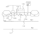
図1は本発明による半導体装置のコンベンショナル型のドレイン構造を持つNMOSトランジスタの第一実施例を示す模式的断面図である。 FIG. 1 is a schematic cross-sectional view showing a first embodiment of an NMOS transistor having a conventional drain structure of a semiconductor device according to the present invention.
P型シリコン半導体基板101上にP型ウェル領域102をつくり、P型ウェル領域上に形成するゲート酸化膜106及び多結晶シリコンゲート電極105と、ゲート電極両端のシリコン基板表面に形成する高濃度のN型ソース拡散層103aとN型ドレイン拡散層103bとの間に局所的に形成される高濃度のP型拡散層104及び前記P型ウェル領域102の電位を取るための高濃度のP型拡散層107から構成する。N型ドレイン拡散層103bは入出力端子への配線に接続され、N型ソース拡散層103aとP型ウェル領域102の電位を取るためのP型拡散層107及び多結晶シリコンゲート電極は基準電位であるVss配線に接続される。また、配線とゲート電極とN型ソース・ドレインとを電気的に接続を行うためのコンタクト孔(図示せず)を堆積された層間絶縁膜(図示せず)に形成する。素子の間に分離を目的としてフィールド酸化膜108及びチャネルストップ領域109が形成される。尚、必ずしもP型シリコン半導体基板を用いる必要はなく、N型シリコン半導体基板を用いて、NMOSトランジスタを作ってもよい。
A P-
入出力端子にプラス電荷が入ってきた場合、N型ドレイン拡散層103bとN型ソース・ドレイン拡散層の間に形成されたP型拡散層104のN+Pダイオードがブレークダウンし、これがトリガ電圧となり、P型ウェル層102内に電流が流れ、N型ドレイン拡散層〜P型ウェル層〜N型ソース拡散層からなるNPNトランジスタのバイポーラ動作をオンさせ、すばやく電荷を放出できる構造となっている。N型ドレイン拡散層及びP型拡散層の濃度を変えることにより容易にトリガ電圧を最大定格以上でゲート酸化膜破壊電圧以下に設定できる。P型拡散層を形成するためには、BF2またはボロンをドーズ量1×10¹²〜1×10¹⁶atoms/cm2でイオン注入する。これは濃度に換算すると1×1016〜1×1020atoms/cm3程度である。また、N型ソース拡散層とN型ドレイン拡散層の間にP型拡散層を形成することにより、パンチスルーを抑制することができ、L長を縮小することができる。
When a positive charge enters the input / output terminal, the N + P diode of the P-
また、図1で示したように、N型ソース拡散層とゲート直下に形成されたP型拡散層との距離(D1)を変更することにより容易にNPNトランジスタのバイポーラ動作の保持電圧を任意の値に設定することができる。更に、P型拡散層の濃度を変更することにより、容易に保持電圧を任意の値に設定することもできる。 In addition, as shown in FIG. 1, by changing the distance (D1) between the N-type source diffusion layer and the P-type diffusion layer formed immediately below the gate, the holding voltage for the bipolar operation of the NPN transistor can be easily set to an arbitrary value. Can be set to a value. Furthermore, the holding voltage can be easily set to an arbitrary value by changing the concentration of the P-type diffusion layer.
N型ドレイン拡散層はN+Pダイオードのブレークダウン時にもっとも熱が発生するので、深く均一な濃度プロファイルが得られるリンを使用し、発熱を分散させる構造となっている。これにより、ESD保護素子の熱耐性を向上することができる。さらに、N型ソース・ドレイン拡散層を形成する際に導入する不純物をリン・砒素の二重拡散層としてもよい。砒素を注入することにより、N+Pダイオードのブレークダウン耐圧を容易に下げることができる。 The N-type drain diffusion layer generates the most heat when the N + P diode breaks down. Therefore, the N-type drain diffusion layer has a structure in which the heat generation is dispersed by using phosphorus that provides a deep and uniform concentration profile. Thereby, the heat tolerance of an ESD protection element can be improved. Further, the impurity introduced when forming the N-type source / drain diffusion layer may be a double diffusion layer of phosphorus / arsenic. By implanting arsenic, the breakdown voltage of the N + P diode can be easily lowered.
また、ゲート電極をVSSに配線しておくことにより、リーク電流を抑制することができる構造となっている。ただし、ゲート電極は必ずしもつける必要はない。 Further, by previously connecting the gate electrode to V SS, and has a structure that can suppress leakage current. However, the gate electrode is not necessarily provided.
図2は本発明による半導体装置のコンベンショナル型のドレイン構造を持つNMOSトランジスタの第2実施例を示す模式的断面図である。 FIG. 2 is a schematic sectional view showing a second embodiment of the NMOS transistor having the conventional drain structure of the semiconductor device according to the present invention.
図2で示したように、N型ソース・ドレイン拡散層間のゲート直下全面にP型拡散層を形成してもよい。 As shown in FIG. 2, a P-type diffusion layer may be formed on the entire surface immediately below the gate between the N-type source / drain diffusion layers.
101 P型シリコン半導体基板
102 P型ウェル層
103a N+型ソース拡散層
103b N+型ドレイン拡散層
104 P型拡散層
105 多結晶シリコンゲート電極
106 ゲート酸化膜
107 P+型拡散層
108 フィールド酸化膜
109 チャネルストップ
101 P type silicon semiconductor substrate 102 P type well layer 103a N + type
Claims (7)
前記P型ウエル領域上に形成され、内部に能動素子領域を有するフィールド酸化膜と、
前記P型ウエル領域上にゲート酸化膜を介して形成されたゲート電極と、
前記フィールド酸化膜と前記ゲート電極とに囲まれているN型ソースおよびドレイン領域と、
前記ドレイン領域に接して、前記N型ソースおよびドレイン領域の間に形成された前記P型ウェル領域よりも高濃度のP型領域と、
前記N型ソースおよびドレイン領域と前記ゲート電極の上層に形成される配線とを電気的に絶縁する層間絶縁膜と
前記配線と前記ゲート電極と前記N型ソースおよびドレインとをそれぞれ電気的に接続するため前記層間絶縁膜に設けられたコンタクト孔とからなる半導体装置。 A P-type well region formed on a P-type semiconductor substrate;
A field oxide film formed on the P-type well region and having an active element region therein;
A gate electrode formed on the P-type well region via a gate oxide film;
N-type source and drain regions surrounded by the field oxide film and the gate electrode;
A P-type region having a higher concentration than the P-type well region formed between the N-type source and drain regions in contact with the drain region;
An interlayer insulating film that electrically insulates the N-type source and drain regions and a wiring formed in an upper layer of the gate electrode, and the wiring, the gate electrode, and the N-type source and drain are electrically connected to each other. Therefore, a semiconductor device comprising a contact hole provided in the interlayer insulating film.
前記P型ウエル領域上に形成され、内部に能動素子領域を有するフィールド酸化膜と、
前記P型ウエル領域上にゲート酸化膜を介して形成されたゲート電極と、
前記フィールド酸化膜と前記ゲート電極とに囲まれているN型ソースおよびドレイン領域と、
前記ドレイン領域に接して、前記N型ソースおよびドレイン領域の間に形成された前記P型ウェル領域よりも高濃度のP型領域と、
前記N型ソースおよびドレイン領域と前記ゲート電極の上層に形成される配線とを電気的に絶縁する層間絶縁膜と
前記配線と前記ゲート電極と前記N型ソースおよびドレインとをそれぞれ電気的に接続するため前記層間絶縁膜に設けられたコンタクト孔とからなる半導体装置。 A P-type well region formed on an N-type semiconductor substrate;
A field oxide film formed on the P-type well region and having an active element region therein;
A gate electrode formed on the P-type well region via a gate oxide film;
N-type source and drain regions surrounded by the field oxide film and the gate electrode;
A P-type region having a higher concentration than the P-type well region formed between the N-type source and drain regions in contact with the drain region;
An interlayer insulating film that electrically insulates the N-type source and drain regions and a wiring formed in an upper layer of the gate electrode, and the wiring, the gate electrode, and the N-type source and drain are electrically connected to each other. Therefore, a semiconductor device comprising a contact hole provided in the interlayer insulating film.
Priority Applications (7)
| Application Number | Priority Date | Filing Date | Title |
|---|---|---|---|
| JP2006031210A JP2007214267A (en) | 2006-02-08 | 2006-02-08 | Semiconductor device |
| US11/703,018 US20070205466A1 (en) | 2006-02-08 | 2007-02-06 | Semiconductor device |
| TW096104310A TW200746392A (en) | 2006-02-08 | 2007-02-06 | Semiconductor device |
| CNA2007100879517A CN101017822A (en) | 2006-02-08 | 2007-02-08 | Semiconductor device |
| KR1020070013126A KR20070080841A (en) | 2006-02-08 | 2007-02-08 | Semiconductor device |
| US12/380,430 US20090230470A1 (en) | 2006-02-08 | 2009-02-27 | Semiconductor device |
| US12/928,272 US20110079847A1 (en) | 2006-02-08 | 2010-12-07 | Semiconductor Device |
Applications Claiming Priority (1)
| Application Number | Priority Date | Filing Date | Title |
|---|---|---|---|
| JP2006031210A JP2007214267A (en) | 2006-02-08 | 2006-02-08 | Semiconductor device |
Publications (2)
| Publication Number | Publication Date |
|---|---|
| JP2007214267A true JP2007214267A (en) | 2007-08-23 |
| JP2007214267A5 JP2007214267A5 (en) | 2009-03-19 |
Family
ID=38470769
Family Applications (1)
| Application Number | Title | Priority Date | Filing Date |
|---|---|---|---|
| JP2006031210A Withdrawn JP2007214267A (en) | 2006-02-08 | 2006-02-08 | Semiconductor device |
Country Status (5)
| Country | Link |
|---|---|
| US (1) | US20070205466A1 (en) |
| JP (1) | JP2007214267A (en) |
| KR (1) | KR20070080841A (en) |
| CN (1) | CN101017822A (en) |
| TW (1) | TW200746392A (en) |
Cited By (4)
| Publication number | Priority date | Publication date | Assignee | Title |
|---|---|---|---|---|
| JP2010212588A (en) * | 2009-03-12 | 2010-09-24 | Fuji Electric Systems Co Ltd | Semiconductor element, semiconductor device and method for manufacturing the semiconductor element |
| WO2010119653A1 (en) * | 2009-04-15 | 2010-10-21 | パナソニック株式会社 | Semiconductor device and method of producing same |
| JP2011124516A (en) * | 2009-12-14 | 2011-06-23 | Seiko Instruments Inc | Semiconductor device |
| US8227856B2 (en) | 2008-08-13 | 2012-07-24 | Seiko Instruments Inc. | Semiconductor device |
Families Citing this family (4)
| Publication number | Priority date | Publication date | Assignee | Title |
|---|---|---|---|---|
| CN101281909B (en) * | 2008-05-28 | 2010-04-21 | 浙江大学 | NMOS pipe built-in bidirectional thyristor electrostatic protection device |
| US7723823B2 (en) * | 2008-07-24 | 2010-05-25 | Freescale Semiconductor, Inc. | Buried asymmetric junction ESD protection device |
| JP5361419B2 (en) * | 2009-01-29 | 2013-12-04 | セイコーインスツル株式会社 | Semiconductor device |
| CN102290340A (en) * | 2011-07-21 | 2011-12-21 | 中国科学院微电子研究所 | Method and device for changing trigger voltage of electrostatic protection device |
Citations (6)
| Publication number | Priority date | Publication date | Assignee | Title |
|---|---|---|---|---|
| JPS6118171A (en) * | 1984-07-04 | 1986-01-27 | Hitachi Ltd | Semiconductor device |
| JPS6269660A (en) * | 1985-09-24 | 1987-03-30 | Toshiba Corp | Electrostatic protective circuit |
| JPH0653497A (en) * | 1991-08-23 | 1994-02-25 | Nec Corp | Semiconductor device equipped with i/o protective circuit |
| JPH07321320A (en) * | 1994-04-01 | 1995-12-08 | Matsushita Electric Ind Co Ltd | Asymmetrical mos device, manufacture thereof and electrostatic breakdown protection circuit |
| JPH10284616A (en) * | 1997-04-10 | 1998-10-23 | Nippon Motorola Ltd | Manufacture of semiconductor integrated circuit |
| JPH10335485A (en) * | 1997-04-04 | 1998-12-18 | Nippon Steel Corp | Semiconductor device and its manufacture |
Family Cites Families (3)
| Publication number | Priority date | Publication date | Assignee | Title |
|---|---|---|---|---|
| US5248624A (en) * | 1991-08-23 | 1993-09-28 | Exar Corporation | Method of making isolated vertical pnp transistor in a complementary bicmos process with eeprom memory |
| US5686321A (en) * | 1994-07-15 | 1997-11-11 | United Microelectronics Corp. | Local punchthrough stop for ultra large scale integration devices |
| JP2956626B2 (en) * | 1996-12-12 | 1999-10-04 | 日本電気株式会社 | Method for manufacturing MOS type semiconductor device |
-
2006
- 2006-02-08 JP JP2006031210A patent/JP2007214267A/en not_active Withdrawn
-
2007
- 2007-02-06 US US11/703,018 patent/US20070205466A1/en not_active Abandoned
- 2007-02-06 TW TW096104310A patent/TW200746392A/en unknown
- 2007-02-08 CN CNA2007100879517A patent/CN101017822A/en active Pending
- 2007-02-08 KR KR1020070013126A patent/KR20070080841A/en not_active Application Discontinuation
Patent Citations (6)
| Publication number | Priority date | Publication date | Assignee | Title |
|---|---|---|---|---|
| JPS6118171A (en) * | 1984-07-04 | 1986-01-27 | Hitachi Ltd | Semiconductor device |
| JPS6269660A (en) * | 1985-09-24 | 1987-03-30 | Toshiba Corp | Electrostatic protective circuit |
| JPH0653497A (en) * | 1991-08-23 | 1994-02-25 | Nec Corp | Semiconductor device equipped with i/o protective circuit |
| JPH07321320A (en) * | 1994-04-01 | 1995-12-08 | Matsushita Electric Ind Co Ltd | Asymmetrical mos device, manufacture thereof and electrostatic breakdown protection circuit |
| JPH10335485A (en) * | 1997-04-04 | 1998-12-18 | Nippon Steel Corp | Semiconductor device and its manufacture |
| JPH10284616A (en) * | 1997-04-10 | 1998-10-23 | Nippon Motorola Ltd | Manufacture of semiconductor integrated circuit |
Cited By (5)
| Publication number | Priority date | Publication date | Assignee | Title |
|---|---|---|---|---|
| US8227856B2 (en) | 2008-08-13 | 2012-07-24 | Seiko Instruments Inc. | Semiconductor device |
| US8659073B2 (en) | 2008-08-13 | 2014-02-25 | Seiko Instruments Inc. | Semiconductor device |
| JP2010212588A (en) * | 2009-03-12 | 2010-09-24 | Fuji Electric Systems Co Ltd | Semiconductor element, semiconductor device and method for manufacturing the semiconductor element |
| WO2010119653A1 (en) * | 2009-04-15 | 2010-10-21 | パナソニック株式会社 | Semiconductor device and method of producing same |
| JP2011124516A (en) * | 2009-12-14 | 2011-06-23 | Seiko Instruments Inc | Semiconductor device |
Also Published As
| Publication number | Publication date |
|---|---|
| US20070205466A1 (en) | 2007-09-06 |
| CN101017822A (en) | 2007-08-15 |
| TW200746392A (en) | 2007-12-16 |
| KR20070080841A (en) | 2007-08-13 |
Similar Documents
| Publication | Publication Date | Title |
|---|---|---|
| KR100325553B1 (en) | Electrostatic discharge protection device for semiconductor integrated circuit, method for producing the same, and electrostatic discharge protection circuit using the same | |
| TWI668832B (en) | High voltage electrostatic discharge (esd) protection apparatus,circuit and manufacturing method thereof | |
| US8053843B2 (en) | Integrated electrostatic discharge (ESD) device | |
| JP4146672B2 (en) | ESD protection element | |
| JP2009512184A (en) | ESD protection device | |
| JP2008078654A (en) | Semiconductor device and method of manufacturing the same | |
| JP2007214267A (en) | Semiconductor device | |
| KR20140141848A (en) | Electrostatic discharge transistor | |
| JP4209433B2 (en) | ESD protection device | |
| US8476672B2 (en) | Electrostatic discharge protection device and method for fabricating the same | |
| KR20100037814A (en) | Electrostatic discharge protection semiconductor device and method for mafacturing the same | |
| KR20090098237A (en) | Esd protection device having a stack type scr with high holding voltage | |
| JP2007294765A (en) | Semiconductor device | |
| JP2010050328A (en) | Electrostatic protective element | |
| JP2012094797A (en) | Semiconductor device and method of manufacturing the same | |
| US20110079847A1 (en) | Semiconductor Device | |
| JP3909741B2 (en) | Static protection device for semiconductor integrated circuit, electrostatic protection circuit using the same, and method for manufacturing the same | |
| JP2009135493A (en) | Electrostatic discharge protection device and method for manufacturing same | |
| JP2008182121A (en) | Semiconductor device and its fabrication process | |
| JP4123318B2 (en) | Semiconductor device having electrostatic discharge protection circuit | |
| JP5925419B2 (en) | Offtra ESD protection device and method for manufacturing the same | |
| KR20090068083A (en) | Semiconductor device and method for manufacturing thereof | |
| JP2004071677A (en) | Semiconductor device and its manufacturing method | |
| JP2013172085A (en) | Method of manufacturing semiconductor device and semiconductor device | |
| JP2010182821A (en) | Semiconductor device |
Legal Events
| Date | Code | Title | Description |
|---|---|---|---|
| A521 | Request for written amendment filed |
Free format text: JAPANESE INTERMEDIATE CODE: A523 Effective date: 20090130 |
|
| A621 | Written request for application examination |
Free format text: JAPANESE INTERMEDIATE CODE: A621 Effective date: 20090130 |
|
| RD01 | Notification of change of attorney |
Free format text: JAPANESE INTERMEDIATE CODE: A7421 Effective date: 20091105 |
|
| RD01 | Notification of change of attorney |
Free format text: JAPANESE INTERMEDIATE CODE: A7421 Effective date: 20091113 |
|
| A977 | Report on retrieval |
Free format text: JAPANESE INTERMEDIATE CODE: A971007 Effective date: 20110829 |
|
| A131 | Notification of reasons for refusal |
Free format text: JAPANESE INTERMEDIATE CODE: A131 Effective date: 20120522 |
|
| A761 | Written withdrawal of application |
Free format text: JAPANESE INTERMEDIATE CODE: A761 Effective date: 20120719 |