JP2007208061A - 半導体発光素子,その製造方法,半導体発光素子アセンブリ - Google Patents
半導体発光素子,その製造方法,半導体発光素子アセンブリ Download PDFInfo
- Publication number
- JP2007208061A JP2007208061A JP2006026025A JP2006026025A JP2007208061A JP 2007208061 A JP2007208061 A JP 2007208061A JP 2006026025 A JP2006026025 A JP 2006026025A JP 2006026025 A JP2006026025 A JP 2006026025A JP 2007208061 A JP2007208061 A JP 2007208061A
- Authority
- JP
- Japan
- Prior art keywords
- light emitting
- semiconductor light
- lead
- leads
- metal body
- Prior art date
- Legal status (The legal status is an assumption and is not a legal conclusion. Google has not performed a legal analysis and makes no representation as to the accuracy of the status listed.)
- Pending
Links
Images


Classifications
-
- H—ELECTRICITY
- H01—ELECTRIC ELEMENTS
- H01L—SEMICONDUCTOR DEVICES NOT COVERED BY CLASS H10
- H01L2224/00—Indexing scheme for arrangements for connecting or disconnecting semiconductor or solid-state bodies and methods related thereto as covered by H01L24/00
- H01L2224/01—Means for bonding being attached to, or being formed on, the surface to be connected, e.g. chip-to-package, die-attach, "first-level" interconnects; Manufacturing methods related thereto
- H01L2224/26—Layer connectors, e.g. plate connectors, solder or adhesive layers; Manufacturing methods related thereto
- H01L2224/31—Structure, shape, material or disposition of the layer connectors after the connecting process
- H01L2224/32—Structure, shape, material or disposition of the layer connectors after the connecting process of an individual layer connector
- H01L2224/321—Disposition
- H01L2224/32151—Disposition the layer connector connecting between a semiconductor or solid-state body and an item not being a semiconductor or solid-state body, e.g. chip-to-substrate, chip-to-passive
- H01L2224/32221—Disposition the layer connector connecting between a semiconductor or solid-state body and an item not being a semiconductor or solid-state body, e.g. chip-to-substrate, chip-to-passive the body and the item being stacked
- H01L2224/32245—Disposition the layer connector connecting between a semiconductor or solid-state body and an item not being a semiconductor or solid-state body, e.g. chip-to-substrate, chip-to-passive the body and the item being stacked the item being metallic
-
- H—ELECTRICITY
- H01—ELECTRIC ELEMENTS
- H01L—SEMICONDUCTOR DEVICES NOT COVERED BY CLASS H10
- H01L2224/00—Indexing scheme for arrangements for connecting or disconnecting semiconductor or solid-state bodies and methods related thereto as covered by H01L24/00
- H01L2224/01—Means for bonding being attached to, or being formed on, the surface to be connected, e.g. chip-to-package, die-attach, "first-level" interconnects; Manufacturing methods related thereto
- H01L2224/42—Wire connectors; Manufacturing methods related thereto
- H01L2224/47—Structure, shape, material or disposition of the wire connectors after the connecting process
- H01L2224/48—Structure, shape, material or disposition of the wire connectors after the connecting process of an individual wire connector
- H01L2224/4805—Shape
- H01L2224/4809—Loop shape
- H01L2224/48091—Arched
-
- H—ELECTRICITY
- H01—ELECTRIC ELEMENTS
- H01L—SEMICONDUCTOR DEVICES NOT COVERED BY CLASS H10
- H01L2224/00—Indexing scheme for arrangements for connecting or disconnecting semiconductor or solid-state bodies and methods related thereto as covered by H01L24/00
- H01L2224/01—Means for bonding being attached to, or being formed on, the surface to be connected, e.g. chip-to-package, die-attach, "first-level" interconnects; Manufacturing methods related thereto
- H01L2224/42—Wire connectors; Manufacturing methods related thereto
- H01L2224/47—Structure, shape, material or disposition of the wire connectors after the connecting process
- H01L2224/48—Structure, shape, material or disposition of the wire connectors after the connecting process of an individual wire connector
- H01L2224/481—Disposition
- H01L2224/48151—Connecting between a semiconductor or solid-state body and an item not being a semiconductor or solid-state body, e.g. chip-to-substrate, chip-to-passive
- H01L2224/48221—Connecting between a semiconductor or solid-state body and an item not being a semiconductor or solid-state body, e.g. chip-to-substrate, chip-to-passive the body and the item being stacked
- H01L2224/48245—Connecting between a semiconductor or solid-state body and an item not being a semiconductor or solid-state body, e.g. chip-to-substrate, chip-to-passive the body and the item being stacked the item being metallic
- H01L2224/48247—Connecting between a semiconductor or solid-state body and an item not being a semiconductor or solid-state body, e.g. chip-to-substrate, chip-to-passive the body and the item being stacked the item being metallic connecting the wire to a bond pad of the item
-
- H—ELECTRICITY
- H01—ELECTRIC ELEMENTS
- H01L—SEMICONDUCTOR DEVICES NOT COVERED BY CLASS H10
- H01L2224/00—Indexing scheme for arrangements for connecting or disconnecting semiconductor or solid-state bodies and methods related thereto as covered by H01L24/00
- H01L2224/73—Means for bonding being of different types provided for in two or more of groups H01L2224/10, H01L2224/18, H01L2224/26, H01L2224/34, H01L2224/42, H01L2224/50, H01L2224/63, H01L2224/71
- H01L2224/732—Location after the connecting process
- H01L2224/73251—Location after the connecting process on different surfaces
- H01L2224/73265—Layer and wire connectors
-
- H—ELECTRICITY
- H01—ELECTRIC ELEMENTS
- H01L—SEMICONDUCTOR DEVICES NOT COVERED BY CLASS H10
- H01L2924/00—Indexing scheme for arrangements or methods for connecting or disconnecting semiconductor or solid-state bodies as covered by H01L24/00
- H01L2924/15—Details of package parts other than the semiconductor or other solid state devices to be connected
- H01L2924/181—Encapsulation
Abstract
【解決手段】本発明の半導体発光素子は,第1及び第2リードと,第1リード上にダイボンディングされ,第2リードにワイヤーボンディングされた半導体発光素子チップと,絶縁性接着層を介して第1及び第2リードに固着された放熱用金属体とを有する。
【選択図】図1
Description
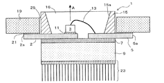
図1は,本発明の一実施形態の半導体発光素子1の構造を示す断面図である。本実施形態の半導体発光素子1は,第1及び第2リード2,5と,第1リード2上にダイボンディングされ,第2リード5にワイヤーボンディングされた半導体発光素子チップ3と,絶縁性接着層7を介して第1及び第2リード2,5に固着された放熱用金属体9とを有する。チップ3は,導電性接着層11を介して,第1リード2上にダイボンディングされている。チップ3は,ボンディングワイヤー13を介して第2リード5にワイヤーボンディングされている。
次に,素子1を配線基板に取り付けて構成した半導体発光素子アセンブリの2つの実施形態について説明する。
図2は,本発明の第1実施形態の半導体発光素子アセンブリの構造を示す断面図である。本実施形態のアセンブリは,半導体発光素子1と,放熱用金属体9を収容可能な開口部17を有する配線基板19とを備え,放熱用金属体9が開口部17に収容されるように,第1及び第2リード2,5が配線基板19に固着されている。第1及び第2リード2,5は,はんだ層21を介して固着されている。放熱用金属体9には,放熱器23が固着されている。放熱器23は,冷却フィンや水冷冷却器などからなる。
図3は,本発明の第2実施形態の半導体発光素子アセンブリの構造を示す断面図である。本実施形態のアセンブリは,半導体発光素子1と,反射器15を収容可能な開口部25を有する配線基板19とを備え,反射器15が開口部25に収容されるように,第1及び第2リード2,5が配線基板19に固着されている。第1及び第2リード2,5は,はんだ層21を介して固着されている。放熱用金属体9には,放熱器23が固着されている。放熱器23は,冷却フィンなどからなる。
次に,図1に示すような半導体発光素子の製造方法の一実施形態について,図4(a)〜(d)を用いて説明する。
まず,半導体発光素子チップ用の第1及び第2リード部2b,5bを有するリードフレーム27上に,反射面15aを有する反射器15を形成し,図4(a)に示す構造を得る。反射器15は,トランスファー成形によってテーパー上の開口部を有する樹脂層を形成し,この開口部の内面にアルミニウムや銀などの可視光に対して反射率の高い金属を蒸着して反射面15aを形成することによって,形成することができる。樹脂層の材料は,特に限定されないが,例えば,エポキシ樹脂にフィラ−(例えばシリカ)を混ぜたものを用いることができる。また,樹脂層の材料に酸化チタンを含んだ白色の樹脂を用いると,テーパー面をそのまま反射面とすることができるので,アルミニウムなどの蒸着工程を省略することができる。
また,トランスファー成型で反射層を作成する場合,リードと反射層をしっかりと固定するために,例えば,リードに貫通孔を設けて反射器を形成する樹脂をリードの裏側に回すと良い。該貫通孔はリードの下に放熱層が無い部分に設ければよい。
また,反射器を成型しておき,絶縁性接着シートでリードに圧着しても良い。
本工程は,任意であり,反射器15が不要な場合には,本工程を省略してもよい。
次に,リードフレーム27に,絶縁性接着層7を介して放熱用金属体9を固着し,図4(b)に示す構造を得る。
第1リード部2b上に半導体発光素子チップ3をダイボンディングし,チップ3と第2リード部5bをワイヤーボンディングする。ダイボンディング及びワイヤーボンディングは,それぞれ,導電性接着層11及びボンディングワイヤー13を介して行うことができる。
次に,リードフレーム27から枠部29を切り離すことによって,第1及び第2リード部2b,5bを切り出して,図4(d)に示す第1及び第2リード2,5を有する半導体発光素子1を得て,本実施形態を完了する。
上記実施例ではチップが1つの場合について説明したが複数のチップを有する場合も同様にして実施できることは容易に理解できるであろう。
Claims (12)
- 第1及び第2リードと,第1リード上にダイボンディングされ,第2リードにワイヤーボンディングされた半導体発光素子チップと,絶縁性接着層を介して第1及び第2リードに固着された放熱用金属体とを有する半導体発光素子。
- 前記絶縁性接着層は,絶縁性接着シートからなる請求項1に記載の素子。
- 絶縁性接着シートは,絶縁性支持層と,絶縁性支持層の両面に接着層とを備える請求項2に記載の素子。
- 第1及び第2リード上に固着され,前記チップからの光を反射させる反射器をさらに備える請求項1に記載の素子。
- 第1及び第2リードは,それぞれの先端まで,前記チップの光出射方向に垂直な方向に延びる請求項1に記載の素子。
- 請求項1に記載の素子と,
前記放熱用金属体を収容可能な開口部を有する配線基板とを備え,
前記放熱用金属体が前記開口部に収容されるように,第1及び第2リードが前記配線基板に固着されている半導体発光素子アセンブリ。 - 請求項4に記載の素子と,
前記反射器を収容可能な開口部を有する配線基板とを備え,
前記反射器が前記開口部に収容されるように,第1及び第2リードが前記配線基板に固着されている半導体発光素子アセンブリ。 - 第1及び第2リードは,その前記配線基板に対向する面全体で,前記配線基板に固着されている請求項6又は7に記載のアセンブリ。
- 前記放熱用金属体に固着された放熱器をさらに備える請求項6又は7に記載のアセンブリ。
- 半導体発光素子チップ用の第1及び第2リード部を有するリードフレームに,絶縁性接着層を介して放熱用金属体を固着し,
第1リード部上に半導体発光素子チップをダイボンディングし,
前記チップと第2リード部をワイヤーボンディングし,
前記リードフレームから第1及び第2リード部を切り出して,第1及び第2リードを有する半導体発光素子を得る工程を備える半導体発光素子の製造方法。 - 絶縁性接着層は,絶縁性接着シートからなり,放熱用金属体は,熱圧着により固着される請求項10に記載の方法。
- 絶縁性接着シートは,絶縁性支持層と,絶縁性支持層の両面に接着層とを備える請求項11に記載の方法。
Priority Applications (1)
| Application Number | Priority Date | Filing Date | Title |
|---|---|---|---|
| JP2006026025A JP2007208061A (ja) | 2006-02-02 | 2006-02-02 | 半導体発光素子,その製造方法,半導体発光素子アセンブリ |
Applications Claiming Priority (1)
| Application Number | Priority Date | Filing Date | Title |
|---|---|---|---|
| JP2006026025A JP2007208061A (ja) | 2006-02-02 | 2006-02-02 | 半導体発光素子,その製造方法,半導体発光素子アセンブリ |
Publications (1)
| Publication Number | Publication Date |
|---|---|
| JP2007208061A true JP2007208061A (ja) | 2007-08-16 |
Family
ID=38487246
Family Applications (1)
| Application Number | Title | Priority Date | Filing Date |
|---|---|---|---|
| JP2006026025A Pending JP2007208061A (ja) | 2006-02-02 | 2006-02-02 | 半導体発光素子,その製造方法,半導体発光素子アセンブリ |
Country Status (1)
| Country | Link |
|---|---|
| JP (1) | JP2007208061A (ja) |
Cited By (3)
| Publication number | Priority date | Publication date | Assignee | Title |
|---|---|---|---|---|
| JP2011054473A (ja) * | 2009-09-03 | 2011-03-17 | Koito Mfg Co Ltd | 車両用灯具 |
| WO2011083703A1 (ja) * | 2010-01-07 | 2011-07-14 | 国立大学法人九州工業大学 | Ledモジュール装置及びその製造方法 |
| US8546827B2 (en) | 2009-12-03 | 2013-10-01 | Stanley Electric Co., Ltd. | Semiconductor light emitting device |
Citations (7)
| Publication number | Priority date | Publication date | Assignee | Title |
|---|---|---|---|---|
| JP2000353828A (ja) * | 1999-06-11 | 2000-12-19 | Stanley Electric Co Ltd | 光電変換素子およびその製造方法 |
| JP2004214436A (ja) * | 2003-01-06 | 2004-07-29 | Sharp Corp | 半導体発光装置およびその製造方法 |
| WO2005048358A1 (de) * | 2003-11-07 | 2005-05-26 | Tridonic Optoelectronics Gmbh | Leuchtdioden-anordnung mit wärmeabführender platine |
| JP2005136224A (ja) * | 2003-10-30 | 2005-05-26 | Asahi Kasei Electronics Co Ltd | 発光ダイオード照明モジュール |
| JP2005217369A (ja) * | 2004-02-02 | 2005-08-11 | Three M Innovative Properties Co | 発光ダイオード装置用接着シート及び発光ダイオード装置 |
| WO2005091387A1 (ja) * | 2004-03-24 | 2005-09-29 | Toshiba Lighting & Technology Corporation | 発光装置および照明装置 |
| JP2006005290A (ja) * | 2004-06-21 | 2006-01-05 | Citizen Electronics Co Ltd | 発光ダイオード |
-
2006
- 2006-02-02 JP JP2006026025A patent/JP2007208061A/ja active Pending
Patent Citations (7)
| Publication number | Priority date | Publication date | Assignee | Title |
|---|---|---|---|---|
| JP2000353828A (ja) * | 1999-06-11 | 2000-12-19 | Stanley Electric Co Ltd | 光電変換素子およびその製造方法 |
| JP2004214436A (ja) * | 2003-01-06 | 2004-07-29 | Sharp Corp | 半導体発光装置およびその製造方法 |
| JP2005136224A (ja) * | 2003-10-30 | 2005-05-26 | Asahi Kasei Electronics Co Ltd | 発光ダイオード照明モジュール |
| WO2005048358A1 (de) * | 2003-11-07 | 2005-05-26 | Tridonic Optoelectronics Gmbh | Leuchtdioden-anordnung mit wärmeabführender platine |
| JP2005217369A (ja) * | 2004-02-02 | 2005-08-11 | Three M Innovative Properties Co | 発光ダイオード装置用接着シート及び発光ダイオード装置 |
| WO2005091387A1 (ja) * | 2004-03-24 | 2005-09-29 | Toshiba Lighting & Technology Corporation | 発光装置および照明装置 |
| JP2006005290A (ja) * | 2004-06-21 | 2006-01-05 | Citizen Electronics Co Ltd | 発光ダイオード |
Cited By (3)
| Publication number | Priority date | Publication date | Assignee | Title |
|---|---|---|---|---|
| JP2011054473A (ja) * | 2009-09-03 | 2011-03-17 | Koito Mfg Co Ltd | 車両用灯具 |
| US8546827B2 (en) | 2009-12-03 | 2013-10-01 | Stanley Electric Co., Ltd. | Semiconductor light emitting device |
| WO2011083703A1 (ja) * | 2010-01-07 | 2011-07-14 | 国立大学法人九州工業大学 | Ledモジュール装置及びその製造方法 |
Similar Documents
| Publication | Publication Date | Title |
|---|---|---|
| JP4757495B2 (ja) | 複合リードフレームledパッケージおよびその製造方法 | |
| US7462880B2 (en) | Semiconductor light-emitting element assembly | |
| US8421088B2 (en) | Surface mounting type light emitting diode | |
| JP4808550B2 (ja) | 発光ダイオード光源装置、照明装置、表示装置及び交通信号機 | |
| JP5106094B2 (ja) | 表面実装型発光ダイオードおよびその製造方法 | |
| JP2006339224A (ja) | Led用基板およびledパッケージ | |
| JP2007300110A (ja) | 発光装置 | |
| JP2003168829A (ja) | 発光装置 | |
| JP2006313896A (ja) | 発光素子パッケージ | |
| JP2003152225A (ja) | 発光装置 | |
| JP2005117041A (ja) | 高出力発光ダイオードデバイス | |
| JP2007513520A (ja) | 発光ダイオードに基づく照明組立体 | |
| JP2007234846A (ja) | 発光素子用セラミックパッケージ | |
| JP2009054801A (ja) | 放熱部材及びそれを備えた発光モジュール | |
| JP2010109119A (ja) | 発光モジュール及びその製造方法 | |
| JP2008085302A (ja) | 照明装置 | |
| JP4114557B2 (ja) | 発光装置 | |
| JP2008218763A (ja) | 発光装置 | |
| JP5057371B2 (ja) | 表面実装型発光ダイオードおよびその製造方法 | |
| JP2009231397A (ja) | 照明装置 | |
| JP4679917B2 (ja) | 半導体発光装置 | |
| JP2007300111A (ja) | 発光装置 | |
| JP2007208061A (ja) | 半導体発光素子,その製造方法,半導体発光素子アセンブリ | |
| JP4831958B2 (ja) | 表面実装型led | |
| JP2008124297A (ja) | 発光装置 |
Legal Events
| Date | Code | Title | Description |
|---|---|---|---|
| A621 | Written request for application examination |
Free format text: JAPANESE INTERMEDIATE CODE: A621 Effective date: 20080220 |
|
| A131 | Notification of reasons for refusal |
Free format text: JAPANESE INTERMEDIATE CODE: A131 Effective date: 20100831 |
|
| A977 | Report on retrieval |
Free format text: JAPANESE INTERMEDIATE CODE: A971007 Effective date: 20100831 |
|
| A521 | Written amendment |
Free format text: JAPANESE INTERMEDIATE CODE: A523 Effective date: 20101027 |
|
| A131 | Notification of reasons for refusal |
Free format text: JAPANESE INTERMEDIATE CODE: A131 Effective date: 20110719 |
|
| A521 | Written amendment |
Free format text: JAPANESE INTERMEDIATE CODE: A523 Effective date: 20110909 |
|
| A02 | Decision of refusal |
Free format text: JAPANESE INTERMEDIATE CODE: A02 Effective date: 20120403 |