JP2007201093A - Nitride semiconductor device - Google Patents
Nitride semiconductor device Download PDFInfo
- Publication number
- JP2007201093A JP2007201093A JP2006016622A JP2006016622A JP2007201093A JP 2007201093 A JP2007201093 A JP 2007201093A JP 2006016622 A JP2006016622 A JP 2006016622A JP 2006016622 A JP2006016622 A JP 2006016622A JP 2007201093 A JP2007201093 A JP 2007201093A
- Authority
- JP
- Japan
- Prior art keywords
- layer
- nitride semiconductor
- semiconductor layer
- semiconductor device
- nitride
- Prior art date
- Legal status (The legal status is an assumption and is not a legal conclusion. Google has not performed a legal analysis and makes no representation as to the accuracy of the status listed.)
- Granted
Links
- 239000004065 semiconductor Substances 0.000 title claims abstract description 197
- 150000004767 nitrides Chemical class 0.000 title claims abstract description 96
- 229910052782 aluminium Inorganic materials 0.000 claims abstract description 9
- 239000000203 mixture Substances 0.000 claims description 24
- 238000005036 potential barrier Methods 0.000 claims description 14
- XAGFODPZIPBFFR-UHFFFAOYSA-N aluminium Chemical compound [Al] XAGFODPZIPBFFR-UHFFFAOYSA-N 0.000 claims description 5
- 229910052738 indium Inorganic materials 0.000 claims description 4
- APFVFJFRJDLVQX-UHFFFAOYSA-N indium atom Chemical compound [In] APFVFJFRJDLVQX-UHFFFAOYSA-N 0.000 claims description 4
- 238000005259 measurement Methods 0.000 claims description 2
- 239000000758 substrate Substances 0.000 abstract description 19
- 229910052594 sapphire Inorganic materials 0.000 abstract description 8
- 239000010980 sapphire Substances 0.000 abstract description 8
- 229910052719 titanium Inorganic materials 0.000 abstract description 5
- JMASRVWKEDWRBT-UHFFFAOYSA-N Gallium nitride Chemical compound [Ga]#N JMASRVWKEDWRBT-UHFFFAOYSA-N 0.000 description 32
- 229910002601 GaN Inorganic materials 0.000 description 31
- 239000000463 material Substances 0.000 description 17
- 229910002704 AlGaN Inorganic materials 0.000 description 11
- 238000002161 passivation Methods 0.000 description 10
- 230000010287 polarization Effects 0.000 description 10
- 230000005669 field effect Effects 0.000 description 7
- PXHVJJICTQNCMI-UHFFFAOYSA-N Nickel Chemical compound [Ni] PXHVJJICTQNCMI-UHFFFAOYSA-N 0.000 description 6
- PMHQVHHXPFUNSP-UHFFFAOYSA-M copper(1+);methylsulfanylmethane;bromide Chemical compound Br[Cu].CSC PMHQVHHXPFUNSP-UHFFFAOYSA-M 0.000 description 6
- 238000010586 diagram Methods 0.000 description 6
- 229910052581 Si3N4 Inorganic materials 0.000 description 5
- 230000007423 decrease Effects 0.000 description 5
- HQVNEWCFYHHQES-UHFFFAOYSA-N silicon nitride Chemical compound N12[Si]34N5[Si]62N3[Si]51N64 HQVNEWCFYHHQES-UHFFFAOYSA-N 0.000 description 5
- 239000010936 titanium Substances 0.000 description 5
- 230000005533 two-dimensional electron gas Effects 0.000 description 5
- KDLHZDBZIXYQEI-UHFFFAOYSA-N Palladium Chemical compound [Pd] KDLHZDBZIXYQEI-UHFFFAOYSA-N 0.000 description 4
- 230000000052 comparative effect Effects 0.000 description 4
- 238000005530 etching Methods 0.000 description 3
- 239000012535 impurity Substances 0.000 description 3
- 239000011777 magnesium Substances 0.000 description 3
- 230000002269 spontaneous effect Effects 0.000 description 3
- 230000004888 barrier function Effects 0.000 description 2
- 150000001875 compounds Chemical class 0.000 description 2
- 239000003574 free electron Substances 0.000 description 2
- 125000005842 heteroatom Chemical group 0.000 description 2
- 238000002347 injection Methods 0.000 description 2
- 239000007924 injection Substances 0.000 description 2
- 238000005215 recombination Methods 0.000 description 2
- 230000006798 recombination Effects 0.000 description 2
- PIGFYZPCRLYGLF-UHFFFAOYSA-N Aluminum nitride Chemical compound [Al]#N PIGFYZPCRLYGLF-UHFFFAOYSA-N 0.000 description 1
- JBRZTFJDHDCESZ-UHFFFAOYSA-N AsGa Chemical compound [As]#[Ga] JBRZTFJDHDCESZ-UHFFFAOYSA-N 0.000 description 1
- ZOXJGFHDIHLPTG-UHFFFAOYSA-N Boron Chemical compound [B] ZOXJGFHDIHLPTG-UHFFFAOYSA-N 0.000 description 1
- FYYHWMGAXLPEAU-UHFFFAOYSA-N Magnesium Chemical compound [Mg] FYYHWMGAXLPEAU-UHFFFAOYSA-N 0.000 description 1
- XUIMIQQOPSSXEZ-UHFFFAOYSA-N Silicon Chemical compound [Si] XUIMIQQOPSSXEZ-UHFFFAOYSA-N 0.000 description 1
- RTAQQCXQSZGOHL-UHFFFAOYSA-N Titanium Chemical compound [Ti] RTAQQCXQSZGOHL-UHFFFAOYSA-N 0.000 description 1
- 238000009825 accumulation Methods 0.000 description 1
- 229910052785 arsenic Inorganic materials 0.000 description 1
- RQNWIZPPADIBDY-UHFFFAOYSA-N arsenic atom Chemical compound [As] RQNWIZPPADIBDY-UHFFFAOYSA-N 0.000 description 1
- NWAIGJYBQQYSPW-UHFFFAOYSA-N azanylidyneindigane Chemical compound [In]#N NWAIGJYBQQYSPW-UHFFFAOYSA-N 0.000 description 1
- 229910052796 boron Inorganic materials 0.000 description 1
- 239000000969 carrier Substances 0.000 description 1
- 230000015556 catabolic process Effects 0.000 description 1
- 239000013078 crystal Substances 0.000 description 1
- 230000003247 decreasing effect Effects 0.000 description 1
- 230000005684 electric field Effects 0.000 description 1
- 238000005468 ion implantation Methods 0.000 description 1
- 150000002500 ions Chemical class 0.000 description 1
- 238000002955 isolation Methods 0.000 description 1
- 229910052749 magnesium Inorganic materials 0.000 description 1
- 229910052751 metal Inorganic materials 0.000 description 1
- 239000002184 metal Substances 0.000 description 1
- 238000000034 method Methods 0.000 description 1
- 229910052759 nickel Inorganic materials 0.000 description 1
- TWNQGVIAIRXVLR-UHFFFAOYSA-N oxo(oxoalumanyloxy)alumane Chemical compound O=[Al]O[Al]=O TWNQGVIAIRXVLR-UHFFFAOYSA-N 0.000 description 1
- 229910052763 palladium Inorganic materials 0.000 description 1
- 230000000717 retained effect Effects 0.000 description 1
- 229910052710 silicon Inorganic materials 0.000 description 1
- 239000010703 silicon Substances 0.000 description 1
- HBMJWWWQQXIZIP-UHFFFAOYSA-N silicon carbide Chemical compound [Si+]#[C-] HBMJWWWQQXIZIP-UHFFFAOYSA-N 0.000 description 1
- 238000004088 simulation Methods 0.000 description 1
Images


Classifications
-
- H—ELECTRICITY
- H01—ELECTRIC ELEMENTS
- H01L—SEMICONDUCTOR DEVICES NOT COVERED BY CLASS H10
- H01L29/00—Semiconductor devices adapted for rectifying, amplifying, oscillating or switching, or capacitors or resistors with at least one potential-jump barrier or surface barrier, e.g. PN junction depletion layer or carrier concentration layer; Details of semiconductor bodies or of electrodes thereof ; Multistep manufacturing processes therefor
- H01L29/66—Types of semiconductor device ; Multistep manufacturing processes therefor
- H01L29/68—Types of semiconductor device ; Multistep manufacturing processes therefor controllable by only the electric current supplied, or only the electric potential applied, to an electrode which does not carry the current to be rectified, amplified or switched
- H01L29/76—Unipolar devices, e.g. field effect transistors
- H01L29/772—Field effect transistors
- H01L29/778—Field effect transistors with two-dimensional charge carrier gas channel, e.g. HEMT ; with two-dimensional charge-carrier layer formed at a heterojunction interface
- H01L29/7782—Field effect transistors with two-dimensional charge carrier gas channel, e.g. HEMT ; with two-dimensional charge-carrier layer formed at a heterojunction interface with confinement of carriers by at least two heterojunctions, e.g. DHHEMT, quantum well HEMT, DHMODFET
- H01L29/7783—Field effect transistors with two-dimensional charge carrier gas channel, e.g. HEMT ; with two-dimensional charge-carrier layer formed at a heterojunction interface with confinement of carriers by at least two heterojunctions, e.g. DHHEMT, quantum well HEMT, DHMODFET using III-V semiconductor material
-
- H—ELECTRICITY
- H01—ELECTRIC ELEMENTS
- H01L—SEMICONDUCTOR DEVICES NOT COVERED BY CLASS H10
- H01L29/00—Semiconductor devices adapted for rectifying, amplifying, oscillating or switching, or capacitors or resistors with at least one potential-jump barrier or surface barrier, e.g. PN junction depletion layer or carrier concentration layer; Details of semiconductor bodies or of electrodes thereof ; Multistep manufacturing processes therefor
- H01L29/02—Semiconductor bodies ; Multistep manufacturing processes therefor
- H01L29/06—Semiconductor bodies ; Multistep manufacturing processes therefor characterised by their shape; characterised by the shapes, relative sizes, or dispositions of the semiconductor regions ; characterised by the concentration or distribution of impurities within semiconductor regions
- H01L29/10—Semiconductor bodies ; Multistep manufacturing processes therefor characterised by their shape; characterised by the shapes, relative sizes, or dispositions of the semiconductor regions ; characterised by the concentration or distribution of impurities within semiconductor regions with semiconductor regions connected to an electrode not carrying current to be rectified, amplified or switched and such electrode being part of a semiconductor device which comprises three or more electrodes
- H01L29/1066—Gate region of field-effect devices with PN junction gate
-
- H—ELECTRICITY
- H01—ELECTRIC ELEMENTS
- H01L—SEMICONDUCTOR DEVICES NOT COVERED BY CLASS H10
- H01L29/00—Semiconductor devices adapted for rectifying, amplifying, oscillating or switching, or capacitors or resistors with at least one potential-jump barrier or surface barrier, e.g. PN junction depletion layer or carrier concentration layer; Details of semiconductor bodies or of electrodes thereof ; Multistep manufacturing processes therefor
- H01L29/40—Electrodes ; Multistep manufacturing processes therefor
- H01L29/43—Electrodes ; Multistep manufacturing processes therefor characterised by the materials of which they are formed
- H01L29/432—Heterojunction gate for field effect devices
-
- H—ELECTRICITY
- H01—ELECTRIC ELEMENTS
- H01L—SEMICONDUCTOR DEVICES NOT COVERED BY CLASS H10
- H01L29/00—Semiconductor devices adapted for rectifying, amplifying, oscillating or switching, or capacitors or resistors with at least one potential-jump barrier or surface barrier, e.g. PN junction depletion layer or carrier concentration layer; Details of semiconductor bodies or of electrodes thereof ; Multistep manufacturing processes therefor
- H01L29/66—Types of semiconductor device ; Multistep manufacturing processes therefor
- H01L29/68—Types of semiconductor device ; Multistep manufacturing processes therefor controllable by only the electric current supplied, or only the electric potential applied, to an electrode which does not carry the current to be rectified, amplified or switched
- H01L29/76—Unipolar devices, e.g. field effect transistors
- H01L29/772—Field effect transistors
- H01L29/778—Field effect transistors with two-dimensional charge carrier gas channel, e.g. HEMT ; with two-dimensional charge-carrier layer formed at a heterojunction interface
- H01L29/7786—Field effect transistors with two-dimensional charge carrier gas channel, e.g. HEMT ; with two-dimensional charge-carrier layer formed at a heterojunction interface with direct single heterostructure, i.e. with wide bandgap layer formed on top of active layer, e.g. direct single heterostructure MIS-like HEMT
- H01L29/7787—Field effect transistors with two-dimensional charge carrier gas channel, e.g. HEMT ; with two-dimensional charge-carrier layer formed at a heterojunction interface with direct single heterostructure, i.e. with wide bandgap layer formed on top of active layer, e.g. direct single heterostructure MIS-like HEMT with wide bandgap charge-carrier supplying layer, e.g. direct single heterostructure MODFET
-
- H—ELECTRICITY
- H01—ELECTRIC ELEMENTS
- H01L—SEMICONDUCTOR DEVICES NOT COVERED BY CLASS H10
- H01L21/00—Processes or apparatus adapted for the manufacture or treatment of semiconductor or solid state devices or of parts thereof
- H01L21/02—Manufacture or treatment of semiconductor devices or of parts thereof
- H01L21/02104—Forming layers
- H01L21/02365—Forming inorganic semiconducting materials on a substrate
- H01L21/02367—Substrates
- H01L21/0237—Materials
- H01L21/02373—Group 14 semiconducting materials
- H01L21/02381—Silicon, silicon germanium, germanium
-
- H—ELECTRICITY
- H01—ELECTRIC ELEMENTS
- H01L—SEMICONDUCTOR DEVICES NOT COVERED BY CLASS H10
- H01L21/00—Processes or apparatus adapted for the manufacture or treatment of semiconductor or solid state devices or of parts thereof
- H01L21/02—Manufacture or treatment of semiconductor devices or of parts thereof
- H01L21/02104—Forming layers
- H01L21/02365—Forming inorganic semiconducting materials on a substrate
- H01L21/02367—Substrates
- H01L21/0237—Materials
- H01L21/0242—Crystalline insulating materials
-
- H—ELECTRICITY
- H01—ELECTRIC ELEMENTS
- H01L—SEMICONDUCTOR DEVICES NOT COVERED BY CLASS H10
- H01L21/00—Processes or apparatus adapted for the manufacture or treatment of semiconductor or solid state devices or of parts thereof
- H01L21/02—Manufacture or treatment of semiconductor devices or of parts thereof
- H01L21/02104—Forming layers
- H01L21/02365—Forming inorganic semiconducting materials on a substrate
- H01L21/02436—Intermediate layers between substrates and deposited layers
- H01L21/02439—Materials
- H01L21/02455—Group 13/15 materials
- H01L21/02458—Nitrides
-
- H—ELECTRICITY
- H01—ELECTRIC ELEMENTS
- H01L—SEMICONDUCTOR DEVICES NOT COVERED BY CLASS H10
- H01L21/00—Processes or apparatus adapted for the manufacture or treatment of semiconductor or solid state devices or of parts thereof
- H01L21/02—Manufacture or treatment of semiconductor devices or of parts thereof
- H01L21/02104—Forming layers
- H01L21/02365—Forming inorganic semiconducting materials on a substrate
- H01L21/02436—Intermediate layers between substrates and deposited layers
- H01L21/02494—Structure
- H01L21/02496—Layer structure
- H01L21/02502—Layer structure consisting of two layers
-
- H—ELECTRICITY
- H01—ELECTRIC ELEMENTS
- H01L—SEMICONDUCTOR DEVICES NOT COVERED BY CLASS H10
- H01L21/00—Processes or apparatus adapted for the manufacture or treatment of semiconductor or solid state devices or of parts thereof
- H01L21/02—Manufacture or treatment of semiconductor devices or of parts thereof
- H01L21/02104—Forming layers
- H01L21/02365—Forming inorganic semiconducting materials on a substrate
- H01L21/02518—Deposited layers
- H01L21/02521—Materials
- H01L21/02538—Group 13/15 materials
- H01L21/0254—Nitrides
-
- H—ELECTRICITY
- H01—ELECTRIC ELEMENTS
- H01L—SEMICONDUCTOR DEVICES NOT COVERED BY CLASS H10
- H01L29/00—Semiconductor devices adapted for rectifying, amplifying, oscillating or switching, or capacitors or resistors with at least one potential-jump barrier or surface barrier, e.g. PN junction depletion layer or carrier concentration layer; Details of semiconductor bodies or of electrodes thereof ; Multistep manufacturing processes therefor
- H01L29/02—Semiconductor bodies ; Multistep manufacturing processes therefor
- H01L29/12—Semiconductor bodies ; Multistep manufacturing processes therefor characterised by the materials of which they are formed
- H01L29/20—Semiconductor bodies ; Multistep manufacturing processes therefor characterised by the materials of which they are formed including, apart from doping materials or other impurities, only AIIIBV compounds
- H01L29/2003—Nitride compounds
-
- H—ELECTRICITY
- H01—ELECTRIC ELEMENTS
- H01L—SEMICONDUCTOR DEVICES NOT COVERED BY CLASS H10
- H01L29/00—Semiconductor devices adapted for rectifying, amplifying, oscillating or switching, or capacitors or resistors with at least one potential-jump barrier or surface barrier, e.g. PN junction depletion layer or carrier concentration layer; Details of semiconductor bodies or of electrodes thereof ; Multistep manufacturing processes therefor
- H01L29/40—Electrodes ; Multistep manufacturing processes therefor
- H01L29/41—Electrodes ; Multistep manufacturing processes therefor characterised by their shape, relative sizes or dispositions
- H01L29/417—Electrodes ; Multistep manufacturing processes therefor characterised by their shape, relative sizes or dispositions carrying the current to be rectified, amplified or switched
- H01L29/41725—Source or drain electrodes for field effect devices
- H01L29/4175—Source or drain electrodes for field effect devices for lateral devices where the connection to the source or drain region is done through at least one part of the semiconductor substrate thickness, e.g. with connecting sink or with via-hole
-
- H—ELECTRICITY
- H01—ELECTRIC ELEMENTS
- H01L—SEMICONDUCTOR DEVICES NOT COVERED BY CLASS H10
- H01L29/00—Semiconductor devices adapted for rectifying, amplifying, oscillating or switching, or capacitors or resistors with at least one potential-jump barrier or surface barrier, e.g. PN junction depletion layer or carrier concentration layer; Details of semiconductor bodies or of electrodes thereof ; Multistep manufacturing processes therefor
- H01L29/40—Electrodes ; Multistep manufacturing processes therefor
- H01L29/43—Electrodes ; Multistep manufacturing processes therefor characterised by the materials of which they are formed
- H01L29/45—Ohmic electrodes
- H01L29/452—Ohmic electrodes on AIII-BV compounds
Abstract
Description
本発明は、窒化ガリウム(GaN)を主成分とするIII−V族窒化物半導体からなり、正電圧動作(ノーマリオフ動作)が可能な窒化物半導体装置に関する。 The present invention relates to a nitride semiconductor device made of a group III-V nitride semiconductor containing gallium nitride (GaN) as a main component and capable of a positive voltage operation (normally off operation).
近年、高周波大電力デバイスとしてGaN系の化合物半導体材料を用いた電界効果トランジスタ(Field Effect Transistor、以下FETと表記する。)の研究が活発に行われている。GaN等の窒化物半導体材料は窒化アルミニウム(AlN)又は窒化インジウム(InN)と種々の混晶を作ることができるため、従来から用いられている砒化ガリウム(GaAs)を主成分とする砒素系半導体材料と同様にヘテロ接合を形成することができる。しかし、窒化物半導体におけるヘテロ接合では、ドーピングされていない状態でも接合面に窒化物半導体が有する自発分極又はピエゾ分極によって生じる高濃度のキャリアが発生する。このため、FETを作製した場合にはデプレッション型(ノーマリオン型)になり易く、エンハンスメント型(ノーマリオフ型)の特性を得ることが難しい。現在、パワーエレクトロニクス市場に一般に流通しているデバイスはノーマリオフ型であり、GaN系の窒化物半導体装置に対してもノーマリオフ型が強く求められている。 In recent years, field effect transistors (hereinafter referred to as FETs) using GaN-based compound semiconductor materials as high-frequency, high-power devices have been actively researched. Since nitride semiconductor materials such as GaN can form various mixed crystals with aluminum nitride (AlN) or indium nitride (InN), arsenic semiconductors mainly composed of gallium arsenide (GaAs) that have been used in the past. A heterojunction can be formed in the same manner as the material. However, in a heterojunction in a nitride semiconductor, a high concentration of carriers generated by spontaneous polarization or piezoelectric polarization of the nitride semiconductor is generated on the junction surface even in an undoped state. For this reason, when an FET is manufactured, it tends to be a depletion type (normally on type), and it is difficult to obtain an enhancement type (normally off type) characteristic. Currently, devices that are generally distributed in the power electronics market are normally-off devices, and there is a strong demand for normally-off devices for GaN-based nitride semiconductor devices.
以下、従来の窒化物半導体材料を用いたFETについて説明する。 A conventional FET using a nitride semiconductor material will be described below.
図7に示すように、従来のAlGaNとGaNとのへテロ接合を用いたFETは、主面の面方位が(0001)面であるサファイアからなる基板701と、基板701の主面上に形成されたアンドープGaN層702と、アンドープGaN層702の上に形成されたアンドープAl0.25Ga0.75N層703とを有している。
As shown in FIG. 7, a conventional FET using AlGaN and GaN heterojunction is formed on a main surface of a
また、アンドープAl0.25Ga0.75N層703の上にチタン(Ti)及びアルミニウム(Al)からなるソース電極704並びにドレイン電極705が形成され、ソース電極704とドレイン電極705との間にパラジウム(Pd)からなるゲート電極706が形成されている。さらに、アンドープAl0.25Ga0.75N層703の上面で且つソース電極704、ドレイン電極705及びゲート電極706が形成されていない領域に窒化シリコン(SiN)からなるパッシベーション膜707が形成されている。
A
アンドープGaN層702とアンドープAl0.25Ga0.75N層703とのヘテロ接合面には、アンドープAl0.25Ga0.75N層703が有する自発分極及びピエゾ分極のために、1×1013cm-2程度の2次元電子ガス層が形成されている。
The heterojunction surface between the
このことは、図8に示すように、従来のFETにおいて分極によって生じる固定電荷と自由電子の分布から説明される。すなわち、アンドープGaN層702及びアンドープAl0.25Ga0.75N層703の上面にそれぞれ負の固定電荷が形成され、また、それぞれの下面に正の固定電荷が形成される。このことを図8において、アンドープAl0.25Ga0.75N層703に形成される固定電荷を実線、アンドープGaN層702に形成される固定電荷を破線で示す。このように、アンドープAl0.25Ga0.75N層703に形成される固定電荷の量がアンドープGaN層702に形成される固定電荷の量よりも大きいため、ヘテロ接合面に固定電荷の量の差を補償する量のシートキャリアが2次元電子ガス層の形で形成される(図8の太線、Nsで示す。)。
This is explained from the distribution of fixed charges and free electrons generated by polarization in a conventional FET, as shown in FIG. That is, negative fixed charges are formed on the upper surfaces of the
この分極によってアンドープGaN層702及びアンドープAl0.25Ga0.75N層703に電界が生じるため、従来のFETのエネルギーバンドが図9に示すようになる。従って、図10に示すように、ゲート電圧とドレイン電流との電気特性は、基本的にノーマリオンの特性を示すことになる。
This polarization generates an electric field in the
また、ソース電極704及びドレイン電極705はアンドープAl0.25Ga0.75N層703に接するように形成されるが、アンドープAl0.25Ga0.75N層703の膜厚が例えば30nm以下と薄い場合には、ソース電極704及びドレイン電極705は、トンネル電流によりヘテロ接合面に形成される高濃度の2次元電子ガス層と接続可能となるため、良好なオーミック接触となる。また、ゲート電極706は5.1eVの大きな仕事関数を有しており、アンドープAl0.25Ga0.75N層703に対して良好なショットキ接合となる(非特許文献1を参照。)。
Also, if the
このように、ノーマリオン型になり易いGaN系の化合物半導体材料を用いてノーマリオフ型の動作特性を実現するには、GaN系の窒化物半導体材料が有する自発分極及びピエゾ分極によってチャネル内に生成されるキャリアを減らす必要がある。従来のAlGaN層とGaN層とのヘテロ接合を用いたFETの場合は、AlGaN層中のAl組成を下げればGaN層との格子定数差によるストレスが低減できるため、ピエゾ分極を減少させることができ、その結果、シートキャリア濃度を減少させることが可能である(非特許文献2を参照。)。 Thus, in order to realize normally-off type operating characteristics using a GaN-based compound semiconductor material that tends to be normally-on, it is generated in the channel by the spontaneous polarization and piezo-polarization of the GaN-based nitride semiconductor material. There is a need to reduce careers. In the case of a conventional FET using a heterojunction between an AlGaN layer and a GaN layer, if the Al composition in the AlGaN layer is lowered, the stress due to the difference in lattice constant from the GaN layer can be reduced, so that piezoelectric polarization can be reduced. As a result, it is possible to reduce the sheet carrier concentration (see Non-Patent Document 2).
具体的に図7に示すアンドープAl0.25Ga0.75N層703を膜厚30nmのままでAlの組成を0.25から0.15に低下させると、シートキャリア濃度は1.2×1013cm-2から5×1012cm-2まで大幅に減少させることができる。しかし、シートキャリア濃度の減少に伴い、動作電流が低減するだけでなく、アンドープAl0.25Ga0.75N層703のAl組成の低下に伴い、ゲート部のポテンシャルバリアも低下する。また、ゲート電極でのリーク電流の発生を抑えるために、ゲート電極706に印加可能な順方向電圧には上限がある。
Specifically, when the undoped Al 0.25 Ga 0.75
従って、ノーマリオフ型で且つより大きな順方向電圧を印加可能とするためには、ゲート部をp型領域化させることで、ポテンシャルバリアを高めることが一つの方法である。このような特徴を有するFETが、接合型FET(Junction Field Effect Transistor、以下JFETと表記する。)である(非特許文献3及び特許文献1を参照。)。
Therefore, in order to be able to apply a normally-off type and a larger forward voltage, it is one method to increase the potential barrier by making the gate portion a p-type region. An FET having such characteristics is a junction FET (Junction Field Effect Transistor, hereinafter referred to as JFET) (see Non-Patent
しかしながら、JFETをノーマリオフ化した場合、ゲート電極に順方向バイアスを印加しても予めチャネルに生成される電子濃度を大きくすることが困難であった。また、ゲート電極に対して順方向バイアスを印加できるのはゲートから電流が流れ始めるまでであり、具体的にはバンドギャップを考慮して3V程度までが限界であった。このことにより、これまでのJFETではドレイン動作電流を大きくすることが困難であるという問題があった。 However, when the JFET is normally off, it is difficult to increase the concentration of electrons generated in the channel in advance even if a forward bias is applied to the gate electrode. In addition, the forward bias can be applied to the gate electrode until the current starts to flow from the gate. Specifically, the limit is about 3 V in consideration of the band gap. As a result, the conventional JFET has a problem that it is difficult to increase the drain operating current.
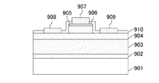
図11はこの問題を解決するための比較例である窒化物半導体装置の断面図を示している。 FIG. 11 is a sectional view of a nitride semiconductor device which is a comparative example for solving this problem.
図11に示すように、従来の課題を解決する比較例である窒化物半導体装置は、主面の面方位が(0001)面であるサファイアからなる基板901と、基板901の主面上に形成されたAlNバッファ層902と、AlNバッファ層902の上に形成されたアンドープGaN層903と、アンドープGaN層903の上に形成されたアンドープAlGaN層904と、アンドープAlGaN層904の一部の上に形成され、p型不純物を含むAlGaNで構成されたp型コントロール層905と、p型コントロール層905の上に形成されp型コントロール層905よりも高濃度のp型不純物を含むGaNで構成されたp型コンタクト層906とを有している。
As shown in FIG. 11, a nitride semiconductor device, which is a comparative example for solving the conventional problems, is formed on a main surface of a
また、p型コンタクト層906の上で、p型コンタクト層906とオーミック接触するゲート電極907と、p型コンタクト層906を挟むようにしてアンドープAlGaN層904の上に形成されたソース電極908及びドレイン電極909と、ゲート電極907、ソース電極908及びドレイン電極909以外の上部表面に形成されたパッシベーション膜910とが形成されている。
Further, a
上記の窒化物半導体装置において、アンドープAlGaN層904のバンドギャップは、チャネル領域であるアンドープGaN層903のバンドギャップよりも大きい。アンドープAlGaN層904とp型コントロール層905とは同一の材料からなるため、p型コントロール領域を形成するp型コントロール層905のバンドギャップもアンドープGaN層903のバンドギャップよりも大きい。また、アンドープGaN層903とアンドープAlGaN層904との界面にはヘテロ障壁が形成されており、半導体装置の動作時に2次元電子ガス層が形成されている。
In the nitride semiconductor device described above, the band gap of the undoped AlGaN
このように、窒化物半導体からなるチャネル領域(アンドープGaN層903)の上にバンドギャップが大きいp型コントロール領域(p型コントロール層905)を設け、該p型コントロール領域をチャネル領域に対して順方向にバイアスをかけることにより、チャネル領域内にホールが注入される。このようにすると、チャネル領域内にホールと同量の電子が発生するため、大きな動作電流を得ることができる。このような構造により、チャネル領域に注入されたホールによってチャネル領域内の電子の発生を促し、チャネル領域を流れる電流量を飛躍的に増加させることが可能である。 Thus, a p-type control region (p-type control layer 905) having a large band gap is provided on a channel region (undoped GaN layer 903) made of a nitride semiconductor, and the p-type control region is arranged in order with respect to the channel region. By biasing in the direction, holes are injected into the channel region. In this way, the same amount of electrons as holes are generated in the channel region, so that a large operating current can be obtained. With such a structure, generation of electrons in the channel region can be promoted by holes injected into the channel region, and the amount of current flowing through the channel region can be dramatically increased.
また、窒化物半導体におけるホールの移動度は電子の移動度に比べて非常に小さいため、窒化物半導体で構成されるチャネル領域へ注入されたホールは電流を流す単体として殆ど寄与しなくなる。従って、p型コントロール領域から注入されたホールは同量の電子をチャネル領域に生成し、動作電流を増大させることが可能となる。チャネル領域に注入されたホールの移動度が0に近いほど、ホールはドナーイオンのような役割を果たすことになるため、チャネル領域でキャリア濃度の変調を行うことが可能となる。このため、大きな動作電流を有するノーマリオフ型の窒化物半導体装置を実現できることになる。 In addition, since the mobility of holes in the nitride semiconductor is much smaller than the mobility of electrons, the holes injected into the channel region formed of the nitride semiconductor hardly contribute as a single unit for passing current. Therefore, holes injected from the p-type control region generate the same amount of electrons in the channel region, and the operating current can be increased. As the mobility of holes injected into the channel region is closer to 0, the hole plays a role like a donor ion, and thus the carrier concentration can be modulated in the channel region. Therefore, a normally-off type nitride semiconductor device having a large operating current can be realized.
このような構造はJFETに類似しているが、ゲート電極の接合面でチャネル領域内のキャリア濃度の変調を行う接合型電界効果トランジスタ(JFET)とはキャリア注入を意図的に行わせるという点で全く異なった動作原理である。
前述した比較例に係る窒化物半導体装置構造において、p型コントロール領域からチャネル領域にホールを注入した際に、ホールがチャネル領域内に留まることができないため下方に流れ出し、チャネル領域内で有効に働くホールの量が少なくなってしまうという問題がある。また、スイッチング速度がホールと電子との再結合速度に依存しているため、動作電流を高めるには、スイッチング速度を向上させる必要がある。 In the nitride semiconductor device structure according to the comparative example described above, when holes are injected from the p-type control region into the channel region, the holes cannot flow into the channel region and therefore flow downward and work effectively in the channel region. There is a problem that the amount of holes is reduced. Further, since the switching speed depends on the recombination speed between holes and electrons, it is necessary to improve the switching speed in order to increase the operating current.
本発明は前記従来の課題に鑑み、ノーマリオフ型の特性を有し、動作電流を高めることができる窒化物半導体装置を得られるようにすることを目的とする。 An object of the present invention is to provide a nitride semiconductor device that has normally-off characteristics and can increase the operating current.
前記の目的を達成するため、本発明の窒化物半導体装置は、窒化物半導体材料から形成され、チャネル領域を含む半導体層の下部にチャネル領域に対して価電子帯にポテンシャル障壁を有する窒化物半導体材料から形成される半導体層を設けた構成とする。 In order to achieve the above object, a nitride semiconductor device of the present invention is formed of a nitride semiconductor material and has a potential barrier in the valence band with respect to the channel region below the semiconductor layer including the channel region. A semiconductor layer formed of a material is provided.
具体的に、本発明に係る窒化物半導体装置は、第1の窒化物半導体からなる第1の半導体層と、第1の半導体層の主面上に形成され、バンドギャップが第1の窒化物半導体よりも大きい第2の窒化物半導体からなる第2の半導体層と、第2の半導体層の上部又は上側に選択的に形成され、p型の導電性を有する第3の窒化物半導体からなるコントロール層と、第2の半導体層の上で且つコントロール層の両測方の領域にそれぞれ形成されたソース電極及びドレイン電極と、コントロール層の上側に形成されたゲート電極と、第1の半導体層の主面と反対側の面上に形成され、第1の窒化物半導体に対して価電子帯にポテンシャル障壁を有し、組成にアルミニウムを含む第4の窒化物半導体からなる第4の半導体層とを備えていることを特徴とする。 Specifically, a nitride semiconductor device according to the present invention is formed on a first semiconductor layer made of a first nitride semiconductor and a main surface of the first semiconductor layer, and the band gap is the first nitride. A second semiconductor layer made of a second nitride semiconductor larger than the semiconductor, and a third nitride semiconductor selectively formed on or above the second semiconductor layer and having p-type conductivity A control layer; a source electrode and a drain electrode formed on the second semiconductor layer and in both measurement regions of the control layer; a gate electrode formed above the control layer; and the first semiconductor layer A fourth semiconductor layer formed on a surface opposite to the main surface of the first nitride semiconductor and comprising a fourth nitride semiconductor having a potential barrier in the valence band with respect to the first nitride semiconductor and containing aluminum in the composition And features That.
本発明の窒化物半導体装置によると、第1の半導体層の下部に第1の半導体層に対して価電子帯にポテンシャル障壁を有するような窒化物半導体から形成される第4の半導体層を設けることにより、コントロール層を第1の半導体層に対して順方向バイアスを印可した場合には、第1の半導体層に注入されたホールを散逸させることなく効率的に第1の半導体層の電子濃度増加に寄与させることができるため、動作電流を高めたノーマリオフ型の窒化物半導体装置を実現できる。 According to the nitride semiconductor device of the present invention, the fourth semiconductor layer formed of a nitride semiconductor having a potential barrier in the valence band with respect to the first semiconductor layer is provided below the first semiconductor layer. Thus, when a forward bias is applied to the control layer with respect to the first semiconductor layer, the electron concentration of the first semiconductor layer can be efficiently achieved without dissipating holes injected into the first semiconductor layer. Since it can contribute to the increase, a normally-off type nitride semiconductor device with an increased operating current can be realized.
また、コントロール層は、ゲート電極に順方向バイアスが印加された場合に、第1の半導体層に生じるチャネル領域にホールが注入され、ソース電極とドレイン電極との間の電気伝導性を制御することが好ましい。 The control layer controls the electrical conductivity between the source electrode and the drain electrode by injecting holes into the channel region generated in the first semiconductor layer when a forward bias is applied to the gate electrode. Is preferred.
また、本発明の窒化物半導体装置において、第4の半導体層におけるアルミニウムの組成比の値は、0.03以上且つ0.1以下に設定されていることが好ましい。 In the nitride semiconductor device of the present invention, the aluminum composition ratio in the fourth semiconductor layer is preferably set to 0.03 or more and 0.1 or less.
このような構成にすると、より大きな動作電流を有する窒化物半導体装置を実現することができる。Alの組成比の値が小さすぎると価電子帯のポテンシャル障壁として機能しなくなり、ホールを第1の半導体層に留めておくことができなくなる。また、Alの組成比の値が大きすぎると第1の半導体層との分極差が大きくなり第1の半導体層のエネルギーバンドが持ち上がり、第1の半導体層に電子が蓄積しにくくなる。従って、窒化物半導体装置の動作電流を高めるためには、第4の半導体層を構成する半導体材料のAlの組成比の値を適切な値に設定することが必要となる。このようにすると、動作電流を高めたノーマリオフ型の窒化物半導体装置を実現することが可能となる。 With such a configuration, a nitride semiconductor device having a larger operating current can be realized. If the value of the Al composition ratio is too small, it will not function as a potential barrier for the valence band, and holes cannot be retained in the first semiconductor layer. On the other hand, if the value of the Al composition ratio is too large, the polarization difference from the first semiconductor layer becomes large, the energy band of the first semiconductor layer rises, and electrons are difficult to accumulate in the first semiconductor layer. Therefore, in order to increase the operating current of the nitride semiconductor device, it is necessary to set the value of the Al composition ratio of the semiconductor material constituting the fourth semiconductor layer to an appropriate value. In this way, a normally-off type nitride semiconductor device with an increased operating current can be realized.
また、本発明の窒化物半導体装置において、第1の窒化物半導体は、組成にインジウムを含むことが好ましい。 In the nitride semiconductor device of the present invention, the first nitride semiconductor preferably contains indium in the composition.
このような構成にすると、第1の半導体層にインジウム(In)が含まれるため、第1の半導体層のバンドギャップが小さくなり、第1の半導体層に注入されたホールの蓄積及び第1の半導体層内の電子の発生をより促すことが可能となる。このため、より大きな動作電流を流すことが可能なノーマリオフ型窒化物半導体装置を実現することができる。 With such a structure, since the first semiconductor layer contains indium (In), the band gap of the first semiconductor layer is reduced, and accumulation of holes injected into the first semiconductor layer and the first semiconductor layer are reduced. It becomes possible to further promote the generation of electrons in the semiconductor layer. Therefore, a normally-off type nitride semiconductor device capable of flowing a larger operating current can be realized.
また、本発明の窒化物半導体装置において、第1の半導体層は、厚さが0nmより大きく且つ30nm以下であることが好ましい。 In the nitride semiconductor device of the present invention, the first semiconductor layer preferably has a thickness greater than 0 nm and not greater than 30 nm.
このような構成にすると、本発明の窒化物半導体装置において、高速なスイッチングを行うことが可能となる。第1の半導体層の厚さが厚いと、ホール及び電子が蓄積する場所が離れてしまい、再結合時定数が長くなるため、高速なスイッチング動作が不可能になるので、第1の半導体層の厚さを適切に設定することが必要である。 With such a configuration, high-speed switching can be performed in the nitride semiconductor device of the present invention. If the thickness of the first semiconductor layer is large, the locations where holes and electrons are accumulated are separated, and the recombination time constant becomes long, so that high-speed switching operation becomes impossible. It is necessary to set the thickness appropriately.
本発明に係る窒化物半導体装置によると、ノーマリオフ型の特徴を有し、且つ、動作電流を高められる窒化物半導体装置を実現することができる。 According to the nitride semiconductor device of the present invention, it is possible to realize a nitride semiconductor device having a normally-off type characteristic and capable of increasing the operating current.
以下、本発明の実施形態について図面を参照しながら説明する。 Hereinafter, embodiments of the present invention will be described with reference to the drawings.
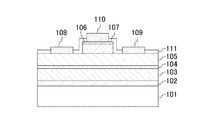
(第1の実施形態)
図1は本発明の第1の実施形態に係る窒化物半導体装置の断面構造の一例を示している。
(First embodiment)
FIG. 1 shows an example of a cross-sectional structure of a nitride semiconductor device according to the first embodiment of the present invention.
図1に示すように、本実施形態の窒化物半導体装置であるトランジスタは、主面の面方位が(0001)面であるサファイア(Al2O3)からなる基板101と、基板101上に形成された膜厚100nmのAlNからなるバッファ層102と、バッファ層102の上に形成された膜厚1μmのアンドープのAlxGa1-xN(但し、xは0<x≦1である。)からなる下地層103と、下地層103の上に形成された膜厚3.5nmのアンドープのGaNからなる第1の半導体層104と、第1の半導体層104の上に形成された膜厚25nmのアンドープのAl0.15Ga0.85Nからなる第2の半導体層105と、第2の半導体層105の上に形成された膜厚100nmのp型Al0.15Ga0.85Nからなるコントロール層106と、コントロール層106の上に形成された膜厚5nmの高濃度のp型GaNからなるコンタクト層107とを有している。
As shown in FIG. 1, the transistor which is the nitride semiconductor device of the present embodiment is formed on a
また、コンタクト層107及びコントロール層106を選択的にエッチングすることにより、コントロール層106及びコンタクト層107からなるコントロール領域が形成され、第2の半導体層105の上で且つコントロール領域の両側方の領域にそれぞれTi及びAlからなるソース電極108並びにドレイン電極109が形成されている。さらに、コンタクト層107の上にニッケル(Ni)からなるゲート電極110が形成されている。また、ソース電極108、ドレイン電極109及びゲート電極110が形成されていない上部表面は、SiNからなるパッシベーション膜111に覆われている。さらに素子分離領域として、例えばホウ素(B)などのイオン注入による高抵抗化層を形成してもよい。
Further, by selectively etching the
コントロール層106には1×1019cm-3程度のマグネシウム(Mg)がドーピングされ、キャリア濃度が1×1018cm-3程度であり、コンタクト層107にはMgが1×1020cm-3程度ドーピングされている。コントロール層106及びコンタクト層107は、基板101の上面からみた場合、例えば1.5μm幅のストライプ状にエッチングされており、その上に幅1μmのゲート電極110が形成されている。
The
本実施形態の窒化物半導体装置において、第2の半導体層105のバンドギャップは第1の半導体層104のバンドギャップよりも大きい。第2の半導体層105とコントロール層106とは同一の材料から形成されているため、コントロール層106のバンドギャップは第1の半導体層104のバンドギャップよりも大きい。このとき第1の半導体層104と第2の半導体層105との界面にはヘテロ障壁が形成されており、本窒化物半導体装置の動作時には第1の半導体層104における第2の半導体層105との界面の近傍に2次元電子ガス層からなるチャネル領域が形成される。
In the nitride semiconductor device of this embodiment, the band gap of the
チャネル領域を含む第1の半導体層104の上側にバンドギャップが大きい第2の半導体層105を形成し、下側にチャネル領域に対して価電子帯にポテンシャル障壁を有する下地層103を形成すると、コントロール層106をチャネル領域に対して順方向にバイアスをかけた場合、第1の半導体層104に生じるチャネル領域にホールが注入され、注入されたホールは、散逸されることなく効率的に第1の半導体層104の電子濃度増加に寄与される。
When the
また、十分に大きなドレイン耐圧を実現するため、図1に示されるコントロール層106とドレイン電極109との間の距離は5μm程度かそれ以上としている。また、従来例において説明した通り、ソース電極108及びドレイン電極109は第2の半導体層105に接して形成されているが、トンネル電流を介して第2の半導体層105と第1の半導体層104とのへテロ接合面に形成される2次元電子ガス層と接続されるため良好なオーミック接触となる。ここではさらに良好なオーミック接触を実現するためにソース電極108及びドレイン電極109下方の第2の半導体層105中にn型不純物であるシリコン(Si)を選択的に拡散させた構成としてもよい。
Further, in order to realize a sufficiently large drain breakdown voltage, the distance between the
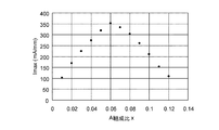
図2は、本発明の第1の実施形態に係る窒化物半導体装置の下地層103を構成するAlの組成比xの値に対する窒化物半導体装置の最大ドレイン電流値との関係(シミュレーション値)を示している。
FIG. 2 shows the relationship (simulation value) of the maximum drain current value of the nitride semiconductor device with respect to the value of the Al composition ratio x constituting the
図2に示されるように、下地層103を構成するAlの組成比xの値は、0.06付近が頂点であり、xが小さくなりすぎても、大きくなりすぎても、窒化物半導体装置の最大ドレイン電流値が小さくなることが示されている。
As shown in FIG. 2, the composition ratio x of Al constituting the
このように、本発明に係る窒化物半導体装置において、チャネル領域(第1の半導体層104)に対して価電子帯にポテンシャル障壁を有するような半導体材料である下地層103を備えた構成とし、下地層103を構成するAlの組成比xの値を0.03以上且つ0.1以下に設定することにより、窒化物半導体装置の最大ドレイン電流値が高い値を達成することができる。
Thus, in the nitride semiconductor device according to the present invention, the
本実施形態においては、基板101の材料としてサファイアを用いたが、サファイアからなる基板に代えて、例えば炭化シリコン(SiC)、GaN又はSi等の材料からなる基板でよく、また良好な結晶性を実現できるのであればいかなる面方位でもよい。なお、ゲート電極110の材料は、Niに代えてコンタクト層107と良好なオーミック接触を有する材料であればPdなどの金属でもよい。また、本実施形態ではコントロール層106及び第2の半導体層105のAl組成が一致しているが、組成を揃える必要はなく、例えばコントロール層にp型GaNを用いてもよい。
In this embodiment, sapphire is used as the material of the
このように、本発明に係る窒化物半導体装置であるトランジスタによると、チャネル層である第1の半導体層の下部に第1の半導体層に対して価電子帯にポテンシャル障壁を有する下地層103を形成し、下地層103を構成するAlの組成比を適切な値に設定することにより、ノーマリオフ型で前述のホール注入によってのみドレイン電流が流れ、ホールのチャネル内での閉じ込めを促進することにより大きな動作電流を実現することが可能となる。
Thus, according to the transistor which is a nitride semiconductor device according to the present invention, the
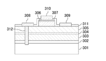
(第2の実施形態)
図3は本発明の第2の実施形態に係る窒化物半導体装置の断面構造の一例を示している。
(Second Embodiment)
FIG. 3 shows an example of a cross-sectional structure of a nitride semiconductor device according to the second embodiment of the present invention.
図3に示すように、本実施形態の窒化物半導体装置であるトランジスタは、主面の面方位が(111)であるn型Siからなる基板301と、基板301の上に形成された膜厚40nmのAlNからなるバッファ層302と、バッファ層302の上に形成された膜厚1μmのアンドープのAl0.05Ga0.95Nからなる下地層303と、下地層303の上に形成された膜厚3.5nmのアンドープのInyGa1-yN(但し、yは0<y≦1である。)からなる第1の半導体層304と、第1の半導体層304の上に形成された膜厚25nmのアンドープのAl0.15Ga0.85Nからなる第2の半導体層305と、第2の半導体層305の上に形成された膜厚100nmのp型Al0.15Ga0.85Nからなるコントロール層306と、コントロール層306の上に形成された膜厚5nmの高濃度のp型GaNからなるコンタクト層307とを有している。
As shown in FIG. 3, the transistor which is the nitride semiconductor device of this embodiment includes a
また、コンタクト層307及びコントロール層306を選択的にエッチングすることにより、コントロール層306及びコンタクト層307からなるコントロール領域が形成され、第2の半導体層305の上で且つコントロール領域の両側方の領域にそれぞれTi及びAlからなるソース電極308並びにドレイン電極309が形成されている。さらに、コンタクト層307上には、Niからなるゲート電極310が形成されている。また、ソース電極308、ドレイン電極309及びゲート電極310が形成されていない上部表面は、SiNからなるパッシベーション膜311に覆われている。また、ソース電極308は、コントロール領域以外の電極の配線抵抗を低減させるため、基板301まで延びる貫通穴312を介して接続されるソースビア構造を有している。
Further, by selectively etching the
本実施形態の窒化物半導体装置は第1の実施形態と同様に、下地層303が、第1の半導体層304に対して価電子帯にポテンシャル障壁を有しており、コントロール領域のバンドギャップはチャネル領域のバンドギャップよりも大きい。
In the nitride semiconductor device of this embodiment, the
図4は本発明の第2の実施形態に係る窒化物半導体装置の第1の半導体層304を構成するInの組成比yの値と窒化物半導体装置の最大ドレイン電流特性(シミュレーション値)との関係を示している。
FIG. 4 shows the composition ratio y of In constituting the
図4に示されるように、第1の半導体層304を構成するInの組成比yの値が大きくなるに従って、窒化物半導体装置の最大ドレイン電流値が増加している。
As shown in FIG. 4, the maximum drain current value of the nitride semiconductor device increases as the value of the In composition ratio y constituting the
このように、本発明に係る窒化物半導体装置は、第1の半導体層304に対して価電子帯にポテンシャル障壁を有するような半導体材料からなる下地層303を備えた構成とし、第1の半導体層304にInを含む構成とすることによりチャネル領域のバンドギャップが小さくなり、電子もホールもチャネル領域により多く蓄積することが可能になる。また、チャネル領域のInの組成比yの値を大きくすることにより、より高い最大ドレイン電流値を達成することができる。
As described above, the nitride semiconductor device according to the present invention includes the
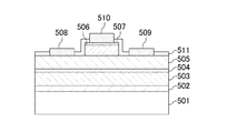
(第3の実施形態)
図5は本発明の第3の実施形態に係る窒化物半導体装置の断面構造の一例を示している。
(Third embodiment)
FIG. 5 shows an example of a cross-sectional structure of a nitride semiconductor device according to the third embodiment of the present invention.
図5に示すように、本実施形態の窒化物半導体装置であるトランジスタは、主面の面方位が(0001)であるサファイアからなる基板501と、基板501の上に形成された膜厚100nmのAlNからなるバッファ層502と、バッファ層502の上に形成された膜厚1μmのアンドープのAl0.05Ga0.95Nからなる下地層503と、下地層503の上に形成された膜厚3.5nmのアンドープのGaNからなる第1の半導体層504と、第1の半導体層504の上に形成された膜厚25nmのアンドープのAl0.15Ga0.85Nからなる第2の半導体層505と、第2の半導体層505の上に形成された膜厚100nmのp型Al0.15Ga0.85Nからなるコントロール層506と、コントロール層506の上に形成された膜厚5nmの高濃度のp型GaNからなるコンタクト層507とを有している。
As shown in FIG. 5, the transistor which is the nitride semiconductor device of this embodiment includes a
また、コンタクト層507及びコントロール層506を選択的にエッチングすることにより、コントロール層506及びコンタクト層507からなるコントロール領域が形成され、第2の半導体層505の上で且つコントロール領域の両側方の領域にそれぞれTi及びAlからなるソース電極508並びにドレイン電極509が形成されている。さらに、コンタクト層507上に、Niからなるゲート電極510が形成されている。また、ソース電極508、ドレイン電極509及びゲート電極510が形成されていない上部表面は、SiNからなるパッシベーション膜511に覆われている。
Further, by selectively etching the
本実施形態の窒化物半導体装置も第1の実施形態と同様に、下地層503が、第1の半導体層504に対して価電子帯にポテンシャル障壁を有しており、コントロール領域のバンドギャップは第1の半導体層504のバンドギャップよりも大きい。
Similarly to the first embodiment, the nitride semiconductor device of the present embodiment has the
図6は、本実施形態に係る窒化物半導体装置の一例であるトランジスタの第1の半導体層504の厚さとスイッチング速度との関係を示している。
FIG. 6 shows the relationship between the thickness of the
図6に示されるように、第1の半導体層504の厚さが厚くなるに従って、スイッチング速度が遅くなる。
As shown in FIG. 6, as the thickness of the
このように、本発明に係る窒化物半導体装置において、チャネル層を構成する第1の半導体層504に対して価電子帯にポテンシャル障壁を有する半導体からなる下地層503を備えた構成とし、第1の半導体層504の厚さを適切な値に設定することにより、高速なスイッチングを行うことが可能となる。このため、ノーマリオフ型で動作電流が大きく且つリーク電流が小さく、スイッチング速度が速い窒化物半導体トランジスタを実現することが可能となる。
Thus, in the nitride semiconductor device according to the present invention, the
本発明に係る窒化物半導体装置は、ノーマリオフ型で動作電流を大きくでき且つ高速スイッチングを行うことが可能な窒化物半導体装置等に有用である。 The nitride semiconductor device according to the present invention is useful for a nitride semiconductor device or the like that is normally-off type and can increase operating current and perform high-speed switching.
101 基板
102 バッファ層
103 下地層
104 第1の半導体層
105 第2の半導体層
106 コントロール層
107 コンタクト層
108 ソース電極
109 ドレイン電極
110 ゲート電極
111 パッシベーション膜
301 基板
302 バッファ層
303 下地層
304 第1の半導体層
305 第2の半導体層
306 コントロール層
307 コンタクト層
308 ソース電極
309 ドレイン電極
310 ゲート電極
311 パッシベーション膜
312 貫通穴
501 基板
502 バッファ層
503 下地層
504 第1の半導体層
505 第2の半導体層
506 コントロール層
507 コンタクト層
508 ソース電極
509 ドレイン電極
510 ゲート電極
511 パッシベーション膜
701 基板
702 アンドープGaN層
703 アンドープAl0.25Ga0.75N層
704 ソース電極
705 ドレイン電極
706 ゲート電極
707 パッシベーション膜
901 基板
902 AlNバッファ層
903 アンドープGaN層
904 アンドープAlGaN層
905 p型コントロール層
906 p型コンタクト層
907 ゲート電極
908 ソース電極
909 ドレイン電極
910 パッシベーション膜
101
Claims (6)
前記第1の半導体層の主面上に形成され、バンドギャップが前記第1の窒化物半導体よりも大きい第2の窒化物半導体からなる第2の半導体層と、
前記第2の半導体層の上部又は上側に選択的に形成され、p型の導電性を有する第3の窒化物半導体からなるコントロール層と、
前記第2の半導体層の上で且つ前記コントロール層の両測方の領域にそれぞれ形成されたソース電極及びドレイン電極と、
前記コントロール層の上側に形成されたゲート電極と、
前記第1の半導体層の前記主面と反対側の面上に形成され、前記第1の窒化物半導体に対して価電子帯にポテンシャル障壁を有し、組成にアルミニウムを含む第4の窒化物半導体からなる第4の半導体層とを備えていることを特徴とする窒化物半導体装置。 A first semiconductor layer made of a first nitride semiconductor;
A second semiconductor layer formed on the main surface of the first semiconductor layer and made of a second nitride semiconductor having a band gap larger than that of the first nitride semiconductor;
A control layer made of a third nitride semiconductor selectively formed on or above the second semiconductor layer and having p-type conductivity;
A source electrode and a drain electrode respectively formed on the second semiconductor layer and in both measurement regions of the control layer;
A gate electrode formed on the control layer;
A fourth nitride formed on a surface opposite to the main surface of the first semiconductor layer, having a potential barrier in a valence band with respect to the first nitride semiconductor, and containing aluminum in the composition A nitride semiconductor device comprising: a fourth semiconductor layer made of a semiconductor.
前記第1の半導体層は、厚さが0nmより大きく且つ30nm以下であることを特徴とする請求項3に記載の窒化物半導体装置。 The first nitride semiconductor contains indium in its composition,
The nitride semiconductor device according to claim 3, wherein the first semiconductor layer has a thickness greater than 0 nm and not greater than 30 nm.
Priority Applications (5)
| Application Number | Priority Date | Filing Date | Title |
|---|---|---|---|
| JP2006016622A JP4705481B2 (en) | 2006-01-25 | 2006-01-25 | Nitride semiconductor device |
| CNA2006101659295A CN101009324A (en) | 2006-01-25 | 2006-12-11 | Nitride semiconductor device |
| CN2011101620703A CN102244097A (en) | 2006-01-25 | 2006-12-11 | Nitride semiconductor device |
| US11/647,218 US7825434B2 (en) | 2006-01-25 | 2006-12-29 | Nitride semiconductor device |
| US12/879,565 US20100327320A1 (en) | 2006-01-25 | 2010-09-10 | Nitride semiconductor device |
Applications Claiming Priority (1)
| Application Number | Priority Date | Filing Date | Title |
|---|---|---|---|
| JP2006016622A JP4705481B2 (en) | 2006-01-25 | 2006-01-25 | Nitride semiconductor device |
Publications (2)
| Publication Number | Publication Date |
|---|---|
| JP2007201093A true JP2007201093A (en) | 2007-08-09 |
| JP4705481B2 JP4705481B2 (en) | 2011-06-22 |
Family
ID=38284671
Family Applications (1)
| Application Number | Title | Priority Date | Filing Date |
|---|---|---|---|
| JP2006016622A Active JP4705481B2 (en) | 2006-01-25 | 2006-01-25 | Nitride semiconductor device |
Country Status (3)
| Country | Link |
|---|---|
| US (2) | US7825434B2 (en) |
| JP (1) | JP4705481B2 (en) |
| CN (2) | CN102244097A (en) |
Cited By (4)
| Publication number | Priority date | Publication date | Assignee | Title |
|---|---|---|---|---|
| JP2010539712A (en) * | 2007-09-12 | 2010-12-16 | トランスフォーム インコーポレイテッド | III-nitride bidirectional switch |
| JP2012019186A (en) * | 2010-07-07 | 2012-01-26 | Samsung Electro-Mechanics Co Ltd | Nitride-based semiconductor device and method for manufacturing the same |
| JP2014146744A (en) * | 2013-01-30 | 2014-08-14 | Renesas Electronics Corp | Semiconductor device |
| WO2018181237A1 (en) | 2017-03-31 | 2018-10-04 | パナソニックIpマネジメント株式会社 | Semiconductor device |
Families Citing this family (16)
| Publication number | Priority date | Publication date | Assignee | Title |
|---|---|---|---|---|
| US7531854B2 (en) | 2007-05-04 | 2009-05-12 | Dsm Solutions, Inc. | Semiconductor device having strain-inducing substrate and fabrication methods thereof |
| US7772056B2 (en) * | 2007-06-18 | 2010-08-10 | University Of Utah Research Foundation | Transistors for replacing metal-oxide semiconductor field-effect transistors in nanoelectronics |
| JP4478175B2 (en) * | 2007-06-26 | 2010-06-09 | 株式会社東芝 | Semiconductor device |
| JP2009200395A (en) * | 2008-02-25 | 2009-09-03 | Sanken Electric Co Ltd | Hfet, and manufacturing method thereof |
| JP2009231508A (en) * | 2008-03-21 | 2009-10-08 | Panasonic Corp | Semiconductor device |
| EP2166085A1 (en) * | 2008-07-16 | 2010-03-24 | Suomen Punainen Risti Veripalvelu | Divalent modified cells |
| JP5595685B2 (en) * | 2009-07-28 | 2014-09-24 | パナソニック株式会社 | Semiconductor device |
| US9378965B2 (en) * | 2009-12-10 | 2016-06-28 | Infineon Technologies Americas Corp. | Highly conductive source/drain contacts in III-nitride transistors |
| JP2011233751A (en) * | 2010-04-28 | 2011-11-17 | Panasonic Corp | Nitride semiconductor transistor |
| JP5576731B2 (en) * | 2010-07-14 | 2014-08-20 | パナソニック株式会社 | Field effect transistor |
| US8946788B2 (en) * | 2011-08-04 | 2015-02-03 | Avogy, Inc. | Method and system for doping control in gallium nitride based devices |
| CN108807526B (en) * | 2012-04-20 | 2021-12-21 | 苏州晶湛半导体有限公司 | Enhanced switching device and method of making same |
| JP2014072427A (en) * | 2012-09-28 | 2014-04-21 | Fujitsu Ltd | Semiconductor device and semiconductor device manufacturing method |
| JP6189235B2 (en) * | 2014-03-14 | 2017-08-30 | 株式会社東芝 | Semiconductor device |
| JP6642883B2 (en) * | 2015-10-08 | 2020-02-12 | ローム株式会社 | Nitride semiconductor device and method of manufacturing the same |
| CN112928161B (en) * | 2019-12-06 | 2024-01-02 | 联华电子股份有限公司 | High electron mobility transistor and manufacturing method thereof |
Citations (5)
| Publication number | Priority date | Publication date | Assignee | Title |
|---|---|---|---|---|
| JPS61230381A (en) * | 1985-04-05 | 1986-10-14 | Nec Corp | Semiconductor device |
| JPH02177332A (en) * | 1988-12-27 | 1990-07-10 | Nec Corp | Semiconductor device |
| JPH11261053A (en) * | 1998-03-09 | 1999-09-24 | Furukawa Electric Co Ltd:The | High electron mobility transistor |
| JP2000299325A (en) * | 1999-04-16 | 2000-10-24 | Hitachi Cable Ltd | Epitaxial wafer for field effect transistor using gallium nitride compound semiconductor |
| JP2001196575A (en) * | 2000-01-13 | 2001-07-19 | Matsushita Electric Ind Co Ltd | Semiconductor device |
Family Cites Families (11)
| Publication number | Priority date | Publication date | Assignee | Title |
|---|---|---|---|---|
| EP0200933B1 (en) * | 1985-04-05 | 1992-11-04 | Nec Corporation | Heterojunction transistor having bipolar characteristics |
| JP3716906B2 (en) * | 2000-03-06 | 2005-11-16 | 日本電気株式会社 | Field effect transistor |
| JP4906023B2 (en) * | 2001-08-14 | 2012-03-28 | 古河電気工業株式会社 | GaN-based semiconductor device |
| US7030428B2 (en) * | 2001-12-03 | 2006-04-18 | Cree, Inc. | Strain balanced nitride heterojunction transistors |
| JP3986887B2 (en) * | 2002-05-17 | 2007-10-03 | 松下電器産業株式会社 | Semiconductor device |
| JP2004273486A (en) | 2003-03-05 | 2004-09-30 | Mitsubishi Electric Corp | Semiconductor device and its manufacturing method |
| US7098490B2 (en) * | 2003-06-02 | 2006-08-29 | Hrl Laboratories, Llc | GaN DHFET |
| US7382001B2 (en) * | 2004-01-23 | 2008-06-03 | International Rectifier Corporation | Enhancement mode III-nitride FET |
| JP4041075B2 (en) * | 2004-02-27 | 2008-01-30 | 株式会社東芝 | Semiconductor device |
| JP4705412B2 (en) * | 2005-06-06 | 2011-06-22 | パナソニック株式会社 | Field effect transistor and manufacturing method thereof |
| JP4712459B2 (en) * | 2005-07-08 | 2011-06-29 | パナソニック株式会社 | Transistor and method of operating the same |
-
2006
- 2006-01-25 JP JP2006016622A patent/JP4705481B2/en active Active
- 2006-12-11 CN CN2011101620703A patent/CN102244097A/en active Pending
- 2006-12-11 CN CNA2006101659295A patent/CN101009324A/en active Pending
- 2006-12-29 US US11/647,218 patent/US7825434B2/en active Active
-
2010
- 2010-09-10 US US12/879,565 patent/US20100327320A1/en not_active Abandoned
Patent Citations (5)
| Publication number | Priority date | Publication date | Assignee | Title |
|---|---|---|---|---|
| JPS61230381A (en) * | 1985-04-05 | 1986-10-14 | Nec Corp | Semiconductor device |
| JPH02177332A (en) * | 1988-12-27 | 1990-07-10 | Nec Corp | Semiconductor device |
| JPH11261053A (en) * | 1998-03-09 | 1999-09-24 | Furukawa Electric Co Ltd:The | High electron mobility transistor |
| JP2000299325A (en) * | 1999-04-16 | 2000-10-24 | Hitachi Cable Ltd | Epitaxial wafer for field effect transistor using gallium nitride compound semiconductor |
| JP2001196575A (en) * | 2000-01-13 | 2001-07-19 | Matsushita Electric Ind Co Ltd | Semiconductor device |
Cited By (5)
| Publication number | Priority date | Publication date | Assignee | Title |
|---|---|---|---|---|
| JP2010539712A (en) * | 2007-09-12 | 2010-12-16 | トランスフォーム インコーポレイテッド | III-nitride bidirectional switch |
| JP2012019186A (en) * | 2010-07-07 | 2012-01-26 | Samsung Electro-Mechanics Co Ltd | Nitride-based semiconductor device and method for manufacturing the same |
| JP2014146744A (en) * | 2013-01-30 | 2014-08-14 | Renesas Electronics Corp | Semiconductor device |
| US9768257B2 (en) | 2013-01-30 | 2017-09-19 | Renesas Electronics Corporation | Semiconductor device |
| WO2018181237A1 (en) | 2017-03-31 | 2018-10-04 | パナソニックIpマネジメント株式会社 | Semiconductor device |
Also Published As
| Publication number | Publication date |
|---|---|
| CN101009324A (en) | 2007-08-01 |
| JP4705481B2 (en) | 2011-06-22 |
| US20100327320A1 (en) | 2010-12-30 |
| US7825434B2 (en) | 2010-11-02 |
| CN102244097A (en) | 2011-11-16 |
| US20070170463A1 (en) | 2007-07-26 |
Similar Documents
| Publication | Publication Date | Title |
|---|---|---|
| JP4705481B2 (en) | Nitride semiconductor device | |
| JP4712459B2 (en) | Transistor and method of operating the same | |
| JP5147197B2 (en) | Transistor | |
| US8779438B2 (en) | Field-effect transistor with nitride semiconductor and method for fabricating the same | |
| US8390029B2 (en) | Semiconductor device for reducing and/or preventing current collapse | |
| JP6371986B2 (en) | Nitride semiconductor structure | |
| JP6229172B2 (en) | Semiconductor device | |
| EP2747145B1 (en) | Field-effect transistor | |
| US20140110759A1 (en) | Semiconductor device | |
| WO2010064383A1 (en) | Field effect transistor and method for manufacturing same | |
| JP2008091392A (en) | Nitride semiconductor device, and its manufacturing method | |
| JP5691138B2 (en) | Field effect transistor and manufacturing method thereof | |
| JP2008130655A (en) | Semiconductor element | |
| JP2011029507A (en) | Semiconductor device | |
| JP2012227456A (en) | Semiconductor device | |
| JP2011142358A (en) | Nitride semiconductor device | |
| JP2011066464A (en) | Field effect transistor | |
| JP2013239735A (en) | Field effect transistor | |
| JP5721782B2 (en) | Semiconductor device | |
| JP2015056413A (en) | Nitride semiconductor device |
Legal Events
| Date | Code | Title | Description |
|---|---|---|---|
| A621 | Written request for application examination |
Free format text: JAPANESE INTERMEDIATE CODE: A621 Effective date: 20080630 |
|
| A131 | Notification of reasons for refusal |
Free format text: JAPANESE INTERMEDIATE CODE: A131 Effective date: 20101116 |
|
| A521 | Written amendment |
Free format text: JAPANESE INTERMEDIATE CODE: A523 Effective date: 20101224 |
|
| TRDD | Decision of grant or rejection written | ||
| A01 | Written decision to grant a patent or to grant a registration (utility model) |
Free format text: JAPANESE INTERMEDIATE CODE: A01 Effective date: 20110215 |
|
| A61 | First payment of annual fees (during grant procedure) |
Free format text: JAPANESE INTERMEDIATE CODE: A61 Effective date: 20110311 |
|
| R150 | Certificate of patent or registration of utility model |
Ref document number: 4705481 Country of ref document: JP Free format text: JAPANESE INTERMEDIATE CODE: R150 |