JP2007178311A - プローブ - Google Patents
プローブ Download PDFInfo
- Publication number
- JP2007178311A JP2007178311A JP2005378224A JP2005378224A JP2007178311A JP 2007178311 A JP2007178311 A JP 2007178311A JP 2005378224 A JP2005378224 A JP 2005378224A JP 2005378224 A JP2005378224 A JP 2005378224A JP 2007178311 A JP2007178311 A JP 2007178311A
- Authority
- JP
- Japan
- Prior art keywords
- probe
- measurement
- contact
- current
- voltage
- Prior art date
- Legal status (The legal status is an assumption and is not a legal conclusion. Google has not performed a legal analysis and makes no representation as to the accuracy of the status listed.)
- Pending
Links
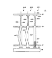
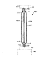
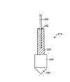
- 239000000523 sample Substances 0.000 title claims abstract description 566
- 238000005259 measurement Methods 0.000 claims abstract description 206
- 238000004519 manufacturing process Methods 0.000 claims abstract description 13
- 239000000758 substrate Substances 0.000 claims description 17
- 238000012545 processing Methods 0.000 claims description 9
- 238000007689 inspection Methods 0.000 claims description 5
- 238000005452 bending Methods 0.000 claims description 3
- 238000000034 method Methods 0.000 claims description 3
- 230000006835 compression Effects 0.000 claims 2
- 238000007906 compression Methods 0.000 claims 2
- 238000000691 measurement method Methods 0.000 description 4
- 238000010586 diagram Methods 0.000 description 3
- 238000003825 pressing Methods 0.000 description 3
- RYGMFSIKBFXOCR-UHFFFAOYSA-N Copper Chemical compound [Cu] RYGMFSIKBFXOCR-UHFFFAOYSA-N 0.000 description 2
- 239000004020 conductor Substances 0.000 description 2
- 229910052802 copper Inorganic materials 0.000 description 2
- 239000010949 copper Substances 0.000 description 2
- 238000009413 insulation Methods 0.000 description 2
- 239000004065 semiconductor Substances 0.000 description 2
- 229910000679 solder Inorganic materials 0.000 description 2
- 238000012360 testing method Methods 0.000 description 2
- 238000007792 addition Methods 0.000 description 1
- 239000011248 coating agent Substances 0.000 description 1
- 238000000576 coating method Methods 0.000 description 1
- 238000012217 deletion Methods 0.000 description 1
- 230000037430 deletion Effects 0.000 description 1
- 238000010030 laminating Methods 0.000 description 1
- 239000004973 liquid crystal related substance Substances 0.000 description 1
- 239000000463 material Substances 0.000 description 1
- 238000012986 modification Methods 0.000 description 1
- 230000004048 modification Effects 0.000 description 1
Images


Landscapes
- Testing Of Individual Semiconductor Devices (AREA)
- Measuring Leads Or Probes (AREA)
Priority Applications (1)
| Application Number | Priority Date | Filing Date | Title |
|---|---|---|---|
| JP2005378224A JP2007178311A (ja) | 2005-12-28 | 2005-12-28 | プローブ |
Applications Claiming Priority (1)
| Application Number | Priority Date | Filing Date | Title |
|---|---|---|---|
| JP2005378224A JP2007178311A (ja) | 2005-12-28 | 2005-12-28 | プローブ |
Publications (2)
| Publication Number | Publication Date |
|---|---|
| JP2007178311A true JP2007178311A (ja) | 2007-07-12 |
| JP2007178311A5 JP2007178311A5 (enExample) | 2009-02-12 |
Family
ID=38303641
Family Applications (1)
| Application Number | Title | Priority Date | Filing Date |
|---|---|---|---|
| JP2005378224A Pending JP2007178311A (ja) | 2005-12-28 | 2005-12-28 | プローブ |
Country Status (1)
| Country | Link |
|---|---|
| JP (1) | JP2007178311A (enExample) |
Cited By (3)
| Publication number | Priority date | Publication date | Assignee | Title |
|---|---|---|---|---|
| JP2012083234A (ja) * | 2010-10-13 | 2012-04-26 | Hioki Ee Corp | プローブおよび測定装置 |
| KR101807503B1 (ko) | 2016-09-28 | 2017-12-11 | 경성대학교 산학협력단 | 콘크리트의 표면비저항 측정 장치의 전극 홀더 및 이 전극 홀더를 포함하는 측정 장치 |
| JPWO2022176341A1 (enExample) * | 2021-02-17 | 2022-08-25 |
-
2005
- 2005-12-28 JP JP2005378224A patent/JP2007178311A/ja active Pending
Cited By (5)
| Publication number | Priority date | Publication date | Assignee | Title |
|---|---|---|---|---|
| JP2012083234A (ja) * | 2010-10-13 | 2012-04-26 | Hioki Ee Corp | プローブおよび測定装置 |
| KR101807503B1 (ko) | 2016-09-28 | 2017-12-11 | 경성대학교 산학협력단 | 콘크리트의 표면비저항 측정 장치의 전극 홀더 및 이 전극 홀더를 포함하는 측정 장치 |
| JPWO2022176341A1 (enExample) * | 2021-02-17 | 2022-08-25 | ||
| WO2022176341A1 (ja) * | 2021-02-17 | 2022-08-25 | パナソニックIpマネジメント株式会社 | デバイス、デバイス製造装置、及びデバイス製造方法 |
| JP7766265B2 (ja) | 2021-02-17 | 2025-11-10 | パナソニックIpマネジメント株式会社 | デバイス、デバイス製造装置、及びデバイス製造方法 |
Similar Documents
| Publication | Publication Date | Title |
|---|---|---|
| JP6116903B2 (ja) | コンタクトプローブおよびプローブユニット | |
| JP6109072B2 (ja) | プローブユニット | |
| JP6255914B2 (ja) | 検査治具 | |
| US10649005B2 (en) | Contact terminal, inspection jig, and inspection device | |
| JP2010281583A (ja) | 検査用治具 | |
| JP5776687B2 (ja) | 検査用接触子及び検査用治具 | |
| JP6858945B2 (ja) | 検査治具、検査装置、及びプローブ | |
| KR100975808B1 (ko) | 기판검사용 치구 | |
| JP2014025737A (ja) | 検査用治具及び接触子 | |
| JP2010276510A (ja) | 検査用治具 | |
| WO2012108066A1 (ja) | 検査治具 | |
| JP2010281592A (ja) | プローブ及び検査用治具 | |
| JP5070956B2 (ja) | 基板検査用接触子及び基板検査用治具 | |
| JPWO2020145073A1 (ja) | 接触端子、検査治具、及び検査装置 | |
| JP2007178318A (ja) | 基板検査装置及び方法 | |
| TWI427297B (zh) | 基板檢查用之檢查治具 | |
| WO2017208690A1 (ja) | 接触導電治具、及び検査装置 | |
| JP2011137663A (ja) | 検査用治具、検査用治具の接続体及びその製造方法 | |
| JP5088504B2 (ja) | 基板検査用接触子及びその製造方法 | |
| JP2007194187A (ja) | コンタクトピン、及び電気部品用ソケット | |
| JP2007178311A (ja) | プローブ | |
| JP5062355B2 (ja) | 接続端子及び接続端子の製造方法 | |
| JP5540971B2 (ja) | 接触子、接続治具及び接触子の製造方法 | |
| JP5282873B2 (ja) | 基板検査用の一対のプローブ及び基板検査用治具 | |
| JP2003347370A (ja) | 半導体ウエーハの評価装置及び評価方法 |
Legal Events
| Date | Code | Title | Description |
|---|---|---|---|
| A521 | Request for written amendment filed |
Free format text: JAPANESE INTERMEDIATE CODE: A523 Effective date: 20081218 |
|
| A621 | Written request for application examination |
Free format text: JAPANESE INTERMEDIATE CODE: A621 Effective date: 20081218 |
|
| A871 | Explanation of circumstances concerning accelerated examination |
Free format text: JAPANESE INTERMEDIATE CODE: A871 Effective date: 20081218 |
|
| A975 | Report on accelerated examination |
Free format text: JAPANESE INTERMEDIATE CODE: A971005 Effective date: 20090116 |
|
| A131 | Notification of reasons for refusal |
Free format text: JAPANESE INTERMEDIATE CODE: A131 Effective date: 20090120 |
|
| A521 | Request for written amendment filed |
Free format text: JAPANESE INTERMEDIATE CODE: A523 Effective date: 20090317 |
|
| A131 | Notification of reasons for refusal |
Free format text: JAPANESE INTERMEDIATE CODE: A131 Effective date: 20090407 |
|
| A02 | Decision of refusal |
Free format text: JAPANESE INTERMEDIATE CODE: A02 Effective date: 20091020 |