JP2007141903A - 半導体装置およびその製造方法 - Google Patents
半導体装置およびその製造方法 Download PDFInfo
- Publication number
- JP2007141903A JP2007141903A JP2005329593A JP2005329593A JP2007141903A JP 2007141903 A JP2007141903 A JP 2007141903A JP 2005329593 A JP2005329593 A JP 2005329593A JP 2005329593 A JP2005329593 A JP 2005329593A JP 2007141903 A JP2007141903 A JP 2007141903A
- Authority
- JP
- Japan
- Prior art keywords
- silicon nitride
- nitride film
- gate electrode
- misfet
- silicon
- Prior art date
- Legal status (The legal status is an assumption and is not a legal conclusion. Google has not performed a legal analysis and makes no representation as to the accuracy of the status listed.)
- Withdrawn
Links
- 239000004065 semiconductor Substances 0.000 title claims abstract description 66
- 238000004519 manufacturing process Methods 0.000 title claims description 25
- 229910052581 Si3N4 Inorganic materials 0.000 claims abstract description 140
- HQVNEWCFYHHQES-UHFFFAOYSA-N silicon nitride Chemical compound N12[Si]34N5[Si]62N3[Si]51N64 HQVNEWCFYHHQES-UHFFFAOYSA-N 0.000 claims abstract description 140
- 239000000758 substrate Substances 0.000 claims abstract description 26
- XUIMIQQOPSSXEZ-UHFFFAOYSA-N Silicon Chemical compound [Si] XUIMIQQOPSSXEZ-UHFFFAOYSA-N 0.000 claims description 66
- 229910052710 silicon Inorganic materials 0.000 claims description 66
- 239000010703 silicon Substances 0.000 claims description 66
- 238000000034 method Methods 0.000 claims description 52
- 230000008569 process Effects 0.000 claims description 19
- 229910052751 metal Inorganic materials 0.000 claims description 18
- 239000002184 metal Substances 0.000 claims description 18
- 230000005669 field effect Effects 0.000 claims description 5
- 239000012212 insulator Substances 0.000 claims description 5
- 229910021420 polycrystalline silicon Inorganic materials 0.000 abstract description 28
- 229920005591 polysilicon Polymers 0.000 abstract description 28
- VYPSYNLAJGMNEJ-UHFFFAOYSA-N Silicium dioxide Chemical compound O=[Si]=O VYPSYNLAJGMNEJ-UHFFFAOYSA-N 0.000 abstract description 12
- 229910052814 silicon oxide Inorganic materials 0.000 abstract description 12
- 230000015572 biosynthetic process Effects 0.000 abstract description 7
- 229910021332 silicide Inorganic materials 0.000 abstract description 5
- FVBUAEGBCNSCDD-UHFFFAOYSA-N silicide(4-) Chemical compound [Si-4] FVBUAEGBCNSCDD-UHFFFAOYSA-N 0.000 abstract description 5
- 238000010586 diagram Methods 0.000 description 12
- 239000012535 impurity Substances 0.000 description 8
- 238000005530 etching Methods 0.000 description 6
- 239000011229 interlayer Substances 0.000 description 5
- 238000005229 chemical vapour deposition Methods 0.000 description 4
- 238000002955 isolation Methods 0.000 description 4
- 239000010410 layer Substances 0.000 description 4
- 238000000206 photolithography Methods 0.000 description 4
- 238000005268 plasma chemical vapour deposition Methods 0.000 description 4
- 229910000449 hafnium oxide Inorganic materials 0.000 description 3
- WIHZLLGSGQNAGK-UHFFFAOYSA-N hafnium(4+);oxygen(2-) Chemical compound [O-2].[O-2].[Hf+4] WIHZLLGSGQNAGK-UHFFFAOYSA-N 0.000 description 3
- 150000002500 ions Chemical class 0.000 description 3
- 239000002356 single layer Substances 0.000 description 3
- 238000010438 heat treatment Methods 0.000 description 2
- 238000005468 ion implantation Methods 0.000 description 2
- 229910052759 nickel Inorganic materials 0.000 description 2
- 230000003071 parasitic effect Effects 0.000 description 2
- 238000001039 wet etching Methods 0.000 description 2
- 229910052787 antimony Inorganic materials 0.000 description 1
- 229910052785 arsenic Inorganic materials 0.000 description 1
- 229910052796 boron Inorganic materials 0.000 description 1
- 239000000969 carrier Substances 0.000 description 1
- 238000006243 chemical reaction Methods 0.000 description 1
- 230000003247 decreasing effect Effects 0.000 description 1
- 238000000151 deposition Methods 0.000 description 1
- 230000003292 diminished effect Effects 0.000 description 1
- 238000001312 dry etching Methods 0.000 description 1
- 230000009977 dual effect Effects 0.000 description 1
- 230000000694 effects Effects 0.000 description 1
- 229910052731 fluorine Inorganic materials 0.000 description 1
- 230000008570 general process Effects 0.000 description 1
- 229910052735 hafnium Inorganic materials 0.000 description 1
- VBJZVLUMGGDVMO-UHFFFAOYSA-N hafnium atom Chemical compound [Hf] VBJZVLUMGGDVMO-UHFFFAOYSA-N 0.000 description 1
- 229910052738 indium Inorganic materials 0.000 description 1
- 239000000463 material Substances 0.000 description 1
- 230000004048 modification Effects 0.000 description 1
- 238000012986 modification Methods 0.000 description 1
- 229910052757 nitrogen Inorganic materials 0.000 description 1
- 230000003647 oxidation Effects 0.000 description 1
- 238000007254 oxidation reaction Methods 0.000 description 1
- 229910052698 phosphorus Inorganic materials 0.000 description 1
- 229910052697 platinum Inorganic materials 0.000 description 1
- 238000005498 polishing Methods 0.000 description 1
- 230000002265 prevention Effects 0.000 description 1
- 239000000126 substance Substances 0.000 description 1
Images


Classifications
-
- H—ELECTRICITY
- H01—ELECTRIC ELEMENTS
- H01L—SEMICONDUCTOR DEVICES NOT COVERED BY CLASS H10
- H01L21/00—Processes or apparatus adapted for the manufacture or treatment of semiconductor or solid state devices or of parts thereof
- H01L21/70—Manufacture or treatment of devices consisting of a plurality of solid state components formed in or on a common substrate or of parts thereof; Manufacture of integrated circuit devices or of parts thereof
- H01L21/77—Manufacture or treatment of devices consisting of a plurality of solid state components or integrated circuits formed in, or on, a common substrate
- H01L21/78—Manufacture or treatment of devices consisting of a plurality of solid state components or integrated circuits formed in, or on, a common substrate with subsequent division of the substrate into plural individual devices
- H01L21/82—Manufacture or treatment of devices consisting of a plurality of solid state components or integrated circuits formed in, or on, a common substrate with subsequent division of the substrate into plural individual devices to produce devices, e.g. integrated circuits, each consisting of a plurality of components
- H01L21/822—Manufacture or treatment of devices consisting of a plurality of solid state components or integrated circuits formed in, or on, a common substrate with subsequent division of the substrate into plural individual devices to produce devices, e.g. integrated circuits, each consisting of a plurality of components the substrate being a semiconductor, using silicon technology
- H01L21/8232—Field-effect technology
- H01L21/8234—MIS technology, i.e. integration processes of field effect transistors of the conductor-insulator-semiconductor type
- H01L21/8238—Complementary field-effect transistors, e.g. CMOS
- H01L21/823807—Complementary field-effect transistors, e.g. CMOS with a particular manufacturing method of the channel structures, e.g. channel implants, halo or pocket implants, or channel materials
-
- H—ELECTRICITY
- H01—ELECTRIC ELEMENTS
- H01L—SEMICONDUCTOR DEVICES NOT COVERED BY CLASS H10
- H01L21/00—Processes or apparatus adapted for the manufacture or treatment of semiconductor or solid state devices or of parts thereof
- H01L21/02—Manufacture or treatment of semiconductor devices or of parts thereof
- H01L21/04—Manufacture or treatment of semiconductor devices or of parts thereof the devices having at least one potential-jump barrier or surface barrier, e.g. PN junction, depletion layer or carrier concentration layer
- H01L21/18—Manufacture or treatment of semiconductor devices or of parts thereof the devices having at least one potential-jump barrier or surface barrier, e.g. PN junction, depletion layer or carrier concentration layer the devices having semiconductor bodies comprising elements of Group IV of the Periodic System or AIIIBV compounds with or without impurities, e.g. doping materials
- H01L21/28—Manufacture of electrodes on semiconductor bodies using processes or apparatus not provided for in groups H01L21/20 - H01L21/268
- H01L21/28008—Making conductor-insulator-semiconductor electrodes
- H01L21/28017—Making conductor-insulator-semiconductor electrodes the insulator being formed after the semiconductor body, the semiconductor being silicon
- H01L21/28026—Making conductor-insulator-semiconductor electrodes the insulator being formed after the semiconductor body, the semiconductor being silicon characterised by the conductor
- H01L21/28097—Making conductor-insulator-semiconductor electrodes the insulator being formed after the semiconductor body, the semiconductor being silicon characterised by the conductor the final conductor layer next to the insulator being a metallic silicide
-
- H—ELECTRICITY
- H01—ELECTRIC ELEMENTS
- H01L—SEMICONDUCTOR DEVICES NOT COVERED BY CLASS H10
- H01L21/00—Processes or apparatus adapted for the manufacture or treatment of semiconductor or solid state devices or of parts thereof
- H01L21/70—Manufacture or treatment of devices consisting of a plurality of solid state components formed in or on a common substrate or of parts thereof; Manufacture of integrated circuit devices or of parts thereof
- H01L21/77—Manufacture or treatment of devices consisting of a plurality of solid state components or integrated circuits formed in, or on, a common substrate
- H01L21/78—Manufacture or treatment of devices consisting of a plurality of solid state components or integrated circuits formed in, or on, a common substrate with subsequent division of the substrate into plural individual devices
- H01L21/82—Manufacture or treatment of devices consisting of a plurality of solid state components or integrated circuits formed in, or on, a common substrate with subsequent division of the substrate into plural individual devices to produce devices, e.g. integrated circuits, each consisting of a plurality of components
- H01L21/822—Manufacture or treatment of devices consisting of a plurality of solid state components or integrated circuits formed in, or on, a common substrate with subsequent division of the substrate into plural individual devices to produce devices, e.g. integrated circuits, each consisting of a plurality of components the substrate being a semiconductor, using silicon technology
- H01L21/8232—Field-effect technology
- H01L21/8234—MIS technology, i.e. integration processes of field effect transistors of the conductor-insulator-semiconductor type
- H01L21/8238—Complementary field-effect transistors, e.g. CMOS
- H01L21/823828—Complementary field-effect transistors, e.g. CMOS with a particular manufacturing method of the gate conductors, e.g. particular materials, shapes
- H01L21/823835—Complementary field-effect transistors, e.g. CMOS with a particular manufacturing method of the gate conductors, e.g. particular materials, shapes silicided or salicided gate conductors
-
- H—ELECTRICITY
- H01—ELECTRIC ELEMENTS
- H01L—SEMICONDUCTOR DEVICES NOT COVERED BY CLASS H10
- H01L21/00—Processes or apparatus adapted for the manufacture or treatment of semiconductor or solid state devices or of parts thereof
- H01L21/70—Manufacture or treatment of devices consisting of a plurality of solid state components formed in or on a common substrate or of parts thereof; Manufacture of integrated circuit devices or of parts thereof
- H01L21/77—Manufacture or treatment of devices consisting of a plurality of solid state components or integrated circuits formed in, or on, a common substrate
- H01L21/78—Manufacture or treatment of devices consisting of a plurality of solid state components or integrated circuits formed in, or on, a common substrate with subsequent division of the substrate into plural individual devices
- H01L21/82—Manufacture or treatment of devices consisting of a plurality of solid state components or integrated circuits formed in, or on, a common substrate with subsequent division of the substrate into plural individual devices to produce devices, e.g. integrated circuits, each consisting of a plurality of components
- H01L21/822—Manufacture or treatment of devices consisting of a plurality of solid state components or integrated circuits formed in, or on, a common substrate with subsequent division of the substrate into plural individual devices to produce devices, e.g. integrated circuits, each consisting of a plurality of components the substrate being a semiconductor, using silicon technology
- H01L21/8232—Field-effect technology
- H01L21/8234—MIS technology, i.e. integration processes of field effect transistors of the conductor-insulator-semiconductor type
- H01L21/8238—Complementary field-effect transistors, e.g. CMOS
- H01L21/823864—Complementary field-effect transistors, e.g. CMOS with a particular manufacturing method of the gate sidewall spacers, e.g. double spacers, particular spacer material or shape
-
- H—ELECTRICITY
- H01—ELECTRIC ELEMENTS
- H01L—SEMICONDUCTOR DEVICES NOT COVERED BY CLASS H10
- H01L29/00—Semiconductor devices adapted for rectifying, amplifying, oscillating or switching, or capacitors or resistors with at least one potential-jump barrier or surface barrier, e.g. PN junction depletion layer or carrier concentration layer; Details of semiconductor bodies or of electrodes thereof ; Multistep manufacturing processes therefor
- H01L29/40—Electrodes ; Multistep manufacturing processes therefor
- H01L29/43—Electrodes ; Multistep manufacturing processes therefor characterised by the materials of which they are formed
- H01L29/49—Metal-insulator-semiconductor electrodes, e.g. gates of MOSFET
- H01L29/4966—Metal-insulator-semiconductor electrodes, e.g. gates of MOSFET the conductor material next to the insulator being a composite material, e.g. organic material, TiN, MoSi2
- H01L29/4975—Metal-insulator-semiconductor electrodes, e.g. gates of MOSFET the conductor material next to the insulator being a composite material, e.g. organic material, TiN, MoSi2 being a silicide layer, e.g. TiSi2
-
- H—ELECTRICITY
- H01—ELECTRIC ELEMENTS
- H01L—SEMICONDUCTOR DEVICES NOT COVERED BY CLASS H10
- H01L29/00—Semiconductor devices adapted for rectifying, amplifying, oscillating or switching, or capacitors or resistors with at least one potential-jump barrier or surface barrier, e.g. PN junction depletion layer or carrier concentration layer; Details of semiconductor bodies or of electrodes thereof ; Multistep manufacturing processes therefor
- H01L29/66—Types of semiconductor device ; Multistep manufacturing processes therefor
- H01L29/66007—Multistep manufacturing processes
- H01L29/66075—Multistep manufacturing processes of devices having semiconductor bodies comprising group 14 or group 13/15 materials
- H01L29/66227—Multistep manufacturing processes of devices having semiconductor bodies comprising group 14 or group 13/15 materials the devices being controllable only by the electric current supplied or the electric potential applied, to an electrode which does not carry the current to be rectified, amplified or switched, e.g. three-terminal devices
- H01L29/66409—Unipolar field-effect transistors
- H01L29/66477—Unipolar field-effect transistors with an insulated gate, i.e. MISFET
- H01L29/665—Unipolar field-effect transistors with an insulated gate, i.e. MISFET using self aligned silicidation, i.e. salicide
-
- H—ELECTRICITY
- H01—ELECTRIC ELEMENTS
- H01L—SEMICONDUCTOR DEVICES NOT COVERED BY CLASS H10
- H01L29/00—Semiconductor devices adapted for rectifying, amplifying, oscillating or switching, or capacitors or resistors with at least one potential-jump barrier or surface barrier, e.g. PN junction depletion layer or carrier concentration layer; Details of semiconductor bodies or of electrodes thereof ; Multistep manufacturing processes therefor
- H01L29/66—Types of semiconductor device ; Multistep manufacturing processes therefor
- H01L29/68—Types of semiconductor device ; Multistep manufacturing processes therefor controllable by only the electric current supplied, or only the electric potential applied, to an electrode which does not carry the current to be rectified, amplified or switched
- H01L29/76—Unipolar devices, e.g. field effect transistors
- H01L29/772—Field effect transistors
- H01L29/78—Field effect transistors with field effect produced by an insulated gate
- H01L29/7842—Field effect transistors with field effect produced by an insulated gate means for exerting mechanical stress on the crystal lattice of the channel region, e.g. using a flexible substrate
- H01L29/7843—Field effect transistors with field effect produced by an insulated gate means for exerting mechanical stress on the crystal lattice of the channel region, e.g. using a flexible substrate the means being an applied insulating layer
-
- H—ELECTRICITY
- H01—ELECTRIC ELEMENTS
- H01L—SEMICONDUCTOR DEVICES NOT COVERED BY CLASS H10
- H01L29/00—Semiconductor devices adapted for rectifying, amplifying, oscillating or switching, or capacitors or resistors with at least one potential-jump barrier or surface barrier, e.g. PN junction depletion layer or carrier concentration layer; Details of semiconductor bodies or of electrodes thereof ; Multistep manufacturing processes therefor
- H01L29/40—Electrodes ; Multistep manufacturing processes therefor
- H01L29/43—Electrodes ; Multistep manufacturing processes therefor characterised by the materials of which they are formed
- H01L29/49—Metal-insulator-semiconductor electrodes, e.g. gates of MOSFET
- H01L29/51—Insulating materials associated therewith
- H01L29/517—Insulating materials associated therewith the insulating material comprising a metallic compound, e.g. metal oxide, metal silicate
Abstract
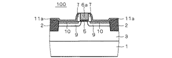
【解決手段】MISFET形成済みの半導体基板上に第1のライナーシリコン窒化膜11aを形成し、ゲート電極6の側方を十分に充填するよう、第1のライナーシリコン窒化膜11a上にシリコン酸化膜等の絶縁膜を形成する。次に、絶縁膜および第1のライナーシリコン窒化膜11aに平坦化処理を施して、ポリシリコンゲート電極6aを露出させ、第1のライナーシリコン窒化膜11aを残置しつつ絶縁膜を除去する。露出したゲート電極6をフルシリサイド化し、第1のライナーシリコン窒化膜11aおよび露出したフルシリサイド化ゲート電極6を覆う第2のライナーシリコン窒化膜11bを形成する。
【選択図】 図7
Description
本実施の形態は、平坦化処理によりシリコンゲート電極上の第1シリコン窒化膜が除去されても、シリコンゲート電極のフルシリサイド化後に第2シリコン窒化膜をシリコンゲート電極上に再び形成する、半導体装置およびその製造方法である。
本実施の形態は、実施の形態1に係る半導体装置およびその製造方法の変形例であって、図7までの工程を行った後に、Nチャネル形MISFET100近傍の第2のライナーシリコン窒化膜11bは残置しつつ、Pチャネル形MISFET200近傍の第2のライナーシリコン窒化膜11bを除去し、Pチャネル形MISFET200側に第3のライナーシリコン窒化膜11cを形成するものである。
Claims (5)
- (a)半導体基板に、シリコンゲート電極、ソース領域およびドレイン領域を有する少なくとも一つのMISFET(Metal Insulator Semiconductor Field Effect Transistor)を形成する工程と、
(b)前記シリコンゲート電極、ソース領域およびドレイン領域を少なくとも覆う第1シリコン窒化膜を、前記半導体基板上に形成する工程と、
(c)前記シリコンゲート電極の側方を充填するよう、前記第1シリコン窒化膜上に絶縁膜を形成する工程と、
(d)前記絶縁膜および前記第1シリコン窒化膜に平坦化処理を施して、前記シリコンゲート電極を露出させる工程と、
(e)前記第1シリコン窒化膜を残置しつつ前記絶縁膜を除去する工程と、
(f)露出した前記シリコンゲート電極をシリサイド化する工程と、
(g)前記第1シリコン窒化膜、および、露出したシリサイド化済みの前記シリコンゲート電極を少なくとも覆う第2シリコン窒化膜を、前記第1シリコン窒化膜および前記シリコンゲート電極上に形成する工程と
を備える半導体装置の製造方法。 - 請求項1に記載の半導体装置の製造方法であって、
前記少なくとも一つのMISFETには、第1導電形の第1MISFETと、前記第1導電形とは異なる第2導電形の第2MISFETと、が含まれ、
前記第1および第2MISFETの双方に対して、前記工程(a)乃至(g)が行われ、
(h)前記工程(g)の後、前記第1MISFET近傍の前記第2シリコン窒化膜は残置しつつ、前記第2MISFET近傍の前記第2シリコン窒化膜を除去する工程と、
(i)前記第2MISFET上の前記第1シリコン窒化膜および前記第2MISFETの前記シリコンゲート電極を少なくとも覆う第3シリコン窒化膜を、前記第2MISFET上の前記第1シリコン窒化膜および前記第2MISFETの前記シリコンゲート電極上に形成する工程と
を更に備える半導体装置の製造方法。 - 半導体基板と、
前記半導体基板に形成された、シリサイド化シリコンゲート電極、ソース領域およびドレイン領域を有する第1MISFET(Metal Insulator Semiconductor Field Effect Transistor)と、
前記ソース領域、前記ドレイン領域および前記シリコンゲート電極の頂部を少なくとも覆うシリコン窒化膜と
を備え、
前記シリコンゲート電極の前記頂部上の前記シリコン窒化膜の膜厚よりも、前記ソース領域およびドレイン領域上の前記シリコン窒化膜の膜厚の方が大きい
半導体装置。 - 請求項3に記載の半導体装置であって、
前記シリコン窒化膜は、
前記ソース領域およびドレイン領域を少なくとも覆い、前記シリコンゲート電極の頂部は覆わない第1シリコン窒化膜と、
前記第1シリコン窒化膜および前記シリコンゲート電極の前記頂部を少なくとも覆う第2シリコン窒化膜と
を含む
半導体装置。 - 請求項4に記載の半導体装置であって、
前記半導体基板に形成された、シリサイド化シリコンゲート電極、ソース領域およびドレイン領域を有する、前記第1MISFETとは異なる導電形の第2MISFETと、
前記第2MISFETの前記ソース領域およびドレイン領域を少なくとも覆い、前記第2MISFETの前記シリコンゲート電極の頂部は覆わない第3シリコン窒化膜と、
前記第3シリコン窒化膜および前記第2MISFETの前記シリコンゲート電極の前記頂部を少なくとも覆う第4シリコン窒化膜と
を更に備え、
前記第2および第4シリコン窒化膜の一方は圧縮性のライナー膜であり、他方は引っ張り性のライナー膜である
半導体装置。
Priority Applications (2)
| Application Number | Priority Date | Filing Date | Title |
|---|---|---|---|
| JP2005329593A JP2007141903A (ja) | 2005-11-15 | 2005-11-15 | 半導体装置およびその製造方法 |
| US11/599,382 US20070111427A1 (en) | 2005-11-15 | 2006-11-15 | Semiconductor device and method of manufacturing the same |
Applications Claiming Priority (1)
| Application Number | Priority Date | Filing Date | Title |
|---|---|---|---|
| JP2005329593A JP2007141903A (ja) | 2005-11-15 | 2005-11-15 | 半導体装置およびその製造方法 |
Publications (2)
| Publication Number | Publication Date |
|---|---|
| JP2007141903A true JP2007141903A (ja) | 2007-06-07 |
| JP2007141903A5 JP2007141903A5 (ja) | 2008-11-20 |
Family
ID=38041443
Family Applications (1)
| Application Number | Title | Priority Date | Filing Date |
|---|---|---|---|
| JP2005329593A Withdrawn JP2007141903A (ja) | 2005-11-15 | 2005-11-15 | 半導体装置およびその製造方法 |
Country Status (2)
| Country | Link |
|---|---|
| US (1) | US20070111427A1 (ja) |
| JP (1) | JP2007141903A (ja) |
Cited By (1)
| Publication number | Priority date | Publication date | Assignee | Title |
|---|---|---|---|---|
| JP2010502025A (ja) * | 2006-08-31 | 2010-01-21 | インターナショナル・ビジネス・マシーンズ・コーポレーション | 簡単化されたデュアル応力ライナ構成を用いる向上した性能をもつ半導体構造体 |
Families Citing this family (1)
| Publication number | Priority date | Publication date | Assignee | Title |
|---|---|---|---|---|
| US10867870B1 (en) * | 2019-06-17 | 2020-12-15 | Taiwan Semiconductor Manufacturing Co., Ltd. | Semiconductor device with funnel shape spacer and methods of forming the same |
Family Cites Families (7)
| Publication number | Priority date | Publication date | Assignee | Title |
|---|---|---|---|---|
| JP2003086708A (ja) * | 2000-12-08 | 2003-03-20 | Hitachi Ltd | 半導体装置及びその製造方法 |
| JP2003060076A (ja) * | 2001-08-21 | 2003-02-28 | Nec Corp | 半導体装置及びその製造方法 |
| JP4173672B2 (ja) * | 2002-03-19 | 2008-10-29 | 株式会社ルネサステクノロジ | 半導体装置及びその製造方法 |
| US6905922B2 (en) * | 2003-10-03 | 2005-06-14 | Taiwan Semiconductor Manufacturing Company, Ltd. | Dual fully-silicided gate MOSFETs |
| JP4653949B2 (ja) * | 2003-12-10 | 2011-03-16 | ルネサスエレクトロニクス株式会社 | 半導体装置の製造方法および半導体装置 |
| US7321155B2 (en) * | 2004-05-06 | 2008-01-22 | Taiwan Semiconductor Manufacturing Co., Ltd. | Offset spacer formation for strained channel CMOS transistor |
| US7119404B2 (en) * | 2004-05-19 | 2006-10-10 | Taiwan Semiconductor Manufacturing Co. Ltd. | High performance strained channel MOSFETs by coupled stress effects |
-
2005
- 2005-11-15 JP JP2005329593A patent/JP2007141903A/ja not_active Withdrawn
-
2006
- 2006-11-15 US US11/599,382 patent/US20070111427A1/en not_active Abandoned
Cited By (1)
| Publication number | Priority date | Publication date | Assignee | Title |
|---|---|---|---|---|
| JP2010502025A (ja) * | 2006-08-31 | 2010-01-21 | インターナショナル・ビジネス・マシーンズ・コーポレーション | 簡単化されたデュアル応力ライナ構成を用いる向上した性能をもつ半導体構造体 |
Also Published As
| Publication number | Publication date |
|---|---|
| US20070111427A1 (en) | 2007-05-17 |
Similar Documents
| Publication | Publication Date | Title |
|---|---|---|
| US7220630B2 (en) | Method for selectively forming strained etch stop layers to improve FET charge carrier mobility | |
| US8466502B2 (en) | Metal-gate CMOS device | |
| US8420473B2 (en) | Replacement gate devices with barrier metal for simultaneous processing | |
| US7732878B2 (en) | MOS devices with continuous contact etch stop layer | |
| JP5569243B2 (ja) | 半導体装置及びその製造方法 | |
| US8361851B2 (en) | Method for manufacturing an NMOS with improved carrier mobility | |
| US8766371B2 (en) | Semiconductor structure and method for manufacturing the same | |
| US8581351B2 (en) | Replacement gate with reduced gate leakage current | |
| KR20110107852A (ko) | 로직 트랜지스터들과 집적된 프로그램가능 하이-케이/금속 게이트 메모리 트랜지스터들을 위한 스페이서 및 게이트 유전체 구조 및 그 구조를 형성하는 방법 | |
| US20090020828A1 (en) | Semiconductor device and its manufacturing method | |
| US10553497B2 (en) | Methods and devices for enhancing mobility of charge carriers | |
| US20090215277A1 (en) | Dual contact etch stop layer process | |
| JP5117740B2 (ja) | 半導体装置の製造方法 | |
| JP2007324240A (ja) | 半導体装置およびその製造方法 | |
| KR101033700B1 (ko) | 동일 기판 상에 도전 타입이 같은 로우 및 하이 퍼포먼스장치를 갖는 반도체 장치 구조 | |
| US8350332B2 (en) | Semiconductor device and method of manufacturing the same | |
| JP2007201063A (ja) | 半導体装置及びその製造方法 | |
| JP5286416B2 (ja) | 半導体装置およびその製造方法 | |
| JP2008527743A (ja) | Cmosデバイスの自己形成金属シリサイド化ゲート | |
| JP2006196646A (ja) | 半導体装置及びその製造方法 | |
| JP2008288364A (ja) | 半導体装置および半導体装置の製造方法 | |
| JP2009099815A (ja) | 半導体装置の製造方法 | |
| JP2005303261A (ja) | 半導体装置およびその製造方法 | |
| JP2007141903A (ja) | 半導体装置およびその製造方法 | |
| JP2010021363A (ja) | 半導体装置、及びその製造方法 |
Legal Events
| Date | Code | Title | Description |
|---|---|---|---|
| A521 | Written amendment |
Free format text: JAPANESE INTERMEDIATE CODE: A523 Effective date: 20081007 |
|
| A621 | Written request for application examination |
Free format text: JAPANESE INTERMEDIATE CODE: A621 Effective date: 20081007 |
|
| RD04 | Notification of resignation of power of attorney |
Free format text: JAPANESE INTERMEDIATE CODE: A7424 Effective date: 20081007 |
|
| A711 | Notification of change in applicant |
Free format text: JAPANESE INTERMEDIATE CODE: A712 Effective date: 20100524 |
|
| A761 | Written withdrawal of application |
Free format text: JAPANESE INTERMEDIATE CODE: A761 Effective date: 20100629 |