JP2007041536A - 表示装置及び液晶表示装置 - Google Patents
表示装置及び液晶表示装置 Download PDFInfo
- Publication number
- JP2007041536A JP2007041536A JP2006141733A JP2006141733A JP2007041536A JP 2007041536 A JP2007041536 A JP 2007041536A JP 2006141733 A JP2006141733 A JP 2006141733A JP 2006141733 A JP2006141733 A JP 2006141733A JP 2007041536 A JP2007041536 A JP 2007041536A
- Authority
- JP
- Japan
- Prior art keywords
- layer
- display device
- liquid crystal
- light
- polarizing plate
- Prior art date
- Legal status (The legal status is an assumption and is not a legal conclusion. Google has not performed a legal analysis and makes no representation as to the accuracy of the status listed.)
- Withdrawn
Links
- 239000004973 liquid crystal related substance Substances 0.000 title claims description 78
- 229910052782 aluminium Inorganic materials 0.000 claims abstract description 15
- XAGFODPZIPBFFR-UHFFFAOYSA-N aluminium Chemical compound [Al] XAGFODPZIPBFFR-UHFFFAOYSA-N 0.000 claims abstract description 14
- 238000000059 patterning Methods 0.000 claims abstract description 6
- 238000005286 illumination Methods 0.000 claims description 45
- 239000000758 substrate Substances 0.000 claims description 45
- 230000005540 biological transmission Effects 0.000 claims description 15
- 230000003287 optical effect Effects 0.000 claims description 9
- 229910052751 metal Inorganic materials 0.000 claims description 6
- 239000002184 metal Substances 0.000 claims description 6
- 238000000149 argon plasma sintering Methods 0.000 claims description 5
- 230000005525 hole transport Effects 0.000 claims description 5
- 238000005401 electroluminescence Methods 0.000 claims description 3
- 230000001678 irradiating effect Effects 0.000 claims description 2
- 239000010410 layer Substances 0.000 abstract description 204
- 239000012044 organic layer Substances 0.000 abstract description 24
- 239000010408 film Substances 0.000 description 42
- 239000000463 material Substances 0.000 description 16
- 230000006870 function Effects 0.000 description 14
- 239000011521 glass Substances 0.000 description 11
- 230000001681 protective effect Effects 0.000 description 9
- 239000004372 Polyvinyl alcohol Substances 0.000 description 8
- NIXOWILDQLNWCW-UHFFFAOYSA-N acrylic acid group Chemical group C(C=C)(=O)O NIXOWILDQLNWCW-UHFFFAOYSA-N 0.000 description 8
- 239000011229 interlayer Substances 0.000 description 8
- 229920002451 polyvinyl alcohol Polymers 0.000 description 8
- 230000010287 polarization Effects 0.000 description 7
- 239000004020 conductor Substances 0.000 description 6
- 239000011159 matrix material Substances 0.000 description 6
- 239000011347 resin Substances 0.000 description 6
- 229920005989 resin Polymers 0.000 description 6
- 239000012790 adhesive layer Substances 0.000 description 5
- 230000015572 biosynthetic process Effects 0.000 description 5
- 238000000034 method Methods 0.000 description 5
- 239000004988 Nematic liquid crystal Substances 0.000 description 3
- 239000000853 adhesive Substances 0.000 description 3
- 230000001070 adhesive effect Effects 0.000 description 3
- 238000006243 chemical reaction Methods 0.000 description 3
- 230000000694 effects Effects 0.000 description 3
- 238000005530 etching Methods 0.000 description 3
- 239000007769 metal material Substances 0.000 description 3
- 239000004925 Acrylic resin Substances 0.000 description 2
- 229920000178 Acrylic resin Polymers 0.000 description 2
- 229910004298 SiO 2 Inorganic materials 0.000 description 2
- 239000011575 calcium Substances 0.000 description 2
- 239000011651 chromium Substances 0.000 description 2
- 239000002274 desiccant Substances 0.000 description 2
- 238000010586 diagram Methods 0.000 description 2
- 230000005684 electric field Effects 0.000 description 2
- 239000011777 magnesium Substances 0.000 description 2
- 238000004519 manufacturing process Methods 0.000 description 2
- 239000011368 organic material Substances 0.000 description 2
- 229920002120 photoresistant polymer Polymers 0.000 description 2
- 239000000049 pigment Substances 0.000 description 2
- 229910052709 silver Inorganic materials 0.000 description 2
- 229910018072 Al 2 O 3 Inorganic materials 0.000 description 1
- IJGRMHOSHXDMSA-UHFFFAOYSA-N Atomic nitrogen Chemical compound N#N IJGRMHOSHXDMSA-UHFFFAOYSA-N 0.000 description 1
- OYPRJOBELJOOCE-UHFFFAOYSA-N Calcium Chemical compound [Ca] OYPRJOBELJOOCE-UHFFFAOYSA-N 0.000 description 1
- VYZAMTAEIAYCRO-UHFFFAOYSA-N Chromium Chemical compound [Cr] VYZAMTAEIAYCRO-UHFFFAOYSA-N 0.000 description 1
- 206010052128 Glare Diseases 0.000 description 1
- FYYHWMGAXLPEAU-UHFFFAOYSA-N Magnesium Chemical compound [Mg] FYYHWMGAXLPEAU-UHFFFAOYSA-N 0.000 description 1
- 229910000583 Nd alloy Inorganic materials 0.000 description 1
- 239000004642 Polyimide Substances 0.000 description 1
- BQCADISMDOOEFD-UHFFFAOYSA-N Silver Chemical compound [Ag] BQCADISMDOOEFD-UHFFFAOYSA-N 0.000 description 1
- WGLPBDUCMAPZCE-UHFFFAOYSA-N Trioxochromium Chemical compound O=[Cr](=O)=O WGLPBDUCMAPZCE-UHFFFAOYSA-N 0.000 description 1
- 239000000956 alloy Substances 0.000 description 1
- 229910045601 alloy Inorganic materials 0.000 description 1
- 229910052791 calcium Inorganic materials 0.000 description 1
- 229910052804 chromium Inorganic materials 0.000 description 1
- 229910000423 chromium oxide Inorganic materials 0.000 description 1
- 239000011231 conductive filler Substances 0.000 description 1
- 230000008878 coupling Effects 0.000 description 1
- 238000010168 coupling process Methods 0.000 description 1
- 238000005859 coupling reaction Methods 0.000 description 1
- 238000009792 diffusion process Methods 0.000 description 1
- 229910001873 dinitrogen Inorganic materials 0.000 description 1
- 229920006332 epoxy adhesive Polymers 0.000 description 1
- 239000000284 extract Substances 0.000 description 1
- 230000004313 glare Effects 0.000 description 1
- AMGQUBHHOARCQH-UHFFFAOYSA-N indium;oxotin Chemical compound [In].[Sn]=O AMGQUBHHOARCQH-UHFFFAOYSA-N 0.000 description 1
- 239000011810 insulating material Substances 0.000 description 1
- 238000009413 insulation Methods 0.000 description 1
- 229910052749 magnesium Inorganic materials 0.000 description 1
- TWNQGVIAIRXVLR-UHFFFAOYSA-N oxo(oxoalumanyloxy)alumane Chemical compound O=[Al]O[Al]=O TWNQGVIAIRXVLR-UHFFFAOYSA-N 0.000 description 1
- 230000000149 penetrating effect Effects 0.000 description 1
- 230000002093 peripheral effect Effects 0.000 description 1
- 238000000206 photolithography Methods 0.000 description 1
- 229920001721 polyimide Polymers 0.000 description 1
- 230000009993 protective function Effects 0.000 description 1
- 239000003870 refractory metal Substances 0.000 description 1
- 239000004065 semiconductor Substances 0.000 description 1
- 238000000926 separation method Methods 0.000 description 1
- 239000004332 silver Substances 0.000 description 1
- 239000002356 single layer Substances 0.000 description 1
- 238000004544 sputter deposition Methods 0.000 description 1
- 239000010409 thin film Substances 0.000 description 1
- 238000002834 transmittance Methods 0.000 description 1
- YVTHLONGBIQYBO-UHFFFAOYSA-N zinc indium(3+) oxygen(2-) Chemical compound [O--].[Zn++].[In+3] YVTHLONGBIQYBO-UHFFFAOYSA-N 0.000 description 1
Images


Abstract
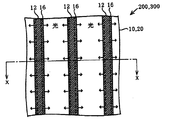
【解決手段】反射型LCD300の反射電極33の表面に対向して照明装置200が配置されている。照明装置200には、陽極11、ストライプ状の陰極12、及び有機層13からなる有機EL素子層15が形成されている。陰極12に対応した有機層13の領域が発光領域13aとなる。また、陰極12を覆って遮光層16が形成されている。さらに、反射型LCD300には、極力薄く形成可能な偏光板41として、アルミニウム層からなり複数の微細なスリットがパターニングにより形成された回折格子が配置されている。また、観察側の方から順に、第1の偏光板−第1の4分の1波長板−照明層−第2の4分の1波長板−第2の偏光板−反射型LCDの構成をとることもできる。
【選択図】図2
Description
照明層414の構成例を図6に示す。ガラスなどの透明絶縁材料からなる第1の透明基板520上には、ITOやIZO等の透明導電材料からなる第1の電極層(例えば陽極)522がその全面に形成されている。第1の電極層522の上には有機発光層を含む有機層524が全面に形成される。この有機層524の上には、アルミニムなどからなる第2の電極層(例えば陰極)526が格子状またはストライプ状にが形成され、その上に有機材料からなる接着剤層528を介し、ガラスなど第2の透明基板530が形成されている。
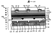
図9は、本実施形態に係るアクティブマトリクス型の反射型LCD420の第1の基板側の平面構成の一部、図10は、図9のA−A線に沿った位置における概略断面構成を示している。アクティブマトリクス型LCDでは、表示領域内にマトリクス状に複数の画素が設けられ、各画素に対してここでは、スイッチ素子としてTFT510が設けられている。
Claims (15)
- 照明装置と反射型液晶表示装置とを備えた表示装置であって、
前記照明装置は、透明基板と、この透明基板上に部分的に配置された発光薄体と、を備え、前記発光薄体の一方の面を前記反射型液晶表示装置の表示面に対向させて配置されており、
前記反射型液晶表示装置は、偏光板と、共通電極と、前記共通電極と対向して配置された反射電極と、前記共通電極上及び反射電極上のそれぞれに配置された1対の配向膜と、前記共通電極及び前記反射電極に挟まれた液晶層と、前記反射電極が配置された基板と、を備え、前記偏光板は、所定の金属層がパターニングされてなる回折格子であることを特徴とする表示装置。 - 前記所定の金属層は、アルミニウム層であることを特徴とする請求項1記載の表示装置。
- 照明装置と反射型液晶表示装置とを備えた表示装置であって、
前記照明装置は、透明基板と、この透明基板上に部分的に配置された発光薄体と、を備え、前記発光薄体の一方の面を前記反射型液晶表示装置の表示面に対向させて配置されており、
前記反射型液晶表示装置は、偏光板と、共通電極と、前記共通電極と対向して配置された反射電極と、前記共通電極上及び反射電極上のそれぞれに配置された1対の配向膜と、前記共通電極及び前記反射電極に挟まれた液晶層と、前記反射電極が配置された基板と、を備え、前記偏光板は、二色性染料分子を含む溶液の塗布及び固化により、その二色性染料分子が規則的に配列されてなることを特徴とする表示装置。 - 前記偏光板と前記共通電極との間に、光散乱層が配置されていることを特徴とする請求項1、2、3のうちいずれか1項に記載の表示装置。
- 前記発光薄体は、陽極及び陰極を備えた有機エレクトロルミネッセンス素子からなることを特徴とする請求項1、2、3、4のうちいずれか1項に記載の表示装置。
- 前記陽極又は陰極のうち少なくとも一方は、所定の形状にパターニングされていることを特徴とする請求項5記載の表示装置。
- 前記陰極が前記所定の形状にストライプ状にパターニングされ、その陰極が前記陽極の上方に配置されていることを特徴とする請求項6記載の表示装置。
- 前記有機エレクトロルミネッセンス素子は、前記陽極と陰極との間に電子輸送層、発光層、及び正孔輸送層を備え、前記電子輸送層、発光層及び正孔輸送層のうち、少なくとも一つが所定の形状にパターニングされていることを特徴とする請求項5記載の表示装置。
- 前記所定の形状はストライプ状であることを特徴とする請求項6、7、8のいずれか1項に記載の表示装置。
- 前記発光薄体の他方の面を覆うようにして、遮光層が配置されていることを特徴とする請求項1、2、3、4、5、6、7、8、9のいずれか1項に記載の表示装置。
- 観察側の表面に設けられ、その透過軸に沿った偏光を透過する第1の偏光板と、
前記第1の偏光板の下に設けられる第1の4分の1波長板と、
前記第1の4分の1波長板の下に設けられ、前記第1の4分の1波長板の下方の一部分において光を下方に向けて照射する照明層と、
前記照明層の下に設けられる第2の4分の1波長板と、
前記第2の4分の1波長板の下に設けられ、前記第1の偏光板と同一の方向の透過軸に沿った偏光を透過する第2の偏光板と、
液晶層に印加する電圧を制御することで、前記第2の偏光板からの偏光を液晶層の光学特性に基づいて変化させ、前記第2の偏光板から入射してくる光を反射射出する液晶表示部と、
を有することを特徴とする液晶表示装置。 - 請求項11に記載の液晶表示装置において、
前記第1の4分の1波長板は、前記第1の偏光板の透過軸と45°または135°ずれた遅相軸を有し、
前記第2の4分の1波長板は、前記第1の4分の1波長板の遅相軸に対し、90°または270°ずれた遅相軸を有することを特徴とする液晶表示装置。 - 請求項11に記載の液晶表示装置において、
前記照明層は、有機EL発光素子を含むことを特徴とする液晶表示装置。 - 請求項11、12、13のいずれか1項に記載の液晶表示装置において、
前記液晶表示部は、画素電極が画素毎に個別に形成されており、画素電極の電圧を個別に制御することで、画素毎に表示を制御することを特徴とする液晶表示装置。 - 請求項11、12、13、14のいずれか1項に記載の液晶表示装置において、
前記第1の偏光板の表面は、反射防止処理が施されていることを特徴とする液晶表示装置。
Priority Applications (1)
| Application Number | Priority Date | Filing Date | Title |
|---|---|---|---|
| JP2006141733A JP2007041536A (ja) | 2005-05-20 | 2006-05-22 | 表示装置及び液晶表示装置 |
Applications Claiming Priority (3)
| Application Number | Priority Date | Filing Date | Title |
|---|---|---|---|
| JP2005148544 | 2005-05-20 | ||
| JP2005195565 | 2005-07-04 | ||
| JP2006141733A JP2007041536A (ja) | 2005-05-20 | 2006-05-22 | 表示装置及び液晶表示装置 |
Publications (2)
| Publication Number | Publication Date |
|---|---|
| JP2007041536A true JP2007041536A (ja) | 2007-02-15 |
| JP2007041536A5 JP2007041536A5 (ja) | 2009-03-12 |
Family
ID=37799528
Family Applications (1)
| Application Number | Title | Priority Date | Filing Date |
|---|---|---|---|
| JP2006141733A Withdrawn JP2007041536A (ja) | 2005-05-20 | 2006-05-22 | 表示装置及び液晶表示装置 |
Country Status (1)
| Country | Link |
|---|---|
| JP (1) | JP2007041536A (ja) |
Cited By (14)
| Publication number | Priority date | Publication date | Assignee | Title |
|---|---|---|---|---|
| JP2009066205A (ja) * | 2007-09-13 | 2009-04-02 | Aruze Corp | 液晶ディスプレイ装置および液晶ディスプレイ装置を備えた遊技機 |
| JP2010050083A (ja) * | 2008-08-19 | 2010-03-04 | Samsung Mobile Display Co Ltd | 有機発光表示装置 |
| CN101881887A (zh) * | 2009-05-08 | 2010-11-10 | 日东电工株式会社 | 视频观看设备和自发光型显示器 |
| JP2012014904A (ja) * | 2010-06-30 | 2012-01-19 | Seiko Epson Corp | 照明装置、及び電気光学装置 |
| US8148894B2 (en) | 2008-08-27 | 2012-04-03 | Samsung Mobile Display Co., Ltd. | Organic light emitting diode display |
| US8169386B2 (en) | 2008-08-19 | 2012-05-01 | Samsung Mobile Display Co., Ltd. | Organic light emitting diode display |
| US8198802B2 (en) | 2008-07-25 | 2012-06-12 | Samsung Mobile Display Co., Ltd. | Organic light emitting diode display for suppressing reflection of external light |
| US8220943B2 (en) | 2009-03-05 | 2012-07-17 | Seiko Epson Corporation | Illumination device and display apparatus |
| JP2013120319A (ja) * | 2011-12-08 | 2013-06-17 | Sharp Corp | 液晶表示装置 |
| CN106992202A (zh) * | 2017-04-10 | 2017-07-28 | 京东方科技集团股份有限公司 | 光源面板和显示装置 |
| JP2018066960A (ja) * | 2016-10-21 | 2018-04-26 | 株式会社半導体エネルギー研究所 | 表示装置の作製方法 |
| JP2018066944A (ja) * | 2016-10-21 | 2018-04-26 | 株式会社半導体エネルギー研究所 | 表示装置の作製方法 |
| CN114384723A (zh) * | 2020-10-20 | 2022-04-22 | 京东方科技集团股份有限公司 | 一种前置光源及其制作方法、显示装置 |
| WO2023184342A1 (zh) * | 2022-03-31 | 2023-10-05 | 京东方科技集团股份有限公司 | 发光基板及其制备方法、显示装置 |
Citations (7)
| Publication number | Priority date | Publication date | Assignee | Title |
|---|---|---|---|---|
| JPH09133913A (ja) * | 1995-11-08 | 1997-05-20 | Hitachi Ltd | 反射型カラー液晶表示装置 |
| JPH1073722A (ja) * | 1996-08-30 | 1998-03-17 | Sony Corp | 偏光光学素子及びその製造方法 |
| JP2000267091A (ja) * | 1999-03-17 | 2000-09-29 | Hitachi Ltd | 液晶表示装置 |
| JP2002216961A (ja) * | 2001-01-19 | 2002-08-02 | Seiko Epson Corp | 照明装置と液晶表示装置および電子機器と照明装置の製造方法 |
| JP2003005170A (ja) * | 2001-04-16 | 2003-01-08 | Seiko Epson Corp | 液晶装置及び投射型表示装置 |
| JP2003233072A (ja) * | 2002-02-12 | 2003-08-22 | Seiko Epson Corp | 電気光学装置、その製造方法、照明装置、及び電子機器 |
| JP2003330021A (ja) * | 2002-03-06 | 2003-11-19 | Seiko Epson Corp | 電気光学装置、および電子機器 |
-
2006
- 2006-05-22 JP JP2006141733A patent/JP2007041536A/ja not_active Withdrawn
Patent Citations (7)
| Publication number | Priority date | Publication date | Assignee | Title |
|---|---|---|---|---|
| JPH09133913A (ja) * | 1995-11-08 | 1997-05-20 | Hitachi Ltd | 反射型カラー液晶表示装置 |
| JPH1073722A (ja) * | 1996-08-30 | 1998-03-17 | Sony Corp | 偏光光学素子及びその製造方法 |
| JP2000267091A (ja) * | 1999-03-17 | 2000-09-29 | Hitachi Ltd | 液晶表示装置 |
| JP2002216961A (ja) * | 2001-01-19 | 2002-08-02 | Seiko Epson Corp | 照明装置と液晶表示装置および電子機器と照明装置の製造方法 |
| JP2003005170A (ja) * | 2001-04-16 | 2003-01-08 | Seiko Epson Corp | 液晶装置及び投射型表示装置 |
| JP2003233072A (ja) * | 2002-02-12 | 2003-08-22 | Seiko Epson Corp | 電気光学装置、その製造方法、照明装置、及び電子機器 |
| JP2003330021A (ja) * | 2002-03-06 | 2003-11-19 | Seiko Epson Corp | 電気光学装置、および電子機器 |
Cited By (16)
| Publication number | Priority date | Publication date | Assignee | Title |
|---|---|---|---|---|
| JP2009066205A (ja) * | 2007-09-13 | 2009-04-02 | Aruze Corp | 液晶ディスプレイ装置および液晶ディスプレイ装置を備えた遊技機 |
| US8198802B2 (en) | 2008-07-25 | 2012-06-12 | Samsung Mobile Display Co., Ltd. | Organic light emitting diode display for suppressing reflection of external light |
| JP2010050083A (ja) * | 2008-08-19 | 2010-03-04 | Samsung Mobile Display Co Ltd | 有機発光表示装置 |
| US8169386B2 (en) | 2008-08-19 | 2012-05-01 | Samsung Mobile Display Co., Ltd. | Organic light emitting diode display |
| US8148894B2 (en) | 2008-08-27 | 2012-04-03 | Samsung Mobile Display Co., Ltd. | Organic light emitting diode display |
| US8684549B2 (en) | 2009-03-05 | 2014-04-01 | Seiko Epson Corporation | Illumination device and display apparatus |
| US8220943B2 (en) | 2009-03-05 | 2012-07-17 | Seiko Epson Corporation | Illumination device and display apparatus |
| CN101881887A (zh) * | 2009-05-08 | 2010-11-10 | 日东电工株式会社 | 视频观看设备和自发光型显示器 |
| JP2012014904A (ja) * | 2010-06-30 | 2012-01-19 | Seiko Epson Corp | 照明装置、及び電気光学装置 |
| JP2013120319A (ja) * | 2011-12-08 | 2013-06-17 | Sharp Corp | 液晶表示装置 |
| JP2018066960A (ja) * | 2016-10-21 | 2018-04-26 | 株式会社半導体エネルギー研究所 | 表示装置の作製方法 |
| JP2018066944A (ja) * | 2016-10-21 | 2018-04-26 | 株式会社半導体エネルギー研究所 | 表示装置の作製方法 |
| CN106992202A (zh) * | 2017-04-10 | 2017-07-28 | 京东方科技集团股份有限公司 | 光源面板和显示装置 |
| US11271051B2 (en) | 2017-04-10 | 2022-03-08 | Boe Technology Group Co., Ltd. | Light source panel and display device |
| CN114384723A (zh) * | 2020-10-20 | 2022-04-22 | 京东方科技集团股份有限公司 | 一种前置光源及其制作方法、显示装置 |
| WO2023184342A1 (zh) * | 2022-03-31 | 2023-10-05 | 京东方科技集团股份有限公司 | 发光基板及其制备方法、显示装置 |
Similar Documents
| Publication | Publication Date | Title |
|---|---|---|
| JP2007041536A (ja) | 表示装置及び液晶表示装置 | |
| KR100800931B1 (ko) | 표시 장치 | |
| KR100800932B1 (ko) | 표시 장치 | |
| JP3898012B2 (ja) | 表示装置 | |
| US9436053B2 (en) | Display unit and electronic apparatus | |
| KR100621495B1 (ko) | 화상 표시 상태와 거울 상태를 전환 가능한 장치, 및이것을 구비한 기기 | |
| JP3993221B2 (ja) | 表示装置 | |
| JP2006323302A (ja) | 表示装置 | |
| JP2006164808A (ja) | 発光素子,照明装置及びこれを有する表示装置 | |
| JP3767255B2 (ja) | 液晶装置及び電子機器 | |
| JP2006323303A (ja) | 表示装置 | |
| KR20090079779A (ko) | 듀얼 액정표시장치 | |
| JP2010250025A (ja) | 偏光素子とその製造方法および液晶表示装置 | |
| JP4211344B2 (ja) | 表示装置及びこれを備えた電子機器 | |
| CN105445997B (zh) | 液晶显示装置 | |
| JP2004212945A (ja) | 反射型液晶表示装置 | |
| JP2006234963A (ja) | 液晶表示装置 | |
| US8570463B2 (en) | Liquid crystal display device | |
| JP4826997B2 (ja) | 表示装置 | |
| JP2005534989A (ja) | 反射透過型液晶表示装置 | |
| US20180329255A1 (en) | Color filter substrate and liquid crystal display | |
| JP5624014B2 (ja) | 液晶表示装置 | |
| KR102456429B1 (ko) | 디스플레이 장치 | |
| JP2005309377A (ja) | 液晶表示装置 | |
| KR20110031010A (ko) | 반사투과형 액정표시소자 |
Legal Events
| Date | Code | Title | Description |
|---|---|---|---|
| RD04 | Notification of resignation of power of attorney |
Free format text: JAPANESE INTERMEDIATE CODE: A7424 Effective date: 20071220 |
|
| RD03 | Notification of appointment of power of attorney |
Free format text: JAPANESE INTERMEDIATE CODE: A7423 Effective date: 20071226 |
|
| A521 | Request for written amendment filed |
Free format text: JAPANESE INTERMEDIATE CODE: A523 Effective date: 20090126 |
|
| A621 | Written request for application examination |
Free format text: JAPANESE INTERMEDIATE CODE: A621 Effective date: 20090126 |
|
| A977 | Report on retrieval |
Free format text: JAPANESE INTERMEDIATE CODE: A971007 Effective date: 20110817 |
|
| A131 | Notification of reasons for refusal |
Free format text: JAPANESE INTERMEDIATE CODE: A131 Effective date: 20110920 |
|
| A761 | Written withdrawal of application |
Free format text: JAPANESE INTERMEDIATE CODE: A761 Effective date: 20111012 |