JP2006519931A - Method of electroplating processed products having high aspect ratio holes - Google Patents
Method of electroplating processed products having high aspect ratio holes Download PDFInfo
- Publication number
- JP2006519931A JP2006519931A JP2006504539A JP2006504539A JP2006519931A JP 2006519931 A JP2006519931 A JP 2006519931A JP 2006504539 A JP2006504539 A JP 2006504539A JP 2006504539 A JP2006504539 A JP 2006504539A JP 2006519931 A JP2006519931 A JP 2006519931A
- Authority
- JP
- Japan
- Prior art keywords
- workpiece
- pulse
- current pulse
- current
- reverse current
- Prior art date
- Legal status (The legal status is an assumption and is not a legal conclusion. Google has not performed a legal analysis and makes no representation as to the accuracy of the status listed.)
- Ceased
Links
- 238000000034 method Methods 0.000 title claims abstract description 40
- 238000009713 electroplating Methods 0.000 title claims description 14
- 238000007747 plating Methods 0.000 claims abstract description 66
- 230000002441 reversible effect Effects 0.000 claims abstract description 66
- 239000003792 electrolyte Substances 0.000 claims abstract description 54
- 229910052751 metal Inorganic materials 0.000 claims abstract description 31
- 239000002184 metal Substances 0.000 claims abstract description 31
- RYGMFSIKBFXOCR-UHFFFAOYSA-N Copper Chemical compound [Cu] RYGMFSIKBFXOCR-UHFFFAOYSA-N 0.000 claims description 35
- 229910052802 copper Inorganic materials 0.000 claims description 32
- 239000010949 copper Substances 0.000 claims description 32
- JPVYNHNXODAKFH-UHFFFAOYSA-N Cu2+ Chemical compound [Cu+2] JPVYNHNXODAKFH-UHFFFAOYSA-N 0.000 claims description 11
- 229910001431 copper ion Inorganic materials 0.000 claims description 11
- 150000001875 compounds Chemical class 0.000 claims description 8
- 230000001590 oxidative effect Effects 0.000 claims description 4
- 150000002506 iron compounds Chemical class 0.000 claims description 3
- 238000003756 stirring Methods 0.000 claims description 2
- 238000012360 testing method Methods 0.000 description 30
- 238000013019 agitation Methods 0.000 description 14
- 239000007921 spray Substances 0.000 description 12
- 239000000243 solution Substances 0.000 description 11
- 238000000151 deposition Methods 0.000 description 10
- 230000008021 deposition Effects 0.000 description 10
- 238000002474 experimental method Methods 0.000 description 10
- 239000012530 fluid Substances 0.000 description 10
- BASFCYQUMIYNBI-UHFFFAOYSA-N platinum Chemical compound [Pt] BASFCYQUMIYNBI-UHFFFAOYSA-N 0.000 description 8
- -1 trivalent iron ions Chemical class 0.000 description 8
- 238000004070 electrodeposition Methods 0.000 description 6
- 238000004519 manufacturing process Methods 0.000 description 6
- 229910000510 noble metal Inorganic materials 0.000 description 6
- 239000000758 substrate Substances 0.000 description 6
- 230000006872 improvement Effects 0.000 description 5
- 238000009434 installation Methods 0.000 description 5
- 229910052760 oxygen Inorganic materials 0.000 description 5
- 239000001301 oxygen Substances 0.000 description 5
- CWYNVVGOOAEACU-UHFFFAOYSA-N Fe2+ Chemical compound [Fe+2] CWYNVVGOOAEACU-UHFFFAOYSA-N 0.000 description 4
- RTAQQCXQSZGOHL-UHFFFAOYSA-N Titanium Chemical compound [Ti] RTAQQCXQSZGOHL-UHFFFAOYSA-N 0.000 description 4
- 229910052697 platinum Inorganic materials 0.000 description 4
- 230000008569 process Effects 0.000 description 4
- 229910052719 titanium Inorganic materials 0.000 description 4
- 239000010936 titanium Substances 0.000 description 4
- VTLYFUHAOXGGBS-UHFFFAOYSA-N Fe3+ Chemical compound [Fe+3] VTLYFUHAOXGGBS-UHFFFAOYSA-N 0.000 description 3
- QAOWNCQODCNURD-UHFFFAOYSA-N Sulfuric acid Chemical compound OS(O)(=O)=O QAOWNCQODCNURD-UHFFFAOYSA-N 0.000 description 3
- QVGXLLKOCUKJST-UHFFFAOYSA-N atomic oxygen Chemical compound [O] QVGXLLKOCUKJST-UHFFFAOYSA-N 0.000 description 3
- 230000008901 benefit Effects 0.000 description 3
- 238000009826 distribution Methods 0.000 description 3
- 238000005868 electrolysis reaction Methods 0.000 description 3
- 150000002500 ions Chemical class 0.000 description 3
- XEEYBQQBJWHFJM-UHFFFAOYSA-N iron Substances [Fe] XEEYBQQBJWHFJM-UHFFFAOYSA-N 0.000 description 3
- BAUYGSIQEAFULO-UHFFFAOYSA-L iron(2+) sulfate (anhydrous) Chemical compound [Fe+2].[O-]S([O-])(=O)=O BAUYGSIQEAFULO-UHFFFAOYSA-L 0.000 description 3
- 150000004706 metal oxides Chemical class 0.000 description 3
- 239000000203 mixture Substances 0.000 description 3
- 238000000917 particle-image velocimetry Methods 0.000 description 3
- 238000012545 processing Methods 0.000 description 3
- OKTJSMMVPCPJKN-UHFFFAOYSA-N Carbon Chemical compound [C] OKTJSMMVPCPJKN-UHFFFAOYSA-N 0.000 description 2
- VEXZGXHMUGYJMC-UHFFFAOYSA-M Chloride anion Chemical compound [Cl-] VEXZGXHMUGYJMC-UHFFFAOYSA-M 0.000 description 2
- KDLHZDBZIXYQEI-UHFFFAOYSA-N Palladium Chemical compound [Pd] KDLHZDBZIXYQEI-UHFFFAOYSA-N 0.000 description 2
- KJTLSVCANCCWHF-UHFFFAOYSA-N Ruthenium Chemical compound [Ru] KJTLSVCANCCWHF-UHFFFAOYSA-N 0.000 description 2
- 239000000969 carrier Substances 0.000 description 2
- OZECDDHOAMNMQI-UHFFFAOYSA-H cerium(3+);trisulfate Chemical compound [Ce+3].[Ce+3].[O-]S([O-])(=O)=O.[O-]S([O-])(=O)=O.[O-]S([O-])(=O)=O OZECDDHOAMNMQI-UHFFFAOYSA-H 0.000 description 2
- 239000011248 coating agent Substances 0.000 description 2
- 230000000694 effects Effects 0.000 description 2
- 239000008151 electrolyte solution Substances 0.000 description 2
- PCHJSUWPFVWCPO-UHFFFAOYSA-N gold Chemical compound [Au] PCHJSUWPFVWCPO-UHFFFAOYSA-N 0.000 description 2
- 229910052737 gold Inorganic materials 0.000 description 2
- 239000010931 gold Substances 0.000 description 2
- 229910052741 iridium Inorganic materials 0.000 description 2
- GKOZUEZYRPOHIO-UHFFFAOYSA-N iridium atom Chemical compound [Ir] GKOZUEZYRPOHIO-UHFFFAOYSA-N 0.000 description 2
- 229910052742 iron Inorganic materials 0.000 description 2
- 229910000359 iron(II) sulfate Inorganic materials 0.000 description 2
- 239000007788 liquid Substances 0.000 description 2
- 238000001465 metallisation Methods 0.000 description 2
- 238000012986 modification Methods 0.000 description 2
- 230000004048 modification Effects 0.000 description 2
- 239000002245 particle Substances 0.000 description 2
- 230000000737 periodic effect Effects 0.000 description 2
- 230000010363 phase shift Effects 0.000 description 2
- 238000005086 pumping Methods 0.000 description 2
- 238000011160 research Methods 0.000 description 2
- 229910052703 rhodium Inorganic materials 0.000 description 2
- 239000010948 rhodium Substances 0.000 description 2
- MHOVAHRLVXNVSD-UHFFFAOYSA-N rhodium atom Chemical compound [Rh] MHOVAHRLVXNVSD-UHFFFAOYSA-N 0.000 description 2
- 229910052707 ruthenium Inorganic materials 0.000 description 2
- PXLIDIMHPNPGMH-UHFFFAOYSA-N sodium chromate Chemical compound [Na+].[Na+].[O-][Cr]([O-])(=O)=O PXLIDIMHPNPGMH-UHFFFAOYSA-N 0.000 description 2
- 238000012546 transfer Methods 0.000 description 2
- 238000011144 upstream manufacturing Methods 0.000 description 2
- 229910052684 Cerium Inorganic materials 0.000 description 1
- VYZAMTAEIAYCRO-UHFFFAOYSA-N Chromium Chemical compound [Cr] VYZAMTAEIAYCRO-UHFFFAOYSA-N 0.000 description 1
- PWHULOQIROXLJO-UHFFFAOYSA-N Manganese Chemical compound [Mn] PWHULOQIROXLJO-UHFFFAOYSA-N 0.000 description 1
- 229910002651 NO3 Inorganic materials 0.000 description 1
- NHNBFGGVMKEFGY-UHFFFAOYSA-N Nitrate Chemical compound [O-][N+]([O-])=O NHNBFGGVMKEFGY-UHFFFAOYSA-N 0.000 description 1
- BQCADISMDOOEFD-UHFFFAOYSA-N Silver Chemical compound [Ag] BQCADISMDOOEFD-UHFFFAOYSA-N 0.000 description 1
- 239000002253 acid Substances 0.000 description 1
- 230000002378 acidificating effect Effects 0.000 description 1
- 239000000654 additive Substances 0.000 description 1
- 230000000996 additive effect Effects 0.000 description 1
- 229910045601 alloy Inorganic materials 0.000 description 1
- 239000000956 alloy Substances 0.000 description 1
- 150000001450 anions Chemical class 0.000 description 1
- 239000007864 aqueous solution Substances 0.000 description 1
- 230000015572 biosynthetic process Effects 0.000 description 1
- 229910052799 carbon Inorganic materials 0.000 description 1
- ZMIGMASIKSOYAM-UHFFFAOYSA-N cerium Chemical compound [Ce][Ce][Ce][Ce][Ce][Ce][Ce][Ce][Ce][Ce][Ce][Ce][Ce][Ce][Ce][Ce][Ce][Ce][Ce][Ce][Ce][Ce][Ce][Ce][Ce][Ce][Ce][Ce][Ce][Ce][Ce][Ce][Ce][Ce][Ce][Ce][Ce][Ce] ZMIGMASIKSOYAM-UHFFFAOYSA-N 0.000 description 1
- VZDYWEUILIUIDF-UHFFFAOYSA-J cerium(4+);disulfate Chemical compound [Ce+4].[O-]S([O-])(=O)=O.[O-]S([O-])(=O)=O VZDYWEUILIUIDF-UHFFFAOYSA-J 0.000 description 1
- 230000008859 change Effects 0.000 description 1
- 229910052804 chromium Inorganic materials 0.000 description 1
- 239000011651 chromium Substances 0.000 description 1
- 239000004020 conductor Substances 0.000 description 1
- 238000005260 corrosion Methods 0.000 description 1
- 230000007797 corrosion Effects 0.000 description 1
- 238000000354 decomposition reaction Methods 0.000 description 1
- 230000003247 decreasing effect Effects 0.000 description 1
- 230000001419 dependent effect Effects 0.000 description 1
- 238000009792 diffusion process Methods 0.000 description 1
- HTXDPTMKBJXEOW-UHFFFAOYSA-N dioxoiridium Chemical compound O=[Ir]=O HTXDPTMKBJXEOW-UHFFFAOYSA-N 0.000 description 1
- 230000005518 electrochemistry Effects 0.000 description 1
- 238000005516 engineering process Methods 0.000 description 1
- 239000007789 gas Substances 0.000 description 1
- 229910002804 graphite Inorganic materials 0.000 description 1
- 239000010439 graphite Substances 0.000 description 1
- 230000009931 harmful effect Effects 0.000 description 1
- 238000002347 injection Methods 0.000 description 1
- 239000007924 injection Substances 0.000 description 1
- 229910000457 iridium oxide Inorganic materials 0.000 description 1
- 229910000358 iron sulfate Inorganic materials 0.000 description 1
- SURQXAFEQWPFPV-UHFFFAOYSA-L iron(2+) sulfate heptahydrate Chemical compound O.O.O.O.O.O.O.[Fe+2].[O-]S([O-])(=O)=O SURQXAFEQWPFPV-UHFFFAOYSA-L 0.000 description 1
- 230000001788 irregular Effects 0.000 description 1
- 229910052748 manganese Inorganic materials 0.000 description 1
- 239000011572 manganese Substances 0.000 description 1
- 229940099596 manganese sulfate Drugs 0.000 description 1
- 235000007079 manganese sulphate Nutrition 0.000 description 1
- 239000011702 manganese sulphate Substances 0.000 description 1
- PAVJEQIFHXNOSM-UHFFFAOYSA-H manganese(3+);trisulfate Chemical compound [Mn+3].[Mn+3].[O-]S([O-])(=O)=O.[O-]S([O-])(=O)=O.[O-]S([O-])(=O)=O PAVJEQIFHXNOSM-UHFFFAOYSA-H 0.000 description 1
- SQQMAOCOWKFBNP-UHFFFAOYSA-L manganese(II) sulfate Chemical compound [Mn+2].[O-]S([O-])(=O)=O SQQMAOCOWKFBNP-UHFFFAOYSA-L 0.000 description 1
- 239000000463 material Substances 0.000 description 1
- 238000005259 measurement Methods 0.000 description 1
- 230000007246 mechanism Effects 0.000 description 1
- 229910021645 metal ion Inorganic materials 0.000 description 1
- 229910044991 metal oxide Inorganic materials 0.000 description 1
- 150000002739 metals Chemical class 0.000 description 1
- 239000011859 microparticle Substances 0.000 description 1
- 238000002156 mixing Methods 0.000 description 1
- 239000006259 organic additive Substances 0.000 description 1
- 229910052762 osmium Inorganic materials 0.000 description 1
- SYQBFIAQOQZEGI-UHFFFAOYSA-N osmium atom Chemical compound [Os] SYQBFIAQOQZEGI-UHFFFAOYSA-N 0.000 description 1
- 150000002926 oxygen Chemical class 0.000 description 1
- 229910052763 palladium Inorganic materials 0.000 description 1
- 230000010287 polarization Effects 0.000 description 1
- 239000011148 porous material Substances 0.000 description 1
- 230000002787 reinforcement Effects 0.000 description 1
- 230000003014 reinforcing effect Effects 0.000 description 1
- 238000010517 secondary reaction Methods 0.000 description 1
- 239000004065 semiconductor Substances 0.000 description 1
- 229910052709 silver Inorganic materials 0.000 description 1
- 239000004332 silver Substances 0.000 description 1
- CMZUMMUJMWNLFH-UHFFFAOYSA-N sodium metavanadate Chemical compound [Na+].[O-][V](=O)=O CMZUMMUJMWNLFH-UHFFFAOYSA-N 0.000 description 1
- 238000005507 spraying Methods 0.000 description 1
- 238000004544 sputter deposition Methods 0.000 description 1
- 235000011149 sulphuric acid Nutrition 0.000 description 1
- 239000001117 sulphuric acid Substances 0.000 description 1
- 230000003746 surface roughness Effects 0.000 description 1
- 229910052715 tantalum Inorganic materials 0.000 description 1
- GUVRBAGPIYLISA-UHFFFAOYSA-N tantalum atom Chemical compound [Ta] GUVRBAGPIYLISA-UHFFFAOYSA-N 0.000 description 1
- 229910052720 vanadium Inorganic materials 0.000 description 1
- GPPXJZIENCGNKB-UHFFFAOYSA-N vanadium Chemical compound [V]#[V] GPPXJZIENCGNKB-UHFFFAOYSA-N 0.000 description 1
- 235000012431 wafers Nutrition 0.000 description 1
Images


Classifications
-
- C—CHEMISTRY; METALLURGY
- C25—ELECTROLYTIC OR ELECTROPHORETIC PROCESSES; APPARATUS THEREFOR
- C25D—PROCESSES FOR THE ELECTROLYTIC OR ELECTROPHORETIC PRODUCTION OF COATINGS; ELECTROFORMING; APPARATUS THEREFOR
- C25D5/00—Electroplating characterised by the process; Pretreatment or after-treatment of workpieces
- C25D5/18—Electroplating using modulated, pulsed or reversing current
-
- C—CHEMISTRY; METALLURGY
- C25—ELECTROLYTIC OR ELECTROPHORETIC PROCESSES; APPARATUS THEREFOR
- C25D—PROCESSES FOR THE ELECTROLYTIC OR ELECTROPHORETIC PRODUCTION OF COATINGS; ELECTROFORMING; APPARATUS THEREFOR
- C25D5/00—Electroplating characterised by the process; Pretreatment or after-treatment of workpieces
- C25D5/08—Electroplating with moving electrolyte e.g. jet electroplating
-
- C—CHEMISTRY; METALLURGY
- C25—ELECTROLYTIC OR ELECTROPHORETIC PROCESSES; APPARATUS THEREFOR
- C25D—PROCESSES FOR THE ELECTROLYTIC OR ELECTROPHORETIC PRODUCTION OF COATINGS; ELECTROFORMING; APPARATUS THEREFOR
- C25D7/00—Electroplating characterised by the article coated
- C25D7/12—Semiconductors
-
- H—ELECTRICITY
- H05—ELECTRIC TECHNIQUES NOT OTHERWISE PROVIDED FOR
- H05K—PRINTED CIRCUITS; CASINGS OR CONSTRUCTIONAL DETAILS OF ELECTRIC APPARATUS; MANUFACTURE OF ASSEMBLAGES OF ELECTRICAL COMPONENTS
- H05K3/00—Apparatus or processes for manufacturing printed circuits
- H05K3/40—Forming printed elements for providing electric connections to or between printed circuits
- H05K3/42—Plated through-holes or plated via connections
- H05K3/423—Plated through-holes or plated via connections characterised by electroplating method
-
- H—ELECTRICITY
- H01—ELECTRIC ELEMENTS
- H01L—SEMICONDUCTOR DEVICES NOT COVERED BY CLASS H10
- H01L21/00—Processes or apparatus adapted for the manufacture or treatment of semiconductor or solid state devices or of parts thereof
- H01L21/02—Manufacture or treatment of semiconductor devices or of parts thereof
- H01L21/04—Manufacture or treatment of semiconductor devices or of parts thereof the devices having potential barriers, e.g. a PN junction, depletion layer or carrier concentration layer
- H01L21/18—Manufacture or treatment of semiconductor devices or of parts thereof the devices having potential barriers, e.g. a PN junction, depletion layer or carrier concentration layer the devices having semiconductor bodies comprising elements of Group IV of the Periodic Table or AIIIBV compounds with or without impurities, e.g. doping materials
- H01L21/28—Manufacture of electrodes on semiconductor bodies using processes or apparatus not provided for in groups H01L21/20 - H01L21/268
- H01L21/283—Deposition of conductive or insulating materials for electrodes conducting electric current
- H01L21/288—Deposition of conductive or insulating materials for electrodes conducting electric current from a liquid, e.g. electrolytic deposition
- H01L21/2885—Deposition of conductive or insulating materials for electrodes conducting electric current from a liquid, e.g. electrolytic deposition using an external electrical current, i.e. electro-deposition
-
- H—ELECTRICITY
- H05—ELECTRIC TECHNIQUES NOT OTHERWISE PROVIDED FOR
- H05K—PRINTED CIRCUITS; CASINGS OR CONSTRUCTIONAL DETAILS OF ELECTRIC APPARATUS; MANUFACTURE OF ASSEMBLAGES OF ELECTRICAL COMPONENTS
- H05K2203/00—Indexing scheme relating to apparatus or processes for manufacturing printed circuits covered by H05K3/00
- H05K2203/14—Related to the order of processing steps
- H05K2203/1492—Periodical treatments, e.g. pulse plating of through-holes
-
- H—ELECTRICITY
- H05—ELECTRIC TECHNIQUES NOT OTHERWISE PROVIDED FOR
- H05K—PRINTED CIRCUITS; CASINGS OR CONSTRUCTIONAL DETAILS OF ELECTRIC APPARATUS; MANUFACTURE OF ASSEMBLAGES OF ELECTRICAL COMPONENTS
- H05K2203/00—Indexing scheme relating to apparatus or processes for manufacturing printed circuits covered by H05K3/00
- H05K2203/15—Position of the PCB during processing
- H05K2203/1572—Processing both sides of a PCB by the same process; Providing a similar arrangement of components on both sides; Making interlayer connections from two sides
Landscapes
- Chemical & Material Sciences (AREA)
- Engineering & Computer Science (AREA)
- Chemical Kinetics & Catalysis (AREA)
- Electrochemistry (AREA)
- Materials Engineering (AREA)
- Metallurgy (AREA)
- Organic Chemistry (AREA)
- Manufacturing & Machinery (AREA)
- Microelectronics & Electronic Packaging (AREA)
- Electroplating Methods And Accessories (AREA)
- Electroplating And Plating Baths Therefor (AREA)
Abstract
高アスペクト比のホールを備えて成る加工品を電気めっきするために、加工品及び少なくとも一つの陽極と金属めっき電解液とが接触する工程と、加工品と陽極間に電圧を印加することで、その結果、電流の流れが加工品に生じる工程とを備えて成る方法を明らかにする。電流の流れは、多くとも約6Hzの周波数を有するパルス逆電流の流れである。周波数に従って、それぞれの周期時間は少なくとも一つの順電流パルスと少なくとも一つの逆電流パルスを備えて成る。In order to electroplate a workpiece comprising a high aspect ratio hole, the step of contacting the workpiece and at least one anode with a metal plating electrolyte, and applying a voltage between the workpiece and the anode, As a result, a method comprising the step of generating a current flow in a workpiece is clarified. The current flow is a pulsed reverse current flow having a frequency of at most about 6 Hz. Depending on the frequency, each cycle time comprises at least one forward current pulse and at least one reverse current pulse.
Description
高アスペクト比のプリント回路基板、例えば、いわゆるバックパネルの製造は、良質の電解銅の金属被覆法にとって、よく知られた問題点を有している。パネルは、概してアスペクト比10:1で3mmから10mmまでの厚みである。しかしながら、なお一層厚いパネルが求められ、しかも15:1までのアスペクト比を備えることが、最近の傾向である。自らの重量のために取り扱いにおいて更なる問題点を与える「通常の」製造パネルよりも、そのようなパネルは概して大きくすることができる。銅析出・蒸着における制限要因の一つは、高アスペクト比のホールへのイオンの物質移動である。パターンプレートでレジストにオーバーめっきを引き起こす表面オーバーめっきなしに、あるいはパネルプレートでライン画定を乏しくせずにホールにおいて所望の銅厚さを達成することが、高アスペクト比のパネル製造における主要な問題点である。バックパネルでの別要因は、銅の蒸着分布がうまくいかない時に、圧入技術を用いる部品実装の難しさである。均一電着性問題を克服するために、明らかに生産性に否定的な影響を与える低い電気めっき電流密度が用いられてきた。これらの問題の解決法として、特許文献1や特許文献2に記述されるように、逆パルスめっきは、より高い電流密度の使用を許容可能として、スルーホール中の表面分布及び均一電着性を向上させる。
The manufacture of high aspect ratio printed circuit boards, such as so-called back panels, has a well-known problem for good quality electrolytic copper metallization. Panels are generally 3 mm to 10 mm thick with an aspect ratio of 10: 1. However, there is a recent trend to require even thicker panels and to have aspect ratios up to 15: 1. Such panels can generally be made larger than “normal” production panels, which present additional problems in handling due to their weight. One of the limiting factors in copper deposition / deposition is the mass transfer of ions into high aspect ratio holes. Achieving the desired copper thickness in holes without surface overplating that causes resist overplating in the pattern plate or without poor line definition in the panel plate is a major problem in high aspect ratio panel manufacturing. It is. Another factor in the back panel is the difficulty of component mounting using press-fit technology when the copper deposition distribution is not good. In order to overcome the throwing power problem, low electroplating current densities have been used that clearly have a negative impact on productivity. As a solution to these problems, as described in
プリント回路基板の水平処理において、Uniplate(登録商標:Atotech Deutschland GmbH)システムにおける高アスペクト比の均一電着性が、より厚いパネルの製造には、その使用を制限することが明らかになった。1.6mmよりも厚いパネルでさえ、銅の均一電着性はアスペクト比しだいでは十分に満足できるものではなかった。この理由は、ブラインドマイクロビアでのより高い電流密度で、より薄い材料の製造を重要視したためである。平均10A/dm2程度の高電流密度及びそのような条件下でブラインドマイクロビアを生成することは、35g/リットル以上の比較的高い銅濃度の使用を必要とした。これら双方の要因が、高アスペクト比のパネルに最良の均一電着性を不可能にしていた。標準的なInpulse(登録商標:Atotech Deutschland GmbH)装置で、均一電着性を改良するために実験が行われた。しかし、これらは、わずかな改善しか与えられなかった。これらの実験では、標準のInpulse(登録商標)システム(不活性アノードを有した銅メッキシステム、鉄(II)/鉄(III)の酸化還元システムと垂直及び水平メッキ装置における逆パルス電流技術を用いる)で使用可能なパルスパラメーターによって限定された。 In horizontal processing of printed circuit boards, high aspect ratio electrodeposition in the Uniplate (Atotech Deutschland GmbH) system has been found to limit its use for the production of thicker panels. Even with panels thicker than 1.6 mm, the throwing power of copper was not fully satisfactory depending on the aspect ratio. This is due to the importance of manufacturing thinner materials at higher current densities in blind microvias. Generating blind microvias under such conditions with high current densities on the order of 10 A / dm 2 required the use of relatively high copper concentrations of 35 g / liter or higher. Both of these factors made it impossible to achieve the best throwing power for high aspect ratio panels. Experiments were conducted to improve throwing power on a standard Inpulse (Atotech Deutschland GmbH) apparatus. However, these gave only a slight improvement. These experiments use the standard Inpulse® system (copper plating system with inert anode, iron (II) / iron (III) redox system and reverse pulse current technique in vertical and horizontal plating equipment) ) Was limited by the available pulse parameters.
Kruseは、非特許文献1で、例えばプリント回路基板の逆パルスめっき法を記述しており、その方法では、オフパルスによって断続・間欠する二つの順パルスの合計持続時間が5〜250msに設定され、逆パルスの持続時間が0〜5msに設定される。
Kruse describes, for example, a reverse pulse plating method for a printed circuit board in Non-Patent
特許文献3では、サブストレート(基板)上に金属をパルス電気めっきする方法が記述され、電着(陰極の)パルスが約500〜3000msの範囲にわたり、一方で、電気溶解(陽極の)パルスが約1〜300msにわたる。 In US Pat. No. 6,057,034, a method of pulse electroplating a metal on a substrate (substrate) is described, wherein an electrodeposition (cathode) pulse ranges from about 500 to 3000 ms, while an electrodissolution (anode) pulse is present. It takes about 1 to 300 ms.
プリント回路基板の逆パルスめっきにおいて、順パルスの持続時間は、しばしば10〜80msに設定され、逆パルスの持続時間は、0.5〜6msに設定される。これは、約12から約95Hzの周波数範囲となる。仮に、2mm厚でアスペクト比10:1のスルーホールを含んだプリント回路基板が製造されるとすると、スルーホール中の銅蒸着の許容可能な均一電着性は、順パルスでは1〜10A/dm2の範囲の電流密度で、逆パルスでは10〜40A/dm2の範囲の電流密度で実現された。仮に2mmよりも大きな厚さのプリント回路基板が製造されるとすると、電流密度は、許容しうる均一電着性を達成するために減らされなければならない。 In reverse pulse plating of printed circuit boards, the forward pulse duration is often set to 10-80 ms and the reverse pulse duration is set to 0.5-6 ms. This results in a frequency range of about 12 to about 95 Hz. Assuming that a printed circuit board having a thickness of 2 mm and including a through hole with an aspect ratio of 10: 1 is manufactured, an acceptable uniform electrodeposition of copper deposition in the through hole is 1 to 10 A / dm for a forward pulse. at a current density of 2 range, the reverse pulse was achieved at a current density in the range of 10~40A / dm 2. If a printed circuit board with a thickness greater than 2 mm is produced, the current density must be reduced to achieve acceptable throwing power.
ドイツのKurt-Schwabe-Institut fuer Mess- und Sensortechnik e.V.との共同プロジェクトにおいて、銅蒸着の流体力学が、研究された。本研究の成果は、非特許文献2に公表されている。ブラインドマイクロビアにおける銅蒸着の影響は、これら実験の一部として文書化され、非特許文献3に公表されている。
In a joint project with Kurt-Schwabe-Institut fuer Messund sensortechnik e.V. in Germany, the hydrodynamics of copper deposition were studied. The results of this research are published in Non-Patent
上記から、高アスペクト比のスルーホールを有するプリント回路基板を電気めっきするうえで主要な問題点は、ホール中に十分な金属めっき厚さを達成することであることは明らかである。同時に、処理量、それ故に電気めっき電流密度が十分に高ければ単純に保証され得るプロセスの適切な効率を確保するために、プリント回路基板において最小の平均電流密度で電気めっきすることが強制される。最終的に、良質な表面も確保しなければならず、これは、生成される金属蒸着を可能な限り滑らかで且つ光沢あるものにしなければならないことを意味する。 From the above it is clear that the main problem in electroplating printed circuit boards with high aspect ratio through holes is to achieve a sufficient metal plating thickness in the holes. At the same time, electroplating with a minimum average current density on the printed circuit board is forced to ensure adequate efficiency of the process, which can simply be guaranteed if the throughput, and hence the electroplating current density, is high enough . Ultimately, a good surface must also be ensured, which means that the metal deposition produced must be as smooth and glossy as possible.
それ故、本発明の目的は、上記要件を満たすことにあり、具体的には、高アスペクト比のプリント回路基板において、十分な金属めっき厚さを達成することにある。本発明の他の目的は、プリント回路基板において金属めっきの電流密度をできる限り高くしなければならないことを意味する電気めっき効率をできる限り高くすることをも確保することである。適当な平均めっき電流密度は、少なくとも1.7A/dm2、より好ましくは少なくとも2A/dm2、最も好ましくは少なくとも3A/dm2に保たれる。 Therefore, an object of the present invention is to satisfy the above requirements, and specifically, to achieve a sufficient metal plating thickness in a high aspect ratio printed circuit board. Another object of the present invention is to ensure that the electroplating efficiency is as high as possible, which means that the current density of metal plating must be as high as possible in the printed circuit board. A suitable average plating current density is kept at least 1.7 A / dm 2 , more preferably at least 2 A / dm 2 , most preferably at least 3 A / dm 2 .
この目的の解決は、請求項1に記載の高アスペクト比のホールを備えて成る加工品を電気めっきする方法により成し遂げられる。本発明の好適な実施形態は、従属請求項に略述されている。
The solution to this object is achieved by a method of electroplating a workpiece comprising a high aspect ratio hole according to
本発明に係る方法は、プリント回路基板のような好ましくはプレートに成形され、高アスペクト比のホールを有している加工品を電気めっきすることに利用される。本方法は、以下の方法ステップを備えて成る。
a.加工品は、金属めっき電解液と少なくとも一つの陽極に接触させられる。
b.電圧は加工品と陽極の間に印加され、その結果、電流の流れが加工品に生じる。発生した電流の流れは、パルス逆電流となる。パルス逆電流は、多くとも約6ヘルツ、好ましくは多くとも4ヘルツ、更に好ましいのは多くとも2.5ヘルツの周波数を有する。パルス逆電流の各周期時間には、少なくとも一つの順電流パルスと少なくとも一つの逆電流パルスが生じる。
The method according to the invention is used for electroplating a workpiece, such as a printed circuit board, preferably formed into a plate and having high aspect ratio holes. The method comprises the following method steps.
a. The workpiece is brought into contact with the metal plating electrolyte and at least one anode.
b. A voltage is applied between the workpiece and the anode, resulting in a current flow in the workpiece. The generated current flow becomes a pulse reverse current. The pulsed reverse current has a frequency of at most about 6 hertz, preferably at most 4 hertz, and more preferably at most 2.5 hertz. At each cycle time of the pulse reverse current, at least one forward current pulse and at least one reverse current pulse are generated.
好ましくは、パルス逆電流の一周期時間には、一つの順電流パルスと一つの逆電流パルスが生じる。 Preferably, one forward current pulse and one reverse current pulse are generated in one cycle time of the pulse reverse current.
好適な実施形態において、一周期の逆電流パルスの持続時間に対する順電流パルスの持続時間の比率は、少なくとも5、より好ましくは少なくとも15、よりいっそう好ましくは少なくとも18に設定される。この比率は、最大でも75、より好ましくは最大でも50に設定され得る。比率が約20に設定されるのが、もっとも好ましいであろう。 In a preferred embodiment, the ratio of the duration of the forward current pulse to the duration of one period of the reverse current pulse is set to at least 5, more preferably at least 15, even more preferably at least 18. This ratio can be set to at most 75, more preferably at most 50. Most preferably, the ratio is set to about 20.
一周期の順電流パルスの持続時間は、好ましくは少なくとも100ms、より好ましくは少なくとも160ms、最も好ましくは少なくとも240msに設定される。 The duration of one period of forward current pulse is preferably set to at least 100 ms, more preferably at least 160 ms, and most preferably at least 240 ms.
一周期の逆電流パルスの持続時間は、好ましくは少なくとも0.5ms、より好ましくは少なくとも8ms、最も好ましくは少なくとも12msに設定される。 The duration of one cycle of the reverse current pulse is preferably set to at least 0.5 ms, more preferably at least 8 ms, and most preferably at least 12 ms.
順電流パルスの加工品へのピーク電流密度は、少なくとも3A/dm2に設定される。順電流パルスの加工品へのピーク電流密度は、最大でも15A/dm2に設定される。最も好ましい順電流パルスの加工品へのピーク電流密度は、約5.5A/dm2であろう。 Peak current density of the workpiece of the forward current pulse is set to at least 3A / dm 2. The peak current density to the workpiece of the forward current pulse is set to 15 A / dm 2 at the maximum. Peak current density of the workpiece of the most preferred forward current pulse will be from about 5.5A / dm 2.
逆電流パルスの加工品へのピーク電流密度は、特に、少なくとも10A/dm2に設定される。逆電流パルスの加工品へのピーク電流密度は、最大でも60A/dm2に設定される。最も好ましい逆電流パルスの加工品へのピーク電流密度は、約16から約20A/dm2の範囲であろう。 Peak current density of the workpiece of the reverse current pulse, in particular, is set to at least 10A / dm 2. The peak current density to the processed product of the reverse current pulse is set to 60 A / dm 2 at the maximum. Peak current density of the workpiece of the most preferred reverse current pulse will range from about 16 to about 20A / dm 2.
好適な実施形態において、逆電流パルスのピーク電流密度に対する順電流パルスのピーク電流密度の比率は、少なくとも1、より好ましくは少なくとも2、よりいっそう好ましくは少なくとも3に設定される。この比率は、最大でも15、より好ましくは最大でも4に設定され得る。比率が約3に設定されるのが最も好ましいであろう。 In a preferred embodiment, the ratio of the forward current pulse peak current density to the reverse current pulse peak current density is set to at least 1, more preferably at least 2 and even more preferably at least 3. This ratio can be set to a maximum of 15, more preferably a maximum of 4. Most preferably, the ratio is set to about 3.
本発明の好適な実施形態において、順及び逆電流パルスの立ち上がり時間は、各々、追求される技術目的によって調整される。 In a preferred embodiment of the present invention, the forward and reverse current pulse rise times are each adjusted according to the technical objective sought.
加工品は、好ましくはプレート状に成形される。より好ましいのは、半導体ウエハ(集積回路)やマルチチップモジュールのような様々なハイブリッド(IC−)チップ担体のような、プリント回路基板や様々な他のプレート状電気回路担体であろう。 The processed product is preferably formed into a plate shape. More preferred would be printed circuit boards and various other plate-like electrical circuit carriers, such as various hybrid (IC-) chip carriers such as semiconductor wafers (integrated circuits) and multichip modules.
本発明の好適な実施形態において、本方法は以下の方法ステップを有している。
a.第一電圧が加工品の第一側面と少なくとも一つの第一陽極の間に印加され、その結果、各周期時間に少なくとも一つの第一順電流パルスと少なくとも一つの第一逆電流パルスの流れを有する第一パルス逆電流の流れが加工品の第一側面に生じる。
b.第二電圧が加工品の第二側面と少なくとも一つの第二陽極の間に印加され、その結果、各周期時間に少なくとも一つの第二順電流パルスと少なくとも一つの第二逆電流パルスの流れを有する第二パルス逆電流の流れが加工品の第二側面に生じる。
In a preferred embodiment of the invention, the method comprises the following method steps:
a. A first voltage is applied between the first side of the workpiece and the at least one first anode, so that at least one first forward current pulse and at least one first reverse current pulse flow at each cycle time. A first pulse reverse current flow having occurs on the first side of the workpiece.
b. A second voltage is applied between the second side of the workpiece and the at least one second anode, resulting in a flow of at least one second forward current pulse and at least one second reverse current pulse at each cycle time. A second pulse reverse current flow having occurs on the second side of the workpiece.
この実施形態として、一周期の第一順及び逆電流パルスは、一周期の第二順及び逆電流パルスと相対的にそれぞれ相殺される。本発明のより好ましい実施形態では、第一電流パルスと第二電流パルスの間でのこの相殺は、およそ180度である。 In this embodiment, the first forward and reverse current pulses in one cycle cancel each other relatively with the second forward and reverse current pulses in one cycle. In a more preferred embodiment of the invention, this cancellation between the first current pulse and the second current pulse is approximately 180 degrees.
更に均一電着性を向上させるために、電流の流れは、各周期時間に、二つの順電流パルスを備えており、これら二つの順電流パルスと一つの逆電流パルスの間に一つのゼロ電流遮断を伴っている。 In order to further improve the throwing power, the current flow comprises two forward current pulses at each cycle time, and one zero current between the two forward current pulses and one reverse current pulse. It is accompanied by an interruption.
均一電着性を向上させる他の実施形態では、電流の流れは、各周期時間に、一つの順電流パルスと、これに続いて起こる一つの逆電流パルスと、その連続後の一つのゼロ電流遮断を備えて成っている。 In another embodiment to improve throwing power, the current flow is one forward current pulse followed by one reverse current pulse and one zero current after that in each cycle time. Consists of a shut-off.
均一電着性を向上させる他の実施形態では、電流の流れは、各周期時間に、この周期中にいかなるゼロ電流遮断を伴わずに、一つの順電流パルスと、これに続いて起こる一つの逆電流パルスを備えて成っている。 In another embodiment that improves throwing power, the current flow is one forward current pulse followed by one following each period time without any zero current interruption during this period. It consists of a reverse current pulse.
均一電着性を向上させる更に他の実施形態では、電流の流れは、各周期時間に、一つの順電流パルスと、これに続いて起こる一つのゼロ電流遮断と、その連続後の一つの逆電流パルスを備えて成っている。 In yet another embodiment to improve throwing power, the current flow is one forward current pulse followed by one zero current interruption followed by one inverse after the sequence in each cycle time. It consists of a current pulse.
当然ながら、異種のパルスとゼロ電流遮断の順序もしくは発生にしたがって更に多くの組合せが可能である。更に異なる周期を組み合わせることが可能である。 Of course, many more combinations are possible according to the sequence or occurrence of different pulses and zero current interruption. Furthermore, it is possible to combine different periods.
異種の電流パルスの持続時間とゼロ電流遮断の要求しだいで、平均電流密度Iavは周期時間との関係で特定することが出来る。平均電流密度は、以下の式により算出することが出来る。

Ifw=順電流密度、
Irv=逆電流密度、
tfw=順パルス持続時間、
trv=逆パルス持続時間、ここで、i,j=整数≧1(1以上の整数)であり、各パルス周期中の個別の順及び逆パルスを別々に表す。
tct=周期時間、ここで、周期時間には、ゼロ電流遮断パルスが用いられるときは、そのようなゼロ電流遮断パルスの時間を付加可能である。
The average current density I av can be specified in relation to the period time depending on the duration of different current pulses and the request for zero current interruption. The average current density can be calculated by the following formula.
I fw = forward current density,
I rv = reverse current density,
t fw = forward pulse duration,
t rv = reverse pulse duration, where i, j = integer ≧ 1 (an integer greater than or equal to 1), representing the individual forward and reverse pulses in each pulse period separately.
t ct = periodic time, where, when a zero current cutoff pulse is used, the time of such a zero current cutoff pulse can be added to the periodic time.
好ましい平均電流密度は、1から10A/dm2の範囲に、より好ましいのは2から6A/dm2の範囲に、最も好ましくは3から5A/dm2の範囲に設定される。好ましくは約4A/dm2の値に平均電流密度が設定される。 A preferred average current density is set in the range of 1 to 10 A / dm 2 , more preferably in the range of 2 to 6 A / dm 2 , most preferably in the range of 3 to 5 A / dm 2 . Preferably the average current density is set to a value of about 4A / dm 2.
さらに、加工品を金属めっきしているうちに、パルス逆電流の流れの少なくとも一つのパラメーターであって、一周期の逆電流パルスの持続時間に対する順電流パルスの持続時間の比率と、一周期の逆電流パルスのピーク電流密度に対する順電流パルスのピーク電流密度の比率を備えて成るグループから選択されたパラメーターは、変わることがある。具体的には、加工品を金属めっきしているうちに、逆電流パルスのピーク電流密度に対する順電流パルスのピーク電流密度の比率を増加させること、及び/又は逆電流パルスの持続時間に対する順電流パルスの持続時間の比率を減少させることが有利な結果となる。 In addition, during the metal plating of the workpiece, at least one parameter of the pulse reverse current flow, the ratio of the duration of the forward current pulse to the duration of the reverse current pulse of one cycle, The parameter selected from the group comprising the ratio of the forward current pulse peak current density to the reverse current pulse peak current density may vary. Specifically, while metallizing the workpiece, increasing the ratio of the forward current pulse peak current density to the reverse current pulse peak current density, and / or the forward current with respect to the duration of the reverse current pulse. Decreasing the ratio of pulse duration has the advantageous result.
本発明の他の改良は、加工品の表面に対する電解液流速で金属めっき電解液を加工品の表面に向かって送ることで、加工品と金属めっき電解液を接触させることを含んでいる。望ましくは、金属めっき電解液は、攪拌しながら加工品の方へ送られる。より好ましくは、加工品の表面での電解液流速は、加工品の表面に垂直な速度成分で少なくとも1m/secを有している。 Another improvement of the present invention involves contacting the workpiece with the metal plating electrolyte by sending the metal plating electrolyte toward the surface of the workpiece at an electrolyte flow rate relative to the surface of the workpiece. Desirably, the metal plating electrolyte is sent to the workpiece while stirring. More preferably, the electrolyte flow velocity on the surface of the workpiece has a velocity component perpendicular to the surface of the workpiece and is at least 1 m / sec.
好ましくは、速度は少なくとも約1.4m/sec、より好ましくは少なくとも約7.2m/secに設定される。速度は、最大でも約11.5m/secに設定される。 Preferably, the speed is set to at least about 1.4 m / sec, more preferably at least about 7.2 m / sec. The speed is set to about 11.5 m / sec at the maximum.
本発明の更なる改良点において、本方法は、不活性で且つ寸法安定な少なくとも一つの陽極を備えることを有する。 In a further refinement of the invention, the method comprises providing at least one anode that is inert and dimensionally stable.
基材としてチタンあるいはタンタルを含有し、好ましくは貴金属又は貴金属酸化物で被覆される陽極が好ましくは用いられる。これら金属の酸化物又は混合酸化物と同様に、例えば、プラチナ、イリジウムあるいはルテニウムは被覆剤として使用される。プラチナ、イリジウム及びルテニウムと同等に、ロジウム、パラジウム、オスミウム、銀及び金、あるいはそれぞれの酸化物及びそれらの混合酸化物も基本的に被覆剤として用いられる。電解条件に対するとりわけ高い耐性は、例えば、酸化イリジウムの表面を有し、微小粒子、例えば球状体を放射し、そのために孔のない状態に締められるチタン陽極において観察することができた。さらに、貴金属、例えばプラチナ、金あるいはロジウム、あるいはこれら金属の合金から形成された陽極も、当然に使用され得る。炭素(グラファイト)のような、他の不活性で導電性の物質も、基本的に用いられる。これらの陽極は、過度の分極電圧を減少するため及び電極を導電性に維持するため及び、同時に電気分解のスパッタリングから陽極を保護するためにも設けられる。 An anode containing titanium or tantalum as the substrate and preferably coated with a noble metal or noble metal oxide is preferably used. Similar to these metal oxides or mixed oxides, for example, platinum, iridium or ruthenium are used as coating agents. Similar to platinum, iridium and ruthenium, rhodium, palladium, osmium, silver and gold or their respective oxides and mixed oxides are basically used as coating agents. A particularly high resistance to electrolysis conditions could be observed, for example, in a titanium anode that has a surface of iridium oxide and emits microparticles, for example spheroids, so that it is clamped in the absence of pores. In addition, anodes made of noble metals such as platinum, gold or rhodium, or alloys of these metals can of course be used. Other inert and conductive materials such as carbon (graphite) are also basically used. These anodes are also provided to reduce excessive polarization voltages and to keep the electrodes conductive and at the same time to protect the anodes from electrolysis sputtering.
実際の使用において、不溶性の陽極は、貴金属(例えばプラチナ)で活性化されたチタンのエキスパンドメタルシートから作ることが出来る。 In practical use, the insoluble anode can be made from an expanded metal sheet of titanium activated with a noble metal (eg, platinum).
他の使用において、棒状の陽極は、管状の陰極まで延在させることができる。陽極の有効表面を拡大するために、陰極は、同時に格子構造の結果として電解液の非常に良好な交換を可能にさせる管状のエキスパンドメタルから形成される。 In other uses, the rod-like anode can extend to a tubular cathode. In order to enlarge the effective surface of the anode, the cathode is formed from a tubular expanded metal which at the same time allows a very good exchange of electrolyte as a result of the lattice structure.
不活性で且つ寸法安定性のある陽極を、従来の直流またはパルスめっき法を実施するために使用するときに、いくらかの使用時間の後に陽極に腐食が起こること及び浴槽に加えられる有機添加物がますます消費されることが判明した。現在では、これは、加工品と陽極の両方で発生したガスの放出に起因すると考えられている。例えば6Hz以下の低周波数パルスめっき法を用いることによって、及び特に順又は逆電流パルスのどちらか一方もしくはその両方を可能な限り長い持続時間に設定することによって、そのような有害な効果は回避することが出来る。 When an inert, dimensionally stable anode is used to perform a conventional direct current or pulse plating process, the anode undergoes corrosion after some time of use and the organic additives added to the bath It turned out to be increasingly consumed. Currently, this is believed to be due to the release of gas generated at both the workpiece and the anode. Such harmful effects are avoided, for example, by using a low frequency pulse plating method of 6 Hz or less, and in particular by setting the forward and / or reverse current pulses to the longest possible duration. I can do it.
本発明の一つの具体的な実施形態によれば、金属めっき電解液は銅めっき電解液である。 According to one specific embodiment of the present invention, the metal plating electrolyte is a copper plating electrolyte.
後者の場合において、特に、仮に少なくとも一つの陽極が不活性で寸法安定性があると、銅イオンは、金属銅を溶解することによって電解液へ補給される。この目的のために、銅めっき電解液は、金属銅を銅イオンへ酸化させることの出来る少なくとも一種の化合物を含有する。そのような酸化化合物は、例えば三価鉄イオンのような鉄化合物、より具体的には硫酸鉄(II)である。例えば硫酸鉄(II)・7水和物を電解液に添加後、わずかな時間の後に、効果的な鉄(II)/鉄(III)の酸化還元システムが形成され、その中で、硫酸鉄(II)・7水和物は銅の酸性水溶液に優れて適合する。例えば塩化物や硝酸塩のような望ましくない二次反応を銅電解液にもたらす陰イオンを有する鉄化合物はまた、用いられない。 In the latter case, particularly if at least one anode is inert and dimensionally stable, copper ions are replenished to the electrolyte by dissolving metallic copper. For this purpose, the copper plating electrolyte contains at least one compound capable of oxidizing metallic copper to copper ions. Such oxidized compounds are, for example, iron compounds such as trivalent iron ions, more specifically iron (II) sulfate. For example, after adding iron (II) sulfate heptahydrate to the electrolyte, an effective iron (II) / iron (III) redox system is formed after a short time, in which iron sulfate is formed. (II) -Heptahydrate is excellently compatible with the acidic aqueous solution of copper. Iron compounds with anions that cause undesirable secondary reactions to the copper electrolyte, such as chloride and nitrate, are also not used.
銅イオンを再生するために、銅の部品を含有するイオン発生器が用いられる。当該発生器は、陽極を含有する電気めっきチャンバーから分離されている。銅イオンの消費により弱められ、例えば硫酸鉄(II)として化合物を含有している電解液は、陽極を通過して案内され、それによって鉄(III)化合物は鉄(II)化合物から形成される。電解液は引き続いて銅イオン発生器を通じて導かれ、それによって、銅の部品と接触させられる。それによって、鉄(III)化合物は銅の部品と反応して、銅イオンを形成する。すなわち銅部品が溶解する。鉄(III)化合物は、同時に鉄(II)化合物に変化させられる。銅イオンの形成のために、電解液に含有される銅イオンの総濃度は、一定に保たれる。電解液は、銅イオン発生器から電気めっきチャンバー中に再び戻って、加工品と陽極に接触する。 In order to regenerate the copper ions, an ion generator containing copper parts is used. The generator is separated from the electroplating chamber containing the anode. An electrolyte that is weakened by the consumption of copper ions, eg containing the compound as iron (II) sulfate, is guided through the anode, whereby the iron (III) compound is formed from the iron (II) compound. . The electrolyte is subsequently directed through the copper ion generator, thereby contacting the copper component. Thereby, the iron (III) compound reacts with the copper component to form copper ions. That is, the copper parts are dissolved. The iron (III) compound is simultaneously converted to an iron (II) compound. Due to the formation of copper ions, the total concentration of copper ions contained in the electrolyte is kept constant. The electrolyte returns from the copper ion generator back into the electroplating chamber and contacts the workpiece and the anode.
好ましくは、鉄(II)と鉄(III)の化合物は、電気化学的に可逆の酸化還元システムとして用いられる。同様に、以下の元素、チタン、セリウム、バナジウム、マンガン及びクロムの酸化還元システムは適合している。それらは、例えば硫酸チタニル(titanyl sulphuric acid)、硫酸セリウム(IV)(cerium(IV) sulphate)、メタバナジン酸ナトリウム(sodium metavanadate)、硫酸マンガン(III)(manganese(III) sulphate)もしくはクロム酸ナトリウム(sodium chromate)の形で銅蒸着溶液に加えられる。特定の用途にとっては混合システムが有利である。 Preferably, the compound of iron (II) and iron (III) is used as an electrochemically reversible redox system. Similarly, the following elements, titanium, cerium, vanadium, manganese and chromium redox systems are compatible. These include, for example, titanyl sulphuric acid, cerium sulfate (IV) (cerium (IV) sulphate), sodium metavanadate, manganese sulfate (III) (manganese (III) sulphate) or sodium chromate ( sodium chromate) is added to the copper deposition solution. For certain applications, a mixing system is advantageous.
酸化還元システムの化合物濃度は、金属部品の分解を通じて蒸着溶液中で金属イオンの濃度を一定に維持できるように設定されなければならない。これは、貴金属もしくは貴金属酸化物で被覆された不溶性の陽極が傷まないことを保証する。 The compound concentration of the redox system must be set so that the concentration of metal ions can be kept constant in the deposition solution through the decomposition of the metal parts. This ensures that the insoluble anode coated with the noble metal or noble metal oxide is not damaged.
代替として、酸素も酸化化合物となり得る。空気中に含有される酸素は、電解液が動くことによって絶えず電解流体に添加され、酸素は当該流体に溶解する。この酸素も、酸素イオンを形成するイオン発生器中の銅部品を酸化することによって銅を溶解することができる。 As an alternative, oxygen can also be an oxidizing compound. Oxygen contained in the air is constantly added to the electrolytic fluid as the electrolyte moves, and oxygen dissolves in the fluid. This oxygen can also dissolve copper by oxidizing the copper parts in the ion generator that form oxygen ions.
現在、上述した研究を参照して、さらなる実験がスルーホールめっき、特に高アスペクト比のホールにおける影響を研究するために実施された。表1に、検討された電解液交換機構と影響を与える要因の一覧を示す。 Currently, with reference to the studies described above, further experiments have been conducted to study the effects in through-hole plating, particularly high aspect ratio holes. Table 1 shows a list of studied electrolyte exchange mechanisms and the influencing factors.
影響を与えるパラメーターは、可能な限り一定に保持され、強制的なあふれ(flooding)による人為的な対流が研究された。 The influencing parameters were kept as constant as possible, and artificial convection due to forced flooding was studied.
電気化学的な流れセンサーを有する特別に設計された多層プリント回路基板が、これらの研究の一部として用いられた。試験基板上の一つの試験ホールの図解を図1に示す。この試験基板は微小な電極配列を含んでいる。 A specially designed multilayer printed circuit board with an electrochemical flow sensor was used as part of these studies. An illustration of one test hole on the test board is shown in FIG. The test substrate includes a minute electrode array.
試験基板は、以下のような重要なパラメーターの変化を与える試験チャンバー内に設置された。
・ノズルの直径
・流体ビームと加工品表面の間の角度α
・ノズル口と加工品表面の間の距離
・加工品の表面に平行した横方向の流れ
・圧力/流れ
・電解液の密度
・パルスポンピング(pulse pumping)
The test substrate was placed in a test chamber that provided the following important parameter changes.
-Nozzle diameter-Angle α between fluid beam and workpiece surface
・ Distance between nozzle opening and workpiece surface ・ Lateral flow parallel to workpiece surface ・ Pressure / flow ・ Electrolyte density ・ Pump pumping
試験チャンバーを図2に示す。この試験チャンバーは、流体力学の研究に用いられている。試験チャンバーは、調整可能なディスク2を包み込むケース1を備えて成る。このディスク2の上に試験プリント回路基板3は、垂直な配列に整列させられる。数字4が付されるアイテムはストッパーである。電気化学的セル(cell)はまた対向電極5と基準電極6を備えて成り、両者共に概略的に図1に表示されている。ノズル7は、この図に示したように、ノズル7と試験プリント回路基板3の上部右側部分との間の角度として規定される角度αで、プリント回路基板5(3)の表面に金属めっき電解液を作用させるために用いられる。最後に、試験プリント回路基板に、金属めっき電解液の作用点(衝突点)の精密な調整を許容する横方向のノズル調整手段8がある。
The test chamber is shown in FIG. This test chamber is used for hydrodynamic studies. The test chamber comprises a
図3に内層電極の結合部を示す直径0.2mmのホールを有する試験片の検鏡用薄切片を示し、この試験片の実験結果を図4に示す。この図に、個々の内層電極における電流Iの相関要素である流体の速度と噴射角αの研究結果を図解する。実験は以下の条件下で実施された。
リング電極は、試験片の内層にd=200μmでホールに対して環状に形成され、
試験片に含有されるホールのアスペクト比は、
図4.A:1.3(上流側)
図4.B:2.8(中央)
図4.C:4.4(下流側)
アスペクト比は、それぞれ個々の場合に、ホール入口から、ホール中央から上流側、ホールの中央、ホール中央から下流側に位置したそれぞれの内層までの距離の、ホール直径Lx=−0.2mmに対する比として計算された。
流体の流速Vj(y)は、以下の通りであった。
1)0.66m/s
2)1.46m/s
3)3.7m/s
4)7.2m/s
5)11.5m/s
FIG. 3 shows a thin section for microscopic examination of a test piece having a hole having a diameter of 0.2 mm indicating the joint portion of the inner layer electrode, and the experimental result of this test piece is shown in FIG. This figure illustrates the study results of fluid velocity and injection angle α, which are the correlation elements of the current I in each inner layer electrode. The experiment was performed under the following conditions.
The ring electrode is formed annularly with respect to the hole at d = 200 μm in the inner layer of the test piece,
The aspect ratio of the holes contained in the test piece is
FIG. A: 1.3 (upstream side)
FIG. B: 2.8 (center)
FIG. C: 4.4 (downstream side)
In each case, the aspect ratio is the distance from the hole entrance to the inner layer located upstream from the center of the hole, the center of the hole, and the inner layer positioned from the center of the hole to the downstream side, with respect to the hole diameter L x = −0.2 mm. Calculated as a ratio.
The fluid flow velocity V j (y) was as follows.
1) 0.66 m / s
2) 1.46 m / s
3) 3.7 m / s
4) 7.2 m / s
5) 11.5m / s
図4におけるグラフ中の曲線は、1,2,3,4,5の数字で、上記流体の流速Vj(y)に対応するよう、示されている。その結果は、最大拡散電流が90°の流れ角度と、当然ながら最も高い衝突速度で達成されることを示している。
The curves in the graph in FIG. 4 are
より大規模の試験において、高アスペクト比のパネルを通過する電解液の流れを描写するために粒子画像速度測定法(PIV)が用いられた。図5に試験を実施するために用いた実験装置(粒子画像速度測定法装置)を示す。この中で、動的なシステムは二つのレーザービームによって照らされ、干渉稿情報の結果がカメラに記録される。 In larger tests, particle image velocimetry (PIV) was used to depict the electrolyte flow through the high aspect ratio panel. FIG. 5 shows an experimental apparatus (particle image velocity measuring apparatus) used for carrying out the test. In this, the dynamic system is illuminated by two laser beams and the result of the interference manuscript information is recorded in the camera.
高アスペクト比のパネルを通過する流れ実験の一つから得られたデータを図6に示す。それは、高アスペクト比のパネルを通過する垂直な溶液の流れの図解となる。個々の矢印は、調査範囲中のそれぞれの位置における速度ベクトルの方向と大きさを示す。 The data obtained from one of the flow experiments through the high aspect ratio panel is shown in FIG. It is an illustration of vertical solution flow through a high aspect ratio panel. Each arrow indicates the direction and magnitude of the velocity vector at each position in the survey range.
したがって、加工品表面に対して垂直な速度成分が、少なくとも1m/s、好ましくは少なくとも5m/s、最も好ましいのは10m/sになるように、電解溶液の流体の流れ速度が選択されることを、一般的に結論付けることが出来る。 Therefore, the fluid flow rate of the electrolytic solution is selected so that the velocity component perpendicular to the workpiece surface is at least 1 m / s, preferably at least 5 m / s, most preferably 10 m / s. Can generally be concluded.
実験結果は、Uniplate(登録商標)Inpulse(登録商標)システムに、報告されたようなブラインドマイクロビアの生成を向上させる改造を可能とした。 Experimental results have enabled the Uniplate® Inpulse® system to be modified to improve the generation of blind microvias as reported.
水平適用
プリント回路基板の水平処理のための標準的なInpulse(登録商標)モジュール(基板はこれを処理するための水平搬送面と水平経路において搬送されるが、垂直搬送面もしくは他の搬送面で搬送させてもよい)は、陰極(加工品)に対して95mm離れたスプレーバーと、陰極に対して75mm離れた陽極を有する。Inpulse(登録商標)2システムにおいては、スプレーバーと陽極の双方は、陰極に対して15mmと8mmと非常に近くに設置されている。これは、パネルの方へ、電解液をより強烈に流すことを可能とし、優れた表面分布を維持しながら、陽極遮蔽の使用を不要とする追加利点も有する。スプレーシステム自体も、パネルに向かってより指向性のある攪拌を与えるべく改変された。これらの変更は、主にブラインドマイクロビアのより効率的なあふれを可能にするためになさせた。このシステムを用いて、最適な電解液組成及びアスペクト比10:1を有する3.2mm厚のパネルにおいて最善の均一電着性を達成するためのパルスめっきパラメーターを研究するために、実験が行われた。主にパルス波形構成と電解液の調整が、均一電着性の向上を与えるうえで個々に重要であろうという結果が示された。最適な電解液組成は以下のようになると見出された。
銅:20g/リットル
硫酸:270g/リットル
塩化物イオン:40mg/リットル
鉄(II):7g/リットル
鉄(III):1g/リットル
レベラーInplse(登録商標)H6:1.7〜2.0ミリリットル/リットル
ブライトナーInplse(登録商標):4.0〜5.5ミリリットル/リットル
Horizontal application Standard Inpulse (R) module for horizontal processing of printed circuit boards (substrate is transported in a horizontal path and horizontal path to process it, but on a vertical transport surface or other transport surface (Which may be conveyed) has a spray bar 95 mm away from the cathode (workpiece) and an anode 75 mm away from the cathode. In the
Copper: 20 g / liter Sulfuric acid: 270 g / liter Chloride ion: 40 mg / liter Iron (II): 7 g / liter Iron (III): 1 g / liter Leveler Inplse® H6: 1.7 to 2.0 ml / liter Liters Inplse®: 4.0-5.5 ml / liter
当然ながら、金属めっき電解液は、ある程度変更され得る。仮に金属めっき電解液の導電率を増加すると、均一電着性は効果的に向上する。これは、例えば酸濃度を増加することによって影響され得る。添加剤濃度は、高アスペクト比のパネルを生産するために、調整される電解液に、より特徴的なものである。特に、銅濃度は標準的なInpulse(登録商標)電解液よりも15〜20g/リットル低い。 Of course, the metal plating electrolyte can be modified to some extent. If the conductivity of the metal plating electrolyte is increased, the throwing power is effectively improved. This can be influenced, for example, by increasing the acid concentration. The additive concentration is more characteristic of the electrolyte being tuned to produce a high aspect ratio panel. In particular, the copper concentration is 15-20 g / liter lower than the standard Inpulse® electrolyte.
パルスめっきパラメーターは、4A/dm2の直流めっき条件から順パルス持続時間250ms及び逆パルス持続時間25msのパルスめっきに変更された。達成された均一電着性と共に、用いられたパラメーターの選択を表2に示す。 The pulse plating parameters were changed from DC plating conditions of 4 A / dm 2 to pulse plating with a forward pulse duration of 250 ms and a reverse pulse duration of 25 ms. Table 2 shows the selection of parameters used, along with the achieved throwing power.
高い逆電流密度の条件と表面粗さによる角平滑化(corner flattening)の弱さのために、最適均一電着性は、4A/dm2の平均電流密度で順パルス持続時間240msと16A/dm2の逆電流密度で逆パルス持続時間12msとによって達成され、逆時間での25msを伴わなかった。より低い周波数で均一電着性を増加させる一般的な傾向が、表3にはっきりと図解されているように、見て取ることが出来る。 Due to the high reverse current density condition and the weakness of corner flattening due to surface roughness, the optimum throwing power is a forward pulse duration of 240 ms and 16 A / dm at an average current density of 4 A / dm 2. Achieved by a reverse current density of 2 and a reverse pulse duration of 12 ms, without 25 ms in reverse time. A general trend of increasing throwing power at lower frequencies can be seen, as is clearly illustrated in Table 3.
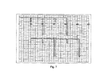
すべての試験において、180度のパルスパラメーターの位相シフトが用いられた。これは、逆パルスが試験パネルの片側で陽極に適用されたと同時に、順パルスが反対側で陽極に適用されたことを意味する。図7におけるパルス波形の図解(時間の相関要素である電流)は、上側陽極と下側陽極の間の位相シフトを示すこの設定を図解している(上側曲線:陰極の上側での電流、下側曲線:陰極の下側での電流)。 In all tests, a 180 degree pulse parameter phase shift was used. This means that a reverse pulse was applied to the anode on one side of the test panel and a forward pulse was applied to the anode on the opposite side. The illustration of the pulse waveform in FIG. 7 (current as a function of time) illustrates this setting showing the phase shift between the upper and lower anodes (upper curve: current above the cathode, lower Side curve: current under the cathode).
表2中に略述されている試験6で生産されたパネルの検鏡用薄切片の写真を、図8に示す。この事例では、3.0mm厚及び0.3mmのホール直径を有する10:1のアスペクト比のパネルが電気めっきされた。ホール中央で見ることが出来るように、達成された厚みは非常に少なく、Inpulse(登録商標)2システムでのパネルプレートは、およそ70%の均一電着性を有する。
A photograph of a thin section for microscopic examination of the panel produced in
類似したパネルと比較すると、わずか30%の均一電着性が、水平直流の3A/dm2で達成されるだろう。55%の均一電着性は直流の垂直条件下で、2A/dm2で達成される。空気攪拌を伴った標準的な垂直条件下でのパルスめっきだけで、90%の均一電着性が達成されるが、これは、2A/dm2の平均電流密度である。強制的な攪拌を用いて、均一電着性の向上は、以下に論じるように可能である。しかし、これでさえ、それほど高い電流密度でない。 Compared to similar panels, only 30% throwing power will be achieved at 3 A / dm 2 of horizontal direct current. A throwing power of 55% is achieved at 2 A / dm 2 under direct current vertical conditions. Only pulse plating under standard vertical conditions with air agitation achieves 90% throwing power, which is an average current density of 2 A / dm 2 . Using forced agitation, an improvement in throwing power is possible as discussed below. But even this is not a very high current density.
垂直適用
加工品の垂直めっきにおいて、上述の水平処理で述べた金属めっき電解液と同様の組成を持った金属めっき電解液が利用され得る。さらに、垂直めっきにおいて、パルスめっきは水平処理と同じ条件下で実施され得る。したがって、垂直めっきにおけるこれらのめっき条件に関しては、上述の説明が参照される。
Vertical application In the vertical plating of a processed product, a metal plating electrolyte having the same composition as the metal plating electrolyte described in the above-mentioned horizontal treatment can be used. Furthermore, in vertical plating, pulse plating can be performed under the same conditions as horizontal processing. Therefore, the above description is referred to regarding these plating conditions in the vertical plating.
垂直システムにおいて、電解液の攪拌は、通常、電解液自体における空気攪拌とめっきされる回路基板の機械的な攪拌の組合せでなされる。この機械的な攪拌は、パネルが一定に動かされ、且つ電解液中で垂直に保たれることを確実にしなければならない。さもなければ、溶液の流れは、パネル中の全てのホールを通って均一にならないであろう。この陰極の動作を確実にするために、パネルをしっかりと固定し、パネルに電流を供給するためにも使用されるシステムが用いられる。これらの攪拌システム、すなわち電解液中の空気及びパネルの動きは、明確でない(non-defined)空気攪拌のために、及び攪拌気泡を通るパネルの動作のために、不規則な流体搬送を引き起こし得る。 In vertical systems, electrolyte agitation is usually a combination of air agitation in the electrolyte itself and mechanical agitation of the circuit board being plated. This mechanical agitation must ensure that the panel is moved constantly and kept vertical in the electrolyte. Otherwise, the solution flow will not be uniform through all the holes in the panel. In order to ensure the operation of this cathode, a system is used which is also used to secure the panel and supply current to the panel. These agitation systems, ie air in the electrolyte and the movement of the panel, can cause irregular fluid transport due to non-defined air agitation and due to the operation of the panel through the agitation bubbles. .
これらの問題を克服するために、エゼクター(エダクタ:ベンチュリーの原理を用いるスプレーノズル、すなわち、作り出されたスプレーによって、ノズルを通過する追加的な流体の引き寄せが作用され、大容量流れが達成される)の使用がより一般的になっていく。ベンチュリーの原理を用いるエゼクターは、小さなポンプでより大容量の液体を循環する。或る溶液の運動エネルギーは、別の溶液の流れの原因となる。概して、エゼクターの使用は、ポンプ作用容量と比較したとき、溶液運動の容量において4〜6倍の増加を与えることが出来る。しかしながら、この増加容量は、直接にポンプ作用される溶液よりも低い圧力である。図9は、電気分解銅めっきシステムにおいて、一般的に用いられるエゼクターの二つの大きさを示している。示されている小さい方のエゼクターは、より少ない容量を送るが、より多くのエゼクターを一つの配管に設置することを許容し、よりむらのない電解液流れを与える。 To overcome these problems, ejectors (eductors: spray nozzles using the Venturi principle, i.e., the spray created, acts to draw additional fluid through the nozzles to achieve large volume flow. ) Is becoming more common. Ejectors that use the Venturi principle circulate larger volumes of liquid with a small pump. The kinetic energy of one solution causes the flow of another solution. In general, the use of an ejector can give a 4-6 fold increase in the volume of solution motion when compared to the pumping capacity. However, this increased volume is a lower pressure than the directly pumped solution. FIG. 9 shows two sizes of ejectors that are commonly used in electrolytic copper plating systems. The smaller ejector shown delivers less capacity, but allows more ejectors to be installed in one pipe, giving a more even electrolyte flow.
現在、垂直めっきタンク内のエゼクターの設置方法は、図10に示すように、陰極の下の床上にある。図10は、上側から下側までの眺めで垂直Inpulse(登録商標)ライン中のエゼクターの設備を示している。底部で、エゼクター9は供給配管10に配置される。
Currently, the installation method of the ejector in the vertical plating tank is on the floor under the cathode as shown in FIG. FIG. 10 shows the ejector installation in a vertical Inpulse® line with a top-to-bottom view. At the bottom, the ejector 9 is arranged in the
この設備は、陰極の下方で両側に一つずつおかれた二つの配管を有し、エゼクターが上向きに陰極の方を指し、もしくは陰極から離れるように向いて調整可能である。陰極のすぐ下で陰極に対して実質的に平行に伸びる単一配管に据えられたエゼクターを備える類似の設備、パネルから離れるように交互に向いた固定角で据えられたエゼクターを備える類似の設備がある。この設定に関する欠点は、電解液流れの均一性が、エゼクターの位置取り及びノズルとパネル間の距離の位置取りにも依存することである。 This installation has two pipes, one on each side below the cathode, and can be adjusted with the ejector pointing upwards or away from the cathode. Similar equipment with an ejector installed in a single pipe that extends substantially parallel to the cathode just below the cathode, similar equipment with ejectors installed at fixed angles that are alternately oriented away from the panel There is. The drawback with this setting is that the electrolyte flow uniformity also depends on the position of the ejector and the distance between the nozzle and the panel.
より均一な流れを与えるために、エゼクターは、めっきセル中で陰極の方へ真っ直ぐ向いている陽極の間に配置させることができる。この設定は、パネルに向かう電解液のより直進的な流れを与える利点を有し、設備の上側からその側方までの眺めとして図11に示されている。エゼクター9は、陽極11の前でタンクのそばに設置されているのが示されている。全てのエゼクター設備の欠点は、溶液の流れがパネル表面上で、決して完全に均一に出来ないことである。設置されるエゼクターの数と流れの均一性の間で、妥協させなければならない。 In order to provide a more uniform flow, the ejector can be placed between the anodes facing straight toward the cathode in the plating cell. This setting has the advantage of giving a more straight flow of electrolyte towards the panel and is shown in FIG. 11 as a view from the top of the facility to its side. The ejector 9 is shown installed beside the tank in front of the anode 11. The disadvantage of all ejector equipment is that the solution flow is never completely uniform on the panel surface. A compromise must be made between the number of ejectors installed and the flow uniformity.
エゼクターの使用による流れの均一性の制約を克服するために、移動スプレーシステムが開発され、実験室条件において試験タンク内で試験されている。本システムは、陰極表面の上を規則的に移動し、且つスプレーするときにパネルとスルーホールの強烈な強制されたあふれを生じさせるスプレーヘッドで構成される。ヘッドは、陽極と陰極の間を平面で移動し、パネルへ向いた方向で電解液を放出する。ヘッドは電着プロセスを妨げないような大きさで作られている。高アスペクト比のパネルを用いた結果では、標準的な空気攪拌と比較して、均一電着性において著しい改善が示され、同一規模でエゼクター攪拌装置と比べて、より均一な蒸着を示した。図12に、可動スプレーシステムを用いて、0.3mmのホールを有する3.0mmのパネル(アスペクト比10:1)のめっき結果を示す。電気めっきのための平均電流密度は、2A/dm2であった。均一電着性は、90〜95%になることが見出された。強化めっき(reinforcement plating)が、5A/dm2の電流密度で水平めっき装置において、直流めっきにより実施された。 In order to overcome the flow uniformity limitations due to the use of ejectors, mobile spray systems have been developed and tested in test tanks in laboratory conditions. The system consists of a spray head that moves regularly over the cathode surface and produces intense forced overflow of the panel and through-holes when spraying. The head moves in a plane between the anode and the cathode and discharges the electrolyte solution in a direction toward the panel. The head is sized so as not to interfere with the electrodeposition process. The results using the high aspect ratio panel showed a significant improvement in throwing power compared to standard air agitation, and more uniform deposition compared to the ejector agitator on the same scale. FIG. 12 shows the plating results of a 3.0 mm panel (aspect ratio 10: 1) having a 0.3 mm hole using a movable spray system. The average current density for the electroplating was 2A / dm 2. The throwing power was found to be 90-95%. Reinforcing plating (Reinforcement plating) is, in the horizontal plating apparatus at a current density of 5A / dm 2, was carried out by DC plating.
研究は、特に、5mmよりも厚いパネルにおいて、均一電着性を向上させるために、いわゆるバッチめっきパラメーターを使用して続けられている。めっき周期中に、パルスパラメーターは変化させられる。通常、周期の開始に強力な逆チャージが良好な均一電着性を与えるために用いられ、続いて、めっき周期の終了時に良好な表面仕上げを与えるためにより低い逆チャージが用いられる。そのような一連のめっきの例を、表4に示す。 Research continues, using so-called batch plating parameters to improve throwing power, especially in panels thicker than 5 mm. During the plating cycle, the pulse parameters are changed. Usually, a strong reverse charge is used at the beginning of the cycle to give good throwing power, followed by a lower reverse charge to give a good surface finish at the end of the plating cycle. An example of such a series of platings is shown in Table 4.
最適な電解液交換をもたらすための可動スプレーシステムと共に、改変されたパルスめっきシーケンスを用いた、0.5mmのホールを有する5.0mmのパネル(アスペクト比10:1)のめっき結果を図13に示す。使われた平均電流密度は、1.7A/dm2である。均一電着性は、95〜100%になることが見出された。 The plating results for a 5.0 mm panel (aspect ratio 10: 1) with 0.5 mm holes using a modified pulse plating sequence with a mobile spray system to provide optimal electrolyte exchange is shown in FIG. Show. The average current density used is 1.7 A / dm 2 . The throwing power was found to be 95-100%.
電解液攪拌と最適化されたパルスパラメーターの両方の使用は、試験ライン実験において、均一電着性における著しい改善をもたらす。 The use of both electrolyte agitation and optimized pulse parameters provides a significant improvement in throwing power in test line experiments.
したがって、基礎電気化学における実験は、銅電気めっき特性において電解液攪拌の強力な影響を示す。最適化されためっきパラメーターと共に水平Inpulse(登録商標)装置に対する改変は、実験条件下で改良された均一電着性を示す。 Thus, experiments in basic electrochemistry show a strong influence of electrolyte agitation on copper electroplating properties. Modifications to the horizontal Inpulse® device with optimized plating parameters show improved throwing power under experimental conditions.
垂直装置において、攪拌を改善するためのエゼクターの使用は、新しい装置にとって標準になっている。移動スプレーあふれシステム(moving spray flood system)の使用は、垂直システムにとって試験ライン規模において利点を示す。 In vertical equipment, the use of ejectors to improve agitation has become standard for new equipment. The use of a moving spray flood system offers advantages at the test line scale for vertical systems.
銅蒸着時間の間中、変化するパルスパラメーターの使用は、処理時間(周期時間)の終了時に、より穏やかなパルスパラメーターを用いて最適な表面仕上げを保持しながら、積極的なパラメーターで均一電着性を改善する可能性を提供する。 The use of pulse parameters that change throughout the copper deposition time allows uniform electrodeposition with aggressive parameters at the end of the treatment time (cycle time) while maintaining an optimal surface finish with a milder pulse parameter. Offer the possibility of improving sex.
技術手段による様々な改変と代替が、特許請求の範囲により規定されるような発明の範囲から逸脱することなく、上述の例と図により記載された内容に当て嵌められ得ることが理解されなければならない。さらに、本願に記載された特徴の様々な組合せが、当業者によって提案され、この発明の範囲内で且つ特許請求の範囲内に含まれることが理解されなければならない。この文書中に引用された全ての刊行物、特許及び特許出願は、参照することにより、結果として組み込まれる。 It should be understood that various modifications and alternatives by technical means may be applied to what is described by the above examples and figures without departing from the scope of the invention as defined by the claims. Don't be. Furthermore, it should be understood that various combinations of the features described in this application have been proposed by those skilled in the art and are included within the scope of the invention and the claims. All publications, patents and patent applications cited in this document are hereby incorporated by reference.
Claims (19)
a.加工品及び少なくとも一つの陽極と金属めっき電解液を接触させることと、
b.加工品と陽極の間に電圧を印加することで、その結果、電流の流れが加工品に生じ、そこで、電流の流れが、それぞれの周期時間中に、少なくとも一つの順電流パルスと少なくとも一つの逆電流パルスを有する最大でも約6Hzの周波数を有したパルス逆電流流れとなることを、備えて成る方法。 A method of electroplating a workpiece comprising a high aspect ratio hole comprising:
a. Contacting the workpiece and at least one anode with a metal plating electrolyte;
b. Applying a voltage between the workpiece and the anode results in a current flow in the workpiece, where the current flow is divided into at least one forward current pulse and at least one current during each cycle time. A method comprising providing a pulsed reverse current flow having a frequency of at most about 6 Hz with a reverse current pulse.
b.第二電圧を加工品の第二側面と少なくとも一つの第二陽極の間に印加し、その結果、各周期時間に少なくとも一つの第二順電流パルスと少なくとも一つの第二逆電流パルスの流れを有する第二パルス逆電流の流れが加工品の第二側面に生じることを備えて成る、請求項1〜6のいずれか一項に記載の方法。 a. A first voltage is applied between the first side of the workpiece and at least one first anode, so that at least one first forward current pulse and at least one first reverse current pulse flow at each cycle time. Having a first pulse reverse current flow on the first side of the workpiece;
b. A second voltage is applied between the second side of the workpiece and at least one second anode, so that at least one second forward current pulse and at least one second reverse current pulse flow at each cycle time. 7. A method according to any one of the preceding claims, wherein a second pulsed reverse current flow having occurs on the second side of the workpiece.
Applications Claiming Priority (2)
| Application Number | Priority Date | Filing Date | Title |
|---|---|---|---|
| DE10311575A DE10311575B4 (en) | 2003-03-10 | 2003-03-10 | Process for the electrolytic metallization of workpieces with high aspect ratio holes |
| PCT/EP2004/002208 WO2004081262A1 (en) | 2003-03-10 | 2004-02-04 | Method of electroplating a workpiece having high-aspect ratio holes |
Publications (2)
| Publication Number | Publication Date |
|---|---|
| JP2006519931A true JP2006519931A (en) | 2006-08-31 |
| JP2006519931A5 JP2006519931A5 (en) | 2007-05-24 |
Family
ID=32892263
Family Applications (1)
| Application Number | Title | Priority Date | Filing Date |
|---|---|---|---|
| JP2006504539A Ceased JP2006519931A (en) | 2003-03-10 | 2004-03-04 | Method of electroplating processed products having high aspect ratio holes |
Country Status (7)
| Country | Link |
|---|---|
| US (1) | US20060151328A1 (en) |
| EP (1) | EP1601822A1 (en) |
| JP (1) | JP2006519931A (en) |
| KR (1) | KR20050105280A (en) |
| DE (1) | DE10311575B4 (en) |
| TW (1) | TW200502443A (en) |
| WO (1) | WO2004081262A1 (en) |
Cited By (5)
| Publication number | Priority date | Publication date | Assignee | Title |
|---|---|---|---|---|
| JP2010095775A (en) * | 2008-10-20 | 2010-04-30 | Ebara-Udylite Co Ltd | Method for suppressing whisker in copper plating |
| JP2015503033A (en) * | 2011-12-21 | 2015-01-29 | アトテツク・ドイチユラント・ゲゼルシヤフト・ミツト・ベシユレンクテル・ハフツングAtotech Deutschland GmbH | Method for the combination of through-hole plating and via filling |
| US9376758B2 (en) | 2010-12-21 | 2016-06-28 | Ebara Corporation | Electroplating method |
| JP2018505960A (en) * | 2014-12-05 | 2018-03-01 | アトテック・ドイチュラント・ゲーエムベーハーAtotech Deutschland Gmbh | Method and apparatus for electroplating metal onto a substrate |
| WO2021245766A1 (en) * | 2020-06-02 | 2021-12-09 | 奥野製薬工業株式会社 | Intermittent electroplating method |
Families Citing this family (16)
| Publication number | Priority date | Publication date | Assignee | Title |
|---|---|---|---|---|
| US7553401B2 (en) * | 2004-03-19 | 2009-06-30 | Faraday Technology, Inc. | Electroplating cell with hydrodynamics facilitating more uniform deposition across a workpiece during plating |
| US7947161B2 (en) * | 2004-03-19 | 2011-05-24 | Faraday Technology, Inc. | Method of operating an electroplating cell with hydrodynamics facilitating more uniform deposition on a workpiece with through holes |
| DE102004045451B4 (en) * | 2004-09-20 | 2007-05-03 | Atotech Deutschland Gmbh | Galvanic process for filling through-holes with metals, in particular printed circuit boards with copper |
| US20070063521A1 (en) * | 2004-12-03 | 2007-03-22 | Lancashire Christopher L | Method and apparatus for plating automotive bumpers |
| DE502007005345D1 (en) * | 2006-03-30 | 2010-11-25 | Atotech Deutschland Gmbh | ELECTROLYTIC METHOD FOR FILLING HOLES AND DEEP WELLS WITH METALS |
| US8062496B2 (en) * | 2008-04-18 | 2011-11-22 | Integran Technologies Inc. | Electroplating method and apparatus |
| US20100206737A1 (en) * | 2009-02-17 | 2010-08-19 | Preisser Robert F | Process for electrodeposition of copper chip to chip, chip to wafer and wafer to wafer interconnects in through-silicon vias (tsv) |
| US9816193B2 (en) * | 2011-01-07 | 2017-11-14 | Novellus Systems, Inc. | Configuration and method of operation of an electrodeposition system for improved process stability and performance |
| KR101817823B1 (en) | 2011-01-26 | 2018-02-21 | 맥더미드 엔쏜 인코포레이티드 | Process for filling vias in the microelectronics |
| US9816196B2 (en) | 2012-04-27 | 2017-11-14 | Novellus Systems, Inc. | Method and apparatus for electroplating semiconductor wafer when controlling cations in electrolyte |
| US9435048B2 (en) * | 2013-02-27 | 2016-09-06 | Taiwan Semiconductor Manufacturing Co., Ltd. | Layer by layer electro chemical plating (ECP) process |
| DE102013021586A1 (en) * | 2013-12-19 | 2015-06-25 | Ludy Galvanosysteme Gmbh | Method and device for the electrochemical treatment of flat items to be treated |
| US10154598B2 (en) | 2014-10-13 | 2018-12-11 | Rohm And Haas Electronic Materials Llc | Filling through-holes |
| KR102619843B1 (en) * | 2018-12-28 | 2024-01-02 | 에이씨엠 리서치 (상하이), 인코포레이티드 | Plating device and plating method |
| CN110699725A (en) * | 2019-11-21 | 2020-01-17 | 上海江南轧辊有限公司 | In-liquid discharge deposition system and use method thereof |
| CN114554727A (en) * | 2022-03-31 | 2022-05-27 | 生益电子股份有限公司 | Electroplating method for realizing high-aspect-ratio through blind hole and PCB |
Family Cites Families (14)
| Publication number | Priority date | Publication date | Assignee | Title |
|---|---|---|---|---|
| CH629542A5 (en) * | 1976-09-01 | 1982-04-30 | Inoue Japax Res | METHOD AND DEVICE FOR GALVANIC MATERIAL DEPOSITION. |
| DE4134632C1 (en) * | 1991-10-19 | 1993-04-01 | Schering Ag Berlin Und Bergkamen, 1000 Berlin, De | |
| DE4225961C5 (en) * | 1992-08-06 | 2011-01-27 | Atotech Deutschland Gmbh | Apparatus for electroplating, in particular copper plating, flat plate or arched objects |
| DE4344387C2 (en) * | 1993-12-24 | 1996-09-05 | Atotech Deutschland Gmbh | Process for the electrolytic deposition of copper and arrangement for carrying out the process |
| DE19547948C1 (en) * | 1995-12-21 | 1996-11-21 | Atotech Deutschland Gmbh | Mfg. unipolar or bipolar pulsed current for plating esp. of circuit boards at high current |
| DE19717512C3 (en) * | 1997-04-25 | 2003-06-18 | Atotech Deutschland Gmbh | Device for electroplating circuit boards under constant conditions in continuous systems |
| US6071398A (en) * | 1997-10-06 | 2000-06-06 | Learonal, Inc. | Programmed pulse electroplating process |
| US6210555B1 (en) * | 1999-01-29 | 2001-04-03 | Faraday Technology Marketing Group, Llc | Electrodeposition of metals in small recesses for manufacture of high density interconnects using reverse pulse plating |
| DE19915146C1 (en) * | 1999-01-21 | 2000-07-06 | Atotech Deutschland Gmbh | Production of highly pure copper wiring trace on semiconductor wafer for integrated circuit by applying metal base coat, plating and structurization uses dimensionally-stable insoluble counter-electrode in electroplating |
| US6444110B2 (en) * | 1999-05-17 | 2002-09-03 | Shipley Company, L.L.C. | Electrolytic copper plating method |
| EP1069212A1 (en) * | 1999-07-12 | 2001-01-17 | Applied Materials, Inc. | Electrochemical deposition for high aspect ratio structures using electrical pulse modulation |
| US20040045832A1 (en) * | 1999-10-14 | 2004-03-11 | Nicholas Martyak | Electrolytic copper plating solutions |
| US6652727B2 (en) * | 1999-10-15 | 2003-11-25 | Faraday Technology Marketing Group, Llc | Sequential electrodeposition of metals using modulated electric fields for manufacture of circuit boards having features of different sizes |
| US6881318B2 (en) * | 2001-07-26 | 2005-04-19 | Applied Materials, Inc. | Dynamic pulse plating for high aspect ratio features |
-
2003
- 2003-03-10 DE DE10311575A patent/DE10311575B4/en not_active Expired - Fee Related
-
2004
- 2004-02-04 WO PCT/EP2004/002208 patent/WO2004081262A1/en not_active Application Discontinuation
- 2004-02-04 US US10/544,252 patent/US20060151328A1/en not_active Abandoned
- 2004-02-04 EP EP04707942A patent/EP1601822A1/en not_active Withdrawn
- 2004-02-04 KR KR1020057016921A patent/KR20050105280A/en not_active Application Discontinuation
- 2004-03-04 JP JP2006504539A patent/JP2006519931A/en not_active Ceased
- 2004-03-09 TW TW093106242A patent/TW200502443A/en unknown
Cited By (7)
| Publication number | Priority date | Publication date | Assignee | Title |
|---|---|---|---|---|
| JP2010095775A (en) * | 2008-10-20 | 2010-04-30 | Ebara-Udylite Co Ltd | Method for suppressing whisker in copper plating |
| US9376758B2 (en) | 2010-12-21 | 2016-06-28 | Ebara Corporation | Electroplating method |
| JP2015503033A (en) * | 2011-12-21 | 2015-01-29 | アトテツク・ドイチユラント・ゲゼルシヤフト・ミツト・ベシユレンクテル・ハフツングAtotech Deutschland GmbH | Method for the combination of through-hole plating and via filling |
| JP2018505960A (en) * | 2014-12-05 | 2018-03-01 | アトテック・ドイチュラント・ゲーエムベーハーAtotech Deutschland Gmbh | Method and apparatus for electroplating metal onto a substrate |
| US11015257B2 (en) | 2014-12-05 | 2021-05-25 | Atotech Deutschland Gmbh | Method and apparatus for electroplating a metal onto a substrate |
| WO2021245766A1 (en) * | 2020-06-02 | 2021-12-09 | 奥野製薬工業株式会社 | Intermittent electroplating method |
| WO2021246133A1 (en) * | 2020-06-02 | 2021-12-09 | 奥野製薬工業株式会社 | Intermittent electroplating method |
Also Published As
| Publication number | Publication date |
|---|---|
| KR20050105280A (en) | 2005-11-03 |
| DE10311575B4 (en) | 2007-03-22 |
| TW200502443A (en) | 2005-01-16 |
| WO2004081262A8 (en) | 2004-12-16 |
| EP1601822A1 (en) | 2005-12-07 |
| DE10311575A1 (en) | 2004-09-23 |
| US20060151328A1 (en) | 2006-07-13 |
| WO2004081262A1 (en) | 2004-09-23 |
Similar Documents
| Publication | Publication Date | Title |
|---|---|---|
| JP2006519931A (en) | Method of electroplating processed products having high aspect ratio holes | |
| JP5417112B2 (en) | Method for electrolytic deposition of metal layers | |
| EP1598449B1 (en) | Improved plating method | |
| US6071398A (en) | Programmed pulse electroplating process | |
| Hu et al. | Effects of deposition modes on the microstructure of copper deposits from an acidic sulfate bath | |
| US8329006B2 (en) | Electroplating cell with hydrodynamics facilitating more uniform deposition across a workpiece during plating | |
| CN101532160B (en) | Continuous copper electroplating method | |
| JPH04358091A (en) | Composition of electric plating solution | |
| JP5437665B2 (en) | High-speed continuous plating equipment | |
| JP2007277676A (en) | Electroplating method | |
| JP3352081B2 (en) | Printed circuit board copper plating equipment | |
| WO2003085713A1 (en) | Homogeneous copper-tin alloy plating for enhancement of electro-migration resistance in interconnects | |
| Ganesan et al. | Innovative advances in copper electroplating for IC Substrate manufacturing | |
| Kenny et al. | Plating High Aspect Ratio PCBs | |
| Qi-Xia | The effects of duty cycle and frequency on the crystal size of pulse-plated gold | |
| AU547410B2 (en) | Method for continuous metal deposition from a non- autocatalytic electroless plating bath using electric potential | |
| WO2023190805A1 (en) | Copper plating solution for pr pulse electrolysis and copper plating method by means of pr pulse electrolysis | |
| 김한 | Micro-pattern Metallization using Jet-circulating Electrodeposition | |
| JP2009074146A (en) | Method for producing black plated article |
Legal Events
| Date | Code | Title | Description |
|---|---|---|---|
| A072 | Dismissal of procedure [no reply to invitation to correct request for examination] |
Free format text: JAPANESE INTERMEDIATE CODE: A072 Effective date: 20060704 |
|
| A621 | Written request for application examination |
Free format text: JAPANESE INTERMEDIATE CODE: A621 Effective date: 20070302 |
|
| A521 | Request for written amendment filed |
Free format text: JAPANESE INTERMEDIATE CODE: A523 Effective date: 20070328 |
|
| A977 | Report on retrieval |
Free format text: JAPANESE INTERMEDIATE CODE: A971007 Effective date: 20090518 |
|
| A01 | Written decision to grant a patent or to grant a registration (utility model) |
Free format text: JAPANESE INTERMEDIATE CODE: A01 Effective date: 20090526 |
|
| A045 | Written measure of dismissal of application [lapsed due to lack of payment] |
Free format text: JAPANESE INTERMEDIATE CODE: A045 Effective date: 20090929 |