JP2006236105A - アクセス制御装置及びその制御方法 - Google Patents
アクセス制御装置及びその制御方法 Download PDFInfo
- Publication number
- JP2006236105A JP2006236105A JP2005051369A JP2005051369A JP2006236105A JP 2006236105 A JP2006236105 A JP 2006236105A JP 2005051369 A JP2005051369 A JP 2005051369A JP 2005051369 A JP2005051369 A JP 2005051369A JP 2006236105 A JP2006236105 A JP 2006236105A
- Authority
- JP
- Japan
- Prior art keywords
- memory
- access
- memory module
- address
- area
- Prior art date
- Legal status (The legal status is an assumption and is not a legal conclusion. Google has not performed a legal analysis and makes no representation as to the accuracy of the status listed.)
- Withdrawn
Links
Images


Classifications
-
- G—PHYSICS
- G06—COMPUTING OR CALCULATING; COUNTING
- G06F—ELECTRIC DIGITAL DATA PROCESSING
- G06F12/00—Accessing, addressing or allocating within memory systems or architectures
- G06F12/02—Addressing or allocation; Relocation
- G06F12/06—Addressing a physical block of locations, e.g. base addressing, module addressing, memory dedication
- G06F12/0646—Configuration or reconfiguration
-
- G—PHYSICS
- G06—COMPUTING OR CALCULATING; COUNTING
- G06F—ELECTRIC DIGITAL DATA PROCESSING
- G06F12/00—Accessing, addressing or allocating within memory systems or architectures
- G06F12/02—Addressing or allocation; Relocation
- G06F12/0215—Addressing or allocation; Relocation with look ahead addressing means
Landscapes
- Engineering & Computer Science (AREA)
- Theoretical Computer Science (AREA)
- Physics & Mathematics (AREA)
- General Engineering & Computer Science (AREA)
- General Physics & Mathematics (AREA)
- Dram (AREA)
- Memory System (AREA)
- Techniques For Improving Reliability Of Storages (AREA)
Priority Applications (3)
| Application Number | Priority Date | Filing Date | Title |
|---|---|---|---|
| JP2005051369A JP2006236105A (ja) | 2005-02-25 | 2005-02-25 | アクセス制御装置及びその制御方法 |
| US11/345,388 US20060195665A1 (en) | 2005-02-25 | 2006-02-02 | Access control device, method for changing memory addresses, and memory system |
| CNA2006100078923A CN1825473A (zh) | 2005-02-25 | 2006-02-23 | 存储器控制装置、改变存储器地址的方法以及存储系统 |
Applications Claiming Priority (1)
| Application Number | Priority Date | Filing Date | Title |
|---|---|---|---|
| JP2005051369A JP2006236105A (ja) | 2005-02-25 | 2005-02-25 | アクセス制御装置及びその制御方法 |
Publications (2)
| Publication Number | Publication Date |
|---|---|
| JP2006236105A true JP2006236105A (ja) | 2006-09-07 |
| JP2006236105A5 JP2006236105A5 (https=) | 2008-04-10 |
Family
ID=36933127
Family Applications (1)
| Application Number | Title | Priority Date | Filing Date |
|---|---|---|---|
| JP2005051369A Withdrawn JP2006236105A (ja) | 2005-02-25 | 2005-02-25 | アクセス制御装置及びその制御方法 |
Country Status (3)
| Country | Link |
|---|---|
| US (1) | US20060195665A1 (https=) |
| JP (1) | JP2006236105A (https=) |
| CN (1) | CN1825473A (https=) |
Cited By (2)
| Publication number | Priority date | Publication date | Assignee | Title |
|---|---|---|---|---|
| JP2011530734A (ja) * | 2008-08-08 | 2011-12-22 | ヒューレット−パッカード デベロップメント カンパニー エル.ピー. | 標準メモリモジュールとピン互換性のあるメモリモジュール内における独立制御可能且つ再構成可能な仮想メモリデバイス |
| US8867294B2 (en) | 2010-03-12 | 2014-10-21 | Ps4 Luxco S.A.R.L. | Semiconductor device, refresh control method thereof and computer system |
Families Citing this family (5)
| Publication number | Priority date | Publication date | Assignee | Title |
|---|---|---|---|---|
| US7904639B2 (en) * | 2006-08-22 | 2011-03-08 | Mosaid Technologies Incorporated | Modular command structure for memory and memory system |
| JP2008242731A (ja) * | 2007-03-27 | 2008-10-09 | Oki Electric Ind Co Ltd | マイクロプロセッサ設計プログラム、マイクロプロセッサ設計装置及びマイクロプロセッサ |
| JP5171448B2 (ja) * | 2007-07-31 | 2013-03-27 | キヤノン株式会社 | 画像形成装置及びその制御方法 |
| JP2011081732A (ja) * | 2009-10-09 | 2011-04-21 | Elpida Memory Inc | 半導体装置及びその調整方法並びにデータ処理システム |
| CN111158600B (zh) * | 2019-12-30 | 2023-10-27 | 中国人民解放军国防科技大学 | 一种提升高带宽存储器(hbm)访问效率的装置和方法 |
Family Cites Families (3)
| Publication number | Priority date | Publication date | Assignee | Title |
|---|---|---|---|---|
| US6571325B1 (en) * | 1999-09-23 | 2003-05-27 | Rambus Inc. | Pipelined memory controller and method of controlling access to memory devices in a memory system |
| JP4159415B2 (ja) * | 2002-08-23 | 2008-10-01 | エルピーダメモリ株式会社 | メモリモジュール及びメモリシステム |
| US7222224B2 (en) * | 2004-05-21 | 2007-05-22 | Rambus Inc. | System and method for improving performance in computer memory systems supporting multiple memory access latencies |
-
2005
- 2005-02-25 JP JP2005051369A patent/JP2006236105A/ja not_active Withdrawn
-
2006
- 2006-02-02 US US11/345,388 patent/US20060195665A1/en not_active Abandoned
- 2006-02-23 CN CNA2006100078923A patent/CN1825473A/zh active Pending
Cited By (4)
| Publication number | Priority date | Publication date | Assignee | Title |
|---|---|---|---|---|
| JP2011530734A (ja) * | 2008-08-08 | 2011-12-22 | ヒューレット−パッカード デベロップメント カンパニー エル.ピー. | 標準メモリモジュールとピン互換性のあるメモリモジュール内における独立制御可能且つ再構成可能な仮想メモリデバイス |
| KR101477849B1 (ko) * | 2008-08-08 | 2014-12-30 | 휴렛-팩커드 디벨롭먼트 컴퍼니, 엘.피. | 메모리 모듈 및 메모리 모듈 제어 방법 |
| US8924639B2 (en) | 2008-08-08 | 2014-12-30 | Hewlett-Packard Development Company, L.P. | Independently controllable and reconfigurable virtual memory devices in memory modules that are pin-compatible with standard memory modules |
| US8867294B2 (en) | 2010-03-12 | 2014-10-21 | Ps4 Luxco S.A.R.L. | Semiconductor device, refresh control method thereof and computer system |
Also Published As
| Publication number | Publication date |
|---|---|
| US20060195665A1 (en) | 2006-08-31 |
| CN1825473A (zh) | 2006-08-30 |
Similar Documents
| Publication | Publication Date | Title |
|---|---|---|
| US5835435A (en) | Method and apparatus for dynamically placing portions of a memory in a reduced power consumtion state | |
| KR100281432B1 (ko) | 플래쉬 메모리에 기초한 주메모리 | |
| US12346608B2 (en) | Asynchronous arbitration across clock domains for register writes in an integrated circuit chip | |
| US20180275921A1 (en) | Storage device | |
| US20050289317A1 (en) | Method and related apparatus for accessing memory | |
| US20080285372A1 (en) | Multi- port memory device for buffering between hosts and non-volatile memory devices | |
| JP2011040041A (ja) | 書き込みレベリング動作を行うためのメモリ装置の制御方法、メモリ装置の書き込みレベリング方法、及び書き込みレベリング動作を行うメモリコントローラ、メモリ装置、並びにメモリシステム | |
| JP2008305350A (ja) | メモリシステム、メモリ装置、およびメモリ装置の制御方法 | |
| JP2009086702A (ja) | メモリ制御装置および半導体装置 | |
| JP5188134B2 (ja) | メモリアクセス制御装置及びメモリアクセス制御方法 | |
| JP2006313538A (ja) | メモリモジュール及びメモリシステム | |
| US8433835B2 (en) | Information processing system and control method thereof | |
| JP2004536417A (ja) | 読出及び書込動作でバースト順序が異なるアドレッシングを行うメモリデバイス | |
| WO2023107304A1 (en) | Read clock start and stop for synchronous memories | |
| JP2014154119A (ja) | メモリ制御装置及び半導体記憶装置 | |
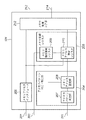
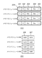
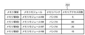
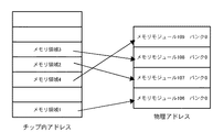
| JP2006236105A (ja) | アクセス制御装置及びその制御方法 | |
| JP5349775B2 (ja) | メモリコントローラ及びその制御方法 | |
| JP2000194596A (ja) | メモリ制御装置、キャッシュ装置、メモリ制御システムおよび方法、記録媒体 | |
| CN114253464B (zh) | 控制读取请求的方法和具有主机装置的存储器控制器 | |
| KR20240081027A (ko) | 어드레스 디코딩 방법, 및 이를 이용한 메모리 컨트롤러 및 반도체 메모리 시스템 | |
| JP6170363B2 (ja) | 制御装置、コンピュータシステム、制御方法、及びプログラム | |
| JP2006146340A (ja) | メモリ制御装置及びメモリ制御方法 | |
| JP2006146817A (ja) | メモリ制御システム及びメモリ制御装置 | |
| JP3956698B2 (ja) | メモリ制御装置 | |
| JP2008040896A (ja) | メモリ制御装置及びメモリ制御方法 |
Legal Events
| Date | Code | Title | Description |
|---|---|---|---|
| A521 | Written amendment |
Free format text: JAPANESE INTERMEDIATE CODE: A523 Effective date: 20080221 |
|
| A621 | Written request for application examination |
Free format text: JAPANESE INTERMEDIATE CODE: A621 Effective date: 20080221 |
|
| A761 | Written withdrawal of application |
Free format text: JAPANESE INTERMEDIATE CODE: A761 Effective date: 20090821 |