JP2006135013A - Mounting device and mounting method - Google Patents
Mounting device and mounting method Download PDFInfo
- Publication number
- JP2006135013A JP2006135013A JP2004320748A JP2004320748A JP2006135013A JP 2006135013 A JP2006135013 A JP 2006135013A JP 2004320748 A JP2004320748 A JP 2004320748A JP 2004320748 A JP2004320748 A JP 2004320748A JP 2006135013 A JP2006135013 A JP 2006135013A
- Authority
- JP
- Japan
- Prior art keywords
- chip
- area
- image
- wafer
- wafer table
- Prior art date
- Legal status (The legal status is an assumption and is not a legal conclusion. Google has not performed a legal analysis and makes no representation as to the accuracy of the status listed.)
- Pending
Links
Images


Landscapes
- Die Bonding (AREA)
Abstract
Description
この発明は実装装置及び実装方法に関する。更に、具体的には、半導体チップをリードフレームやパッケージ等の基板に装着する際に用いる実装装置及び実装方法に関するものである。 The present invention relates to a mounting apparatus and a mounting method. More specifically, the present invention relates to a mounting apparatus and a mounting method used when a semiconductor chip is mounted on a substrate such as a lead frame or a package.
一般に、半導体装置の製造工程において、例えば、ウェハから切り出された半導体チップを、リードフレームに装着(ボンディング)する場合、ダイボンディング装置が用いられる。ダイボンディング装置では、ウェハテーブル上に、複数のチップが形成されそれぞれがダイシングされた状態のウェハが載置される。そして、ウェハから、1のチップを、ピックアップユニットによりピックアップする。このとき、ウェハ下面側からは、ピックアップされるチップが、突出ユニットにより突き出される。そして、ピックアップされたチップは、別の場所に準備されたリードフレームの所定の位置まで移動され、リードフレームにボンディングされる。 Generally, in a semiconductor device manufacturing process, for example, when a semiconductor chip cut out from a wafer is mounted (bonded) to a lead frame, a die bonding apparatus is used. In a die bonding apparatus, a wafer in which a plurality of chips are formed and diced is placed on a wafer table. Then, one chip is picked up from the wafer by the pickup unit. At this time, the chip to be picked up is projected from the lower surface side of the wafer by the protruding unit. Then, the picked-up chip is moved to a predetermined position of a lead frame prepared in another place and bonded to the lead frame.
このような装置においては、突出ユニットが設けられた位置の上部に、ボンディングの対象となるチップが配置されるように、ウェハを、ウェハテーブルにより移動させる。そして、ピックアップユニットを下方に動かしてチップをピックアップして、リードフレームに装着する。 In such an apparatus, the wafer is moved by the wafer table so that the chip to be bonded is disposed above the position where the protruding unit is provided. Then, the chip is picked up by moving the pickup unit downward and mounted on the lead frame.
ところで、このような装置を用いる場合、ウェハが大口径化するにつれて、ウェハテーブルを大きくし、また、ウェハテーブルの稼動範囲も大きくしなければならない。従って、ウェハの大口径化に伴い、ダイボンディング装置も大型化してしまう。しかし、装置の大型化は、半導体装置の製造に大きなスペースを必要とし、コストの増大等を招くため問題となる。 By the way, when such an apparatus is used, the wafer table must be enlarged and the operating range of the wafer table must be increased as the wafer diameter increases. Therefore, the die bonding apparatus is also increased in size as the wafer diameter increases. However, the increase in the size of the device is a problem because it requires a large space for manufacturing the semiconductor device and causes an increase in cost.
従って、ウェハが、4インチ(101.6mm)、5インチ(127mm)と大口径化するのに備えて、従来の小型のダイボンディング装置を改良して用いるようにする技術が考えられている。 Therefore, a technique for improving the conventional small die bonding apparatus in preparation for increasing the diameter of the wafer to 4 inches (101.6 mm) and 5 inches (127 mm) has been considered.
この技術では、ウェハを、ウェハの中心を通り、90度に直行する2本の直線により、4つのエリアに分割して、1つのエリアの全チップをボンディングした後、ウェハテーブルを90度回転させ、隣のエリアの全半導体チップをボンディングする。これを繰り返すことにより、4つのエリアの全チップのボンディングを行うことができるようにしている。このようにすることにより、ウェハテーブルは、ウェハの1/4の距離を移動することができればよく、従って、従来の装置を改良して、小型の装置のまま、半導体チップのボンディングを行うことができる(例えば、特許文献1参照)。 In this technique, a wafer is divided into four areas by two straight lines passing through the center of the wafer and orthogonal to 90 degrees, and after bonding all chips in one area, the wafer table is rotated 90 degrees. Bond all semiconductor chips in the adjacent area. By repeating this, bonding of all chips in the four areas can be performed. By doing so, the wafer table only needs to be able to move a distance of 1/4 of the wafer. Therefore, the conventional apparatus can be improved and semiconductor chips can be bonded with a small apparatus. (For example, refer to Patent Document 1).
しかしながら、ウェハは、更に大口径化が進み、現在では、8インチウェハ、あるいはそれ以上のウェハの処理を考える必要がある。従って、4インチより前の世代の小型の装置を4インチ、5インチ用に改良した技術では、対応することができない。 However, the diameter of the wafer has further increased, and it is now necessary to consider processing of an 8-inch wafer or more. Therefore, it is not possible to cope with a technology in which a small-sized device of a generation before 4 inches is improved for 4 inches and 5 inches.
また、ウェハの大口径に対して、チップ内のパターンは微細化が進み、ボンディングにおいても、正確な位置合わせが要求される。従って、ウェハテーブルを回転させる技術だけでは、チップのボンディング位置にズレが生じることが考えられるため、問題となる。 Further, with respect to the large diameter of the wafer, the pattern in the chip has been miniaturized, and accurate alignment is required also in bonding. Therefore, it is considered that the technique of rotating the wafer table alone may cause a deviation in the bonding position of the chip, which is a problem.
また、1のウェハ内に形成されるチップの枚数、あるいは各チップの形状も、多様化している。しかし、上述したウェハの中心を通る中心線で、4つのエリアに分ける方法では、ウェハ上のチップ枚数が奇数の場合に適用することができない。即ち、奇数枚の場合、その中心線が、チップの中央を通ることになり、その中心線上にあるチップのボンディングができないことになる。あるいは、チップが偶数の場合であっても、チップサイズがウェハ面内で全て均一であるとは限らず、この場合、ウェハの中心線が、チップ上に乗ることも考えられる。 Also, the number of chips formed in one wafer or the shape of each chip is diversified. However, the above-described method of dividing into four areas by the center line passing through the center of the wafer cannot be applied when the number of chips on the wafer is an odd number. That is, in the case of an odd number, the center line passes through the center of the chip, and the chip on the center line cannot be bonded. Alternatively, even when the number of chips is an even number, the chip size is not always uniform within the wafer surface. In this case, the center line of the wafer may be placed on the chip.
従って、この発明は、ウェハが大型化する場合にも、実装装置自体の大型化を抑えつつ、かつ、ウェハ面内に、多種類のチップが形成されているような場合でも、正確にチップをボンディングすることができるように改良した実装装置及び実装方法を提案するものである。 Therefore, the present invention suppresses the increase in size of the mounting apparatus itself even when the wafer is increased in size, and even when a large variety of chips are formed in the wafer surface, the chip can be accurately positioned. The present invention proposes a mounting apparatus and a mounting method improved so that bonding can be performed.
この発明の実装装置は、ウェハ内の複数個に分割されたチップを保持し、基板に装着する実装装置である。この実装装置は、前記ウェハを載置するウェハテーブルと、前記ウェハテーブルに載置された前記ウェハ内の複数のチップのいずれかを押し上げる突上部と、前記突上部に押し上げられたチップを保持して、前記基板上に移動する保持部とを備える。また、前記ウェハテーブルは、前記ウェハ内の複数のチップのうち、装着の対象となるチップが、前記突上部上方に位置するように、所定の移動範囲内で、前記ウェハを移動させる駆動機構を備える。また、ウェハテーブルは、前記ウェハ面内を、前記ウェハの中心付近にあるチップを中心チップとして、前記中心チップの4辺を、それぞれ一方向に、かつ、対向する2辺については互いに別の方向に、延びるように延長させた延長線により4つのエリアに分けた場合に、前記エリアのうちいずれか1のエリアが、前記ウェハテーブルの前記所定の移動範囲内に位置するように、前記ウェハテーブルを基準位置から所定の角度回転させるテーブル回転機構を備える。 The mounting apparatus according to the present invention is a mounting apparatus for holding a chip divided into a plurality of pieces in a wafer and mounting the chip on a substrate. The mounting apparatus holds a wafer table on which the wafer is mounted, a protruding portion that pushes up any one of the plurality of chips placed on the wafer table, and a chip that is pushed up on the protruding portion. And a holding portion that moves on the substrate. The wafer table has a drive mechanism for moving the wafer within a predetermined movement range so that a chip to be mounted among the plurality of chips in the wafer is located above the protrusion. Prepare. The wafer table has a chip located near the center of the wafer as a central chip within the wafer surface, each of the four sides of the central chip in one direction, and two opposing sides in different directions. When the wafer table is divided into four areas by extension lines extended so as to extend, the wafer table is arranged such that any one of the areas is located within the predetermined movement range of the wafer table. Is provided with a table rotation mechanism for rotating the lens at a predetermined angle from the reference position.
また、この発明の実装方法は、複数のチップが形成されたウェハをウェハテーブルに載置し、保持部により1のチップを取り上げ、基板に装着する実装方法である。この実装方法においては、前記ウェハの中心付近の1のチップを中心チップとして選択し、前記中心チップの4辺を、それぞれ一方向に、かつ、対向する2辺については互いに別の方向に、延びるように延長させた延長線により、前記ウェハ面内を、前記中心チップに接する中心角が90度である第1、第2、第3、第4エリアに分割する。そして、前記第1エリアが、前記ウェハテーブルの所定の移動範囲内に配置されるようにして、前記1エリア内の前記チップを、それぞれ、前記保持部により前記基板に装着する。その後、前記ウェハテーブルを90度回転させて前記第2エリアが前記所定の移動範囲内に配置されるよう前記第2エリア内の前記各チップを、前記保持部により保持した状態で前記ウェハテーブルの回転と逆の方向に90度回転させて、前記基板に装着する。また、その後、前記ウェハテーブルを90度回転させて、前記第3エリアが前記所定の移動範囲内に配置されるようにし、前記第3エリア内の前記各チップを、前記保持部により保持した状態で前記ウェハテーブルの回転と逆の方向に180度回転させて、前記基板に装着する。また、その後、前記ウェハテーブルを90度回転させて、前記第4エリアが前記所定の移動範囲内に配置されるようにし、前記第4エリア内の前記各チップを、前記保持部により保持した状態で前記ウェハテーブルの回転と逆の方向に270度回転させ、前記基板に装着する。そして、前記中心チップを、前記保持部により保持した状態で前記ウェハテーブルの回転と逆の方向に270度回転させ、前記保持部により前記基板に装着する。 The mounting method of the present invention is a mounting method in which a wafer on which a plurality of chips are formed is placed on a wafer table, one chip is picked up by a holding portion, and is mounted on a substrate. In this mounting method, one chip in the vicinity of the center of the wafer is selected as a central chip, and four sides of the central chip are extended in one direction and two opposite sides are extended in different directions. The wafer surface is divided into first, second, third, and fourth areas having a central angle of 90 degrees in contact with the central chip by the extended lines extended in this manner. Then, each of the chips in the one area is mounted on the substrate by the holding unit such that the first area is disposed within a predetermined movement range of the wafer table. Thereafter, the wafer table is rotated by 90 degrees, and the respective chips in the second area are held by the holding unit so that the second area is disposed within the predetermined movement range. The substrate is rotated by 90 degrees in the opposite direction to the rotation and mounted on the substrate. Thereafter, the wafer table is rotated by 90 degrees so that the third area is disposed within the predetermined movement range, and the chips in the third area are held by the holding unit. Then, the wafer table is rotated 180 degrees in the direction opposite to the rotation of the wafer table and mounted on the substrate. Thereafter, the wafer table is rotated by 90 degrees so that the fourth area is disposed within the predetermined movement range, and the chips in the fourth area are held by the holding unit. Then, the wafer table is rotated by 270 degrees in the opposite direction to the rotation of the wafer table and mounted on the substrate. Then, the central chip is rotated by 270 degrees in the direction opposite to the rotation of the wafer table while being held by the holding unit, and is mounted on the substrate by the holding unit.
この発明においては、実装装置は、ウェハ面内の中心付近にあるチップを中心チップとして、中心チップの各辺を、それぞれ一方向に、かつ、互いに対向する2辺については逆方向に、延長した延長線により、ウェハを4つのエリアに分割する。そして、ウェハを回転させて、各エリアごとにチップのボンディングを行う。従って、従来の実装装置のウェハテーブルの、突出部に対する移動量を、ウェハの1/4程度の距離に抑えることができる。また、中心チップを選択し、これを中心とするため、ウェハ面内に奇数のチップが形成されている場合や、形状の異なるチップが形成されている場合にも、確実に全てのチップのボンディングを行うことができる。従って、ウェハが大口径化し、かつ、多用化する場合にも、装置の大型化を抑えることができる。 In the present invention, the mounting device extends a chip near the center in the wafer surface as a central chip, and each side of the central chip extends in one direction and in opposite directions with respect to two opposite sides. The extension line divides the wafer into four areas. Then, the wafer is rotated to perform chip bonding for each area. Therefore, the movement amount of the wafer table of the conventional mounting apparatus with respect to the protruding portion can be suppressed to a distance of about 1/4 of the wafer. Also, since the center chip is selected and centered, even when odd-numbered chips are formed in the wafer surface or when chips having different shapes are formed, bonding of all chips is ensured. It can be performed. Therefore, even when the wafer has a large diameter and is diversified, an increase in the size of the apparatus can be suppressed.
以下、図面を参照して本発明の実施の形態について説明する。なお、各図において、同一または相当する部分には同一符号を付してその説明を簡略化ないし省略する。
また、以下の実施の形態において各要素の個数、数量、量、範囲等の数に言及する場合、特に明示した場合や原理的に明らかにその数に特定される場合を除いて、その言及した数に限定されるものではない。また、実施の形態において説明する構造や、方法におけるステップ等は、特に明示した場合や明らかに原理的にそれに特定される場合を除いて、この発明に必ずしも必須のものではない。
Embodiments of the present invention will be described below with reference to the drawings. In the drawings, the same or corresponding parts are denoted by the same reference numerals, and the description thereof is simplified or omitted.
In addition, in the following embodiments, when referring to the number of each element, quantity, quantity, range, etc., the reference is made unless otherwise specified or the number is clearly specified in principle. The number is not limited. Further, the structures described in the embodiments, steps in the method, and the like are not necessarily essential to the present invention unless otherwise specified or clearly specified in principle.
実施の形態1.
図1は、この発明の実施の形態1におけるダイボンディング装置を説明するための模式図である。また、図2は、実施の形態1におけるダイボンディング装置において処理するウェハについて説明するための上面図である。
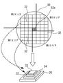
図1を参照して、ダイボンディング装置100において、ウェハテーブル2の上方には、認識カメラ4及びピックアップユニット6が設けられ、ウェハテーブル2の下方には、突上ユニット4が設置されている。
FIG. 1 is a schematic diagram for explaining a die bonding apparatus according to
Referring to FIG. 1, in die bonding apparatus 100,
ウェハテーブル2は、回転軸を中心に回転することができる。また、X方向、Y方向、Z方向への移動を行うことでき、これにより、ウェハの位置合わせを行うことができる。
認識カメラ4は、ウェハテーブル2上のチップの画像を必要に応じて取得することができる。
The wafer table 2 can rotate around a rotation axis. Further, movement in the X direction, the Y direction, and the Z direction can be performed, whereby the wafer can be aligned.
The
ピックアップユニット6は、吸着部10と回転軸12とを有する。吸着部10は、回転軸12により回転軸12の中心軸を中心として回転することができる。また、ピックアップユニット6は、後述するが所定の範囲内を移動することができる。
The
突上ユニット8は、回転軸14により、回転軸14の中心軸を中心に回転することができる。但し、ボンディング処理中、突上ユニット4の回転の中心軸は、X、Y方向には移動することはなく、固定された位置において回転し、あるいは、Z方向の上下移動を行うのみである。
The
ウェハテーブル2とピックアップユニット6の回転軸12と突上ユニット8の回転軸14とは、それぞれ、駆動手段16に接続されている。駆動手段16は、回転軸12、14及びウェハテーブル2を回転させることができる。また、駆動手段16及び認知カメラ4は、共に、制御手段18に接続されている。
また、ウェハテーブル2とは異なる場所に、リードフレーム台20が設けられている。
The
In addition, a
このように構成されたダイボンディング装置を用いてボンディングを行う場合、ウェハテーブル2には、ウェハ30が載置される。このとき、ウェハ30は、粘着シートが取り付けられた状態で、複数のチップ32にダイシングされている。また、リードフレーム台20には、チップ32を搭載するためのリードフレーム34が配置される。
When bonding is performed using the die bonding apparatus configured as described above, the
ダイボンディング装置は、ウェハ30上のチップ32を、ピックアップユニット6により、1つずつピックアップして、リードフレーム台20のリードフレーム34上にボンディングする。この実施の形態1においては、ウェハ30を4つのエリアに分けて、エリアごとの処理を行う。
The die bonding apparatus picks up
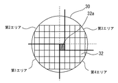
具体的には、図2に示すように、ウェハ30の中心付近にあるチップを、中心チップ32aとして決定する。そして、この中心チップ32aの4辺をそれぞれ1方向に、かつ、対向する2辺については互いに逆の方向に延ばした延長線により、ウェハ30面内を4つのエリアに分割する。即ち、ウェハ30面内は、上面から見て、各エリアの中心角が90度の扇形状の4エリアに分割され、ウェハ30内の中心チップ32aを除く全てのチップ32は、4つのエリアのいずれかに含まれる。実施の形態1においては、図2における左右の辺を、それぞれ、下、上方向に伸ばし、上下の辺を、それぞれ、左、右方向に伸ばした線により、4つのエリアに分割している。なお、以下、実施の形態1〜4においては、ウェハ30の、図2における左下、左上、右下、右上のエリアを、それぞれ、第1、第2、第3、第4エリアと称することとする。
Specifically, as shown in FIG. 2, the chip near the center of the
ウェハテーブル2は、Z方向の移動によりウェハテーブル2の高さ及び傾きを調節し、かつ、XY方向に移動する。ウェハテーブル2の移動範囲は、ウェハの第1〜第4エリアの各エリア内に形成されている全てのチップ32について、その中心が、ウェハテーブル2の移動により、突上ユニット8上に位置するようにできる範囲である。なお、以下、簡略化のため、ウェハステージ2の移動により突上げユニット8上に位置するようにできる範囲を、「処理範囲」と称することとする。
また、認識カメラ4は、ウェハステージ2の処理範囲内のボンディング対象となっているチップ32の画像を認識することができる。なお、以下簡略化のため、ボンディング対象となっているチップを、「対象チップ」と称することとする。
The wafer table 2 adjusts the height and inclination of the wafer table 2 by moving in the Z direction, and moves in the XY direction. The movement range of the wafer table 2 is such that the center of all the
Further, the
認識カメラ4により、第1〜第4エリアのうち対象チップの画像が認識されると、この画像が制御手段18に送られる。そして、制御手段18により、予め登録されたそのチップ32の位置合わせの基準となるテンプレート画像と比較して、ボンディングされるチップ32の中心が、突上ユニット8の直上、かつ、ピックアップユニット6の直下にくるように、ウェハテーブル2の移動量が算出される。この算出結果により、駆動手段16は、ウェハテーブル2のXY方向への移動による位置合わせを行う。
When the
また、実施の形態1では、ウェハテーブル2は、90度毎の回転を行うことができる。この回転は、ウェハ30上の中心チップ32aの中心を中心に行う。実際のボンディングの際には、ウェハ30を載置する際には、まず第1エリアから順に、チップの装着処理が行われるようにウェハ30を載置して位置合わせが行われる。そして、第1エリア内のチップ32が、順に処理された後、ウェハテーブル2は、中心チップ32aの中心を中心として、左周りに90度回転する。このようにすると、第2エリアが、ウェハステージ2の処理範囲に移動することになる。このように、ウェハテーブル2の90度ごとの回転を続けることにより、第1〜第4エリアの全ての処理を行うことができるようになっている。
In the first embodiment, the wafer table 2 can rotate every 90 degrees. This rotation is performed around the center of the
また、ピックアップユニット6は、吸着部10により、所定のチップ32をピックアップすることができる。ピックアップするチップ32は、ウェハテーブル2のXY方向の移動により、常に、ピックアップユニット6の直下に位置するようになっている。また、ピックアップユニット6は、回転軸12を中心として回転することができ、これにより、チップ32のウェハテーブル2の回転による位置のズレを、元に戻す方向に、チップ32を回転させることができる。ピックアップユニット6のピックアップ時の動作は、基本的に上下移動と、回転軸12を中心とした回転のみである。
Further, the
また、突上ユニット8は、ピックアップユニット6によるピックアップの動作を補助する。即ち、突上げユニット8は上方に位置するチップ32を下から押し上げる。そして、ピックアップユニット6により、突き上げられたチップ32が、ピックアップユニット6の吸着部10に吸着されて保持されることになる。また、突上ユニット8は、基本的に位置を変えず、ウェハテーブル30がXY方向に移動することにより、突上げユニット8直上に、ボンディング対象のチップ32が配置されるようにする。従って、突上ユニット8の突上げ時の動作も基本的には上下方向のみであるが、突上ユニット8は、回転軸14を中心として、回転を行うことができるようになっている。
Further, the
また、制御手段18は、上述したようにウェハテーブル2及びピックアップユニット6、突上ユニット8の移動や回転を制御する。また、制御手段18には、各チップ32移動時の位置合わせの際に基準となる、テンプレート画像が、各エリアごとに、チップ32のパターンの種類に応じて登録されている。また、中心チップ32aは、全てのエリアのボンディングが完了した後に処理されるものであるため、ウェハテーブル2の回転等においては、中心チップ32aのデータを位置合わせに用いることができる。
Further, the control means 18 controls the movement and rotation of the wafer table 2, the
上述したように、ウェハテーブル2は、ボンディングの際に、XY方向に移動する。そして、ウェハテーブル2が90度ずつの回転を行う。従って、各エリアによって、ウェハ30面内での、X方向Y方向の入れ替わり、あるいは、+方向−方向の入れ替わりが発生する。具体的に、例えば、第1エリアのX方向、Y方向を基準位置としたとき、第2エリアでは、基準位置における+X方向、+Y方向が、それぞれ、+Y方向、−X方向となる。制御手段18は、これに対応して、ウェハ30内のチップのデータマップを、中心チップ32aを中心としたチップマップとして記憶し、必要に応じて、必要な方向に補正する機能を有している。
As described above, the wafer table 2 moves in the XY directions during bonding. Then, the wafer table 2 rotates by 90 degrees. Therefore, depending on each area, a change in the X direction and the Y direction or a change in the + direction and the − direction occurs within the surface of the
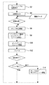
図3は、この発明の実施の形態1において、ダイボンディング装置により、ダイボンディングを行う場合の動作について説明するためのフロー図である。また、図4は、ウェハ30内のチップを処理する進捗状態を説明するための上面模式図である。
以下、図3、図4を参照して、ウェハ30のボンディング処理を行う手順について説明する。
FIG. 3 is a flowchart for explaining an operation when die bonding is performed by the die bonding apparatus in the first embodiment of the present invention. FIG. 4 is a schematic top view for explaining a progress state of processing chips in the
Hereinafter, a procedure for performing the bonding process of the
まず、ウェハテーブル2の第1エリアが処理範囲に位置するように、駆動手段16により、ウェハテーブル2を移動し、予め取得した中心チップ32aのデータに基づいて、位置合わせを行う(ステップS2)。その後、認識カメラ4により、第1エリアの対象チップ2の画像を認識する(ステップS4)。次に、対象チップ32の画像と、その対象チップ32に対応する、予め登録された位置合わせの基準となるテンプレート画像とを比較する。そして、制御手段18において、ピックアップユニット6の吸着部10及び突上ユニット8の中心に、対象チップ32の中心が重なるように、ウェハテーブル2の位置の補正量を算出する。駆動手段16は、この算出された補正量により、ウェハテーブル2を移動してウェハテーブル2の位置を決定する(ステップS6)。
First, the driving
次に、突上ユニット8により対象チップ32は突き上げられてウェハ30の粘着シートから剥離され、下方に移動したピックアップユニット6の吸着部10により吸着される(ステップS8)。そして、ピックアップユニット6により、リードフレーム34上の所定位置に移動され(ステップS10)、リードフレーム34にプレスされて(ステップS12)、対象チップ32の搭載が終了する。
Next, the
次に、第1エリア内に、まだ、ボンディングされていないチップ32が残っている場合には、次のチップ32を対象チップとして、上述したステップS4〜S12の方法により、ボンディングを行う。
Next, when the
第1エリア内の全てのチップのボンディングが終了したところで、ウェハテーブル2の回転を行う(ステップS14)。ここでは、ウェハテーブル2を、上面から見て左回りに90度回転する。この回転により、図4に示すように、第2エリアが、ウェハテーブル2の処理範囲に移動する。 When the bonding of all the chips in the first area is completed, the wafer table 2 is rotated (step S14). Here, the wafer table 2 is rotated 90 degrees counterclockwise as viewed from above. By this rotation, the second area moves to the processing range of the wafer table 2 as shown in FIG.
ここで、中心チップ32aの情報を基に、中心チップ32aの中心を回転軸とする。そして、マップがずれないように、中心チップ32aと回転中心で合成されるベクトルから、エリア回転時の中心チップ32a軌跡を算出し、回転後、再認識を実行し、中心チップ32aをサーチし、第2エリアの位置合わせを行う(ステップS2)。このとき、中心チップ32aが見つからない場合には、制御手段18は、X方向、Y方向に、それぞれ、1/2チップサイズ分ずつウェハテーブル2を移動して、中心チップ32aをサーチする。
Here, based on the information of the
その後、第2エリアについて、上述したステップS4〜S12を繰り返すことにより、第2エリアのチップ32のボンディングを行う。
但し、このとき、第2エリアのチップ32は、通常の状態から、左周りに90度回転した状態となっている。このため、ピックアップ動作(ステップS8)の際には、ピックアップユニット6は、その吸着部10を回転軸により、予め、左回りに90度回転させておく。そして、ピックアップ後、その移動の過程において(ステップS10)、回転させた吸着部10を元の位置に戻す。これにより、吸着部10及び保持されたチップ32は、右回りに90度回転し、チップ32は、ウェハステージ2の回転によるズレが修正され、通常の位置に戻された状態となる。この状態で、チップ32は、リードフレーム34にボンディングされる(ステップS12)。
Thereafter, the
However, at this time, the
第2エリア内の全ての対象チップのボンディングを行った後、再び、ウェハテーブル2を90度回転する(ステップS14)。この回転により、第3エリアがウェハテーブル2の処理範囲に移動し、第3エリア内のチップ32がボンディングの対象となる。その後、第3エリアについて、位置合わせ(ステップS2)を行い、第1エリア、第2エリアと同様にステップS4〜S12を繰り返すことによりチップ32のボンディングを行う。但し、第3エリアは、ウェハテーブル2を左回りに、合計で180度移動しているため、チップ32も、通常の状態から180度回転した状態となっている。従って、ピックアップ動作(ステップS8)の際には、ピックアップユニット6の吸着部10は、予め左周り、あるいは、右回りに180度回転させておいて、移動の過程において(ステップS10)、この180度の回転を元に戻す。
After bonding all the target chips in the second area, the wafer table 2 is again rotated by 90 degrees (step S14). By this rotation, the third area moves to the processing range of the wafer table 2, and the
第3エリアの全対象チップのボンディングが終了した後、ウェハテーブル2を、更に、左回りに90度回転する(ステップS14)。この回転により、第4エリアがウェハテーブル2の処理範囲に移動し、第4エリアのチップ32がボンディングの対象となる。再び、第4エリアについて、位置合わせ(ステップS2)を行い、ステップS4〜S12を繰り返すことにより、対象チップのボンディングを行う。ここで、第4エリアは、ステージを左回りに合計で270度回転しているため、第4エリアのチップは、通常の状態から、270度左回りに回転している。従って、吸着部10も、そのピックアップ動作時に、予め左回りに270度あるいは右回りに90度回転させておいて(ステップS8)、移動の過程において(ステップS10)、この回転を元に戻す。
After the bonding of all target chips in the third area is completed, the wafer table 2 is further rotated 90 degrees counterclockwise (step S14). By this rotation, the fourth area moves to the processing range of the wafer table 2, and the
以上のようにして、第1〜第4エリアの全チップ32のボンディングが終了した後、中心チップ32aのボンディングを行う。ここでは、第4エリアに続けて行うため、チップは、左回りに270度回転した状態にある。従って、第4エリアと同様に、吸着部10は、そのピックアップ動作時に、予め、左回りに270度あるいは右回りに90度回転させて、吸着させ(ステップS8)、移動時において(ステップS10)、その回転を元に戻した状態で、リードフレーム34にボンディングする。これにより、ウェハ30内の全てのチップ32についてのボンディングが終了する。
After the bonding of all the
以上説明したように、実施の形態1においては、ウェハ30内を4つのエリアに分割して、1のエリアのボンディングを行った後、次のエリアはウェハ30を90度回転させてボンディングを行う。従って、ウェハテーブル2の突上ユニット8に対するX、Y方向の移動範囲は、各エリアに対応した範囲、即ち、ウェハの概ね1/4程度の範囲でよく、例えば、8インチウェハを考えると、150mm×150mm程度の範囲でよい。従って、ウェハが大口径化する場合にも、ダイボンディング装置の小型化を図ることができる。また、ウェハテーブル2の移動範囲の大幅な拡大を必要としないため、従来の小さなウェハに対応する移動範囲しか持たないダイボンディング装置を改良するだけで、大口径化するウェハに対応することができる。
As described above, in the first embodiment, the inside of the
また、実施の形態1では、ピックアップユニット6によりチップをピックアップする際に、吸着部10を回転軸12により、予め、そのエリアの回転された角度にあわせて回転させておいて、リードフレーム34側に移動する際に、この回転を戻す。これにより、ウェハテーブル2の回転により方向の変ったチップ32を、移動において正常の向きに戻して、装着方向のズレを解消し、ボンディングすることができる。また、この回転は、ピックアップユニット6の移動時において行われるため、スループットを低下させることなく行うことができる。
In the first embodiment, when the
また、実施の形態1では、ウェハ30面内を4つのエリアに分割する際に、中心に、いずれのエリアにも属さない中心チップ32aを残し、この中心チップ32aの各辺の延長方向に沿って分割するように設定した。図2では、同形状のチップ32が、X、Y方向に奇数枚ずつ配置され、ウェハ30の中心に位置するチップを中心チップ32aとする場合について図示した。しかし、中心チップ32aとしては、ウェハ30の中心付近にあるチップを任意に選択することができる。
Further, in the first embodiment, when the
図5は、チップ32がX、Y方向にそれぞれ、偶数枚配置され、中心チップ32aの中心が、ウェハ30の中心と一致しない場合を表している。
例えば、図5に示すように、中心チップ32aが中心にない場合、例えば、チップが、X方向、Y方向にそれぞれ、偶数枚ずつ配置されているような場合であっても、中心付近にあるチップ32を中心チップ32aとして決め、これを基準とすることができる。そして、このチップ32aの中心を回転軸とする。また、チップの形状が異なっているようなものが複数個配置されている場合には、ウェハ30の中心に近いチップを中心チップ32aとすればよい。このように、実施の形態1は、ウェハ30に、奇数枚、偶数枚のチップが配置されているいずれの場合にも、また、形状の異なるチップが配置されている場合にも、適用することができる。
FIG. 5 shows a case where an even number of
For example, as shown in FIG. 5, when the
また、実施の形態1では、どのエリアにも属さない中心チップ32aを設けることにより、基準情報として、中心チップ32aの位置情報を登録する。そして、ウェハテーブル2回転の際には、このチップの位置を追尾、補正することで、ウェハ30のマップズレを防止することができる。
In the first embodiment, the position information of the
また、実施の形態1では、ウェハを4つに分割する場合について説明した。しかし、この発明はこれに限るものではなく、2つに分割するようなものであってもよい。但し、この場合、必要のウェハテーブル2の移動範囲が大きくなることを考慮する必要がある。ウェハ面内を半分のエリアに分割する場合には、例えば、ウェハを、180度回転させて、ボンディングを行うことができる。 In the first embodiment, the case where the wafer is divided into four has been described. However, the present invention is not limited to this, and may be divided into two. However, in this case, it is necessary to consider that the necessary movement range of the wafer table 2 becomes large. When the wafer surface is divided into half areas, for example, the wafer can be rotated 180 degrees for bonding.
また、実施の形態1では、ピックアップユニット6の吸着部10が予め、チップの位置のズレを補正する方向に回転させておく場合について説明した。しかし、この発明はこれに限るものではなく、例えば、ピックアップユニット6により吸着部10を吸着した後で、チップ32を回転させて、回転によるズレを戻すものであっても良い。
Further, in the first embodiment, the case where the
実施の形態2.
図6は、この発明の実施の形態2におけるウェハを説明するための上面図である。
実施の形態2におけるダイボンディング方法は、実施の形態1において説明したものと同様である。但し、実施の形態2においては、制御装置18により、各チップの位置合わせの際に用いるテンプレート画像を、各エリアごとに、基準画像から算出して登録する。
FIG. 6 is a top view for illustrating the wafer according to the second embodiment of the present invention.
The die bonding method in the second embodiment is the same as that described in the first embodiment. However, in the second embodiment, the
ここでは、まず、第1のエリアの基準画像となるチップの画像を認識カメラ4で取得して制御手段18に登録する。そして、制御手段18は、この第1エリアの基準画像を第1テンプレート画像として登録する。そして、その登録された第1テンプレート画像を、左回りに、90度、180度、270度左方向に画像処理で回転したものを作成し、これを、第2テンプレート画像、第3テンプレート画像、第4テンプレート画像として登録する。
Here, first, an image of a chip serving as a reference image of the first area is acquired by the
このとき、一般に、X方向、Y方向の認識カメラ4の分解能は異なっている。従って、この分解能の違いを補正するように、第1テンプレート画像は予め大きく取り込んでおく。そして、第1〜第4テンプレート画像作成においては、X方向Y方向の変換において不足するデータを補完するようにする。
At this time, generally, the resolutions of the
各エリアのチップ32をボンディングする際、対象チップの中心位置への移動の際の位置合わせにおいては(ステップS6)、このようにして作成した、第1〜第4テンプレート画像を、それぞれ、各エリアにおけるテンプレート画像として用いる。
When bonding the
以上説明したように、実施の形態2においては、第1のエリアから認識した1のチップ32の画像により、各エリアに対応するテンプレート画像を作成することができる。また、このテンプレート画像は、X方向、Y方向の分解能の違いを補完して作成する。従って、各エリアのチップ32に対するテンプレート画像の登録時間を削減して、各エリアに対応する正確なテンプレート画像を作成することができる。
As described above, in the second embodiment, a template image corresponding to each area can be created from the image of one
なお、実施の形態2においては、第1エリアから取得したテンプレート画像を基準として、これを回転させて、それぞれ第2〜第4エリアに対応するテンプレート画像を作成する場合について説明した。しかし、テンプレート画像の作成方法はこれに限るものではない。例えば、認識カメラ4を、ウェハテーブル2の回転角度にあわせて回転させて、各チップ32の画像を取得することにより、テンプレート画像を1画像としたものであってもよい。
In the second embodiment, a case has been described in which template images acquired from the first area are rotated with reference to the template images corresponding to the second to fourth areas. However, the template image creation method is not limited to this. For example, the
実施の形態3.
図7は、この発明の実施の形態3におけるウェハ30を説明するための上面図である。また、図8は、この発明の実施の形態3において、ウェハ30からピックアップしたチップを積層する場合の状態を説明するための模式図である。
FIG. 7 is a top view for illustrating a
実施の形態2において説明した方法は、ウェハ30内に同一パターンのチップが形成されている場合に有効である。これに対して、実施の形態3では、ウェハ内の第1〜第4エリアに、それぞれ、異なるパターンのチップが形成された場合について説明する。
The method described in the second embodiment is effective when chips having the same pattern are formed in the
実施の形態3においては、第1エリアにおいては、中心チップ32aによりエリアの位置合わせを行った後(ステップS2)、ボンディングの開始前に、任意のチップ32の画像を、テンプレート画像として読み込んで、テンプレート画像として登録する。そして、各チップ32のボンディング処理においては、このテンプレート画像を位置合わせに用いる。同様に、第2〜第4エリアのテンプレート画像は、ウェハテーブル2が回転する際の、中心チップ32aの回転軌跡の計算結果を基にして、回転後の位置合わせを行った後、認識カメラ4により処理範囲にあるエリアの、任意のチップの画像をテンプレート画像として登録する。そして、各エリアについても、これをテンプレート画像として登録して、位置合わせに用いる。
In the third embodiment, in the first area, after the area is aligned by the
このようにすることにより、例えば、ウェハ30面内の各エリアごとに、異なるパターンのチップが形成されている場合にも、チップ32の位置合わせ用のテンプレート画像を準備する時間を抑えることができる。また、各エリアごとに、異なるパターンのチップ32を形成すれば、例えば、ウェハ30を取り替えることなく、図9に示すように、複数の異なるチップを、リードフレーム34に積層することができる。このようにして、ウェハ30取替えの時間を省略することもできる。
By doing so, for example, even when chips with different patterns are formed for each area in the surface of the
なお、実施の形態3においては、各エリアごとに、回転後にテンプレート画像を取得する場合について説明した。しかし、この発明はこれに限るものではない。テンプレート画像は、各パターンごとに、また、各エリアの回転角度毎に必要となる。従って、例えば、第1〜第4エリアにおいて、同じパターンのチップと、異なるパターンのチップが混在している場合には、実施の形態2、3において説明した方法を組み合わせて、同じパターンのチップについては、各エリアごとに、第1エリアにおいて取得した基準画像を回転させることでテンプレート画像を作成し、異なるパターンについては、そのチップが含まれるエリアで取得した画像をテンプレート画像として用いればよい。また、実施の形態2において説明したように、認識カメラ4を、ウェハ30の回転角度にあわせて回転させたものであってもよい。
In the third embodiment, the case where a template image is acquired after rotation has been described for each area. However, the present invention is not limited to this. A template image is required for each pattern and for each rotation angle of each area. Therefore, for example, in the first to fourth areas, when chips with the same pattern and chips with different patterns are mixed, the methods described in the second and third embodiments are combined to obtain chips with the same pattern. For each area, a template image is created by rotating the reference image acquired in the first area. For different patterns, the image acquired in the area including the chip may be used as the template image. Further, as described in the second embodiment, the
実施の形態4.
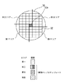
図9は、この発明の実施の形態4におけるボンディング方法における、不良チップの特定方法について説明するための模式図である。
例えば、半導体チップに不良が発生している場合に、不良識別マークが用いられず、ウェハのIDなどをキー情報として、ウェハの良品/不良マップで処理する場合がある(以下、「マップデータ」と称する)。実施の形態4では、このようなマップデータを、認識する方法について説明する。
FIG. 9 is a schematic diagram for explaining a defective chip identifying method in the bonding method according to the fourth embodiment of the present invention.
For example, when a defect occurs in a semiconductor chip, a defect identification mark is not used, and processing may be performed on a non-defective / defective map of the wafer using the wafer ID as key information (hereinafter referred to as “map data”). Called). In the fourth embodiment, a method for recognizing such map data will be described.
ここでは、中心チップ32aを基準として用いる。そして、まず、図9の矢印(1)〜(4)に示すように、初期データとして、第1〜第4エリアのそれぞれについて、中心チップ32aからのチップ数をカウントする。そして、このカウントしたチップ数を基にして、ウェハ全体の基点を求めて、制御手段18に登録する。
制御手段18は、この基点を中心にして、ウェハとマップデータを重ね合わせて、各エリアごとに不良チップを特定しながら、処理を行う。
Here, the
The control means 18 performs processing while superimposing the wafer and map data around this base point and specifying defective chips for each area.
以上のようにして、視野の限られた1/4エリアずつの処理においても、マップデータを投入することができる。
また特徴的なターゲットを予め準備させておいて、このパターンを認識させることによりマップデータとウェハとを重ね合わせるものとしてもよい。また、予め登録された中心チップ32aをウェハの基点と求めるために用いることも考えられる。
As described above, map data can be input even in the processing of each 1/4 area with a limited field of view.
Further, a characteristic target may be prepared in advance, and the map data and the wafer may be overlapped by recognizing this pattern. It is also conceivable to use the
なお、実施の形態1〜4においては、全てダイボンディング装置について説明したが、この発明はこれに限るものではなく、例えば、FCB(フリップチップボンダ)など、ウェハからチップをピックアップする機能を有する他の装置に適用することができる。 In the first to fourth embodiments, the die bonding apparatus has been described. However, the present invention is not limited to this. For example, an FCB (flip chip bonder) or the like has a function of picking up a chip from a wafer. It can be applied to other devices.
なお、例えば、実施の形態1〜4において、ダイボンディング装置は、この発明の「実装装置」に該当し、実施の形態1〜4における、ウェハテーブル2、突上ユニット8、ピックアップユニット6は、それぞれ、この発明の「ウェハテーブル」、「突上部」、「保持部」に該当する。また、例えば、実施の形態1〜4における、駆動手段16は、この発明の「駆動機構」及び「テーブル回転機構」に該当し、回転軸12は、「保持部回転機構」に該当する。また、例えば、実施の形態1〜4における、認識カメラ4、制御手段18は、それぞれ、この発明の「認識カメラ」、「制御手段」に該当する。また、例えば、リードフレーム34は、この発明の「基板」に該当する。
For example, in the first to fourth embodiments, the die bonding apparatus corresponds to the “mounting apparatus” of the present invention. In the first to fourth embodiments, the wafer table 2, the
2 ウェハテーブル
4 認識カメラ
6 ピックアップユニット
8 突上ユニット
10 吸引部
12 回転軸
14 回転軸
16 駆動手段
18 制御手段
20 リードフレーム台
30 ウェハ
32 チップ
32a 中心チップ
34 リードフレーム
2 Wafer Table 4
Claims (9)
前記ウェハを載置するウェハテーブルと、
前記ウェハテーブルに載置された前記ウェハ内の複数のチップのいずれかを押し上げる突上部と、
前記突上部に押し上げられたチップを保持して、前記基板上に移動する保持部と、
を備え、
前記ウェハテーブルは、
前記ウェハ内の複数のチップのうち、装着の対象となるチップが、前記突上部上方に位置するように、所定の移動範囲内で、前記ウェハを移動させる駆動機構と、
前記ウェハ面内を、前記ウェハの中心付近にあるチップを中心チップとして、前記中心チップの4辺を、それぞれ一方向に、かつ、対向する2辺については互いに別の方向に、延びるように延長させた延長線により4つのエリアに分けた場合に、前記エリアのうちいずれか1のエリアが、前記ウェハテーブルの前記所定の移動範囲内に位置するように、前記ウェハテーブルを基準位置から所定の角度回転させるテーブル回転機構と、
を備えることを特徴とする実装装置。 A mounting apparatus for holding a chip divided into a plurality of pieces in a wafer and mounting the chip on a substrate,
A wafer table for mounting the wafer;
A protrusion that pushes up any of a plurality of chips in the wafer placed on the wafer table;
A holding unit that holds the chip pushed up on the protruding portion and moves onto the substrate;
With
The wafer table is
A drive mechanism for moving the wafer within a predetermined movement range so that a chip to be mounted among the plurality of chips in the wafer is positioned above the protrusion;
Within the wafer surface, a chip near the center of the wafer is used as a central chip, and the four sides of the central chip are extended in one direction and two opposing sides in different directions. When the extended line is divided into four areas, the wafer table is moved from a reference position to a predetermined position so that any one of the areas is located within the predetermined movement range of the wafer table. A table rotation mechanism for rotating the angle;
A mounting apparatus comprising:
前記ウェハテーブルの前記所定の移動範囲内にある前記エリアの画像を認識できる認識カメラと、
前記認識カメラにより認識された前記エリアの画像から、基準となるチップの画像を基準画像として登録し、前記4つのエリアのそれぞれに対する前記ウェハテーブルの回転角度に応じて、前記基準画像を、それぞれ、0度、90度、180度、270度に回転させた画像を、前記各エリアに対応するテンプレート画像として登録し、
前記認識カメラにより認識された前記エリアの画像と、前記登録された前記エリアに対応するテンプレート画像とを比較して、前記ウェハテーブルを所定の位置に移動して、位置合わせを行う制御部と、
を備えることを特徴とする請求項1又は2に記載の実装装置。 The mounting apparatus is:
A recognition camera capable of recognizing an image of the area within the predetermined movement range of the wafer table;
From the image of the area recognized by the recognition camera, a reference chip image is registered as a reference image, and the reference image is set according to the rotation angle of the wafer table with respect to each of the four areas. Register images rotated at 0 degrees, 90 degrees, 180 degrees, and 270 degrees as template images corresponding to the areas,
A controller that compares the image of the area recognized by the recognition camera with a template image corresponding to the registered area, moves the wafer table to a predetermined position, and performs alignment;
The mounting apparatus according to claim 1, further comprising:
前記ウェハテーブルの前記所定の移動範囲内にある前記エリアの画像を認識できる認識カメラと、
前記認識カメラにより認識された前記4つのエリアの各画像から、それぞれ1つずつ、基準となるチップを選択し、前記各チップの画像を、前記各エリアに対応するテンプレート画像として登録し、
前記認識カメラにより認識された画像と、前記予め登録された前記各エリアに対応するテンプレート画像とを比較して、前記ウェハテーブルを所定の位置に移動する制御部と、
を備えることを特徴とする請求項1又は2に記載の実装装置。 The mounting apparatus is:
A recognition camera capable of recognizing an image of the area within the predetermined movement range of the wafer table;
From each image of the four areas recognized by the recognition camera, select one chip as a reference, register the image of each chip as a template image corresponding to each area,
A controller that compares the image recognized by the recognition camera with a template image corresponding to each of the previously registered areas, and moves the wafer table to a predetermined position;
The mounting apparatus according to claim 1, further comprising:
前記ウェハテーブルの移動範囲内にある前記エリアの画像を認識できる認識カメラと、
前記ウェハテーブルを所定の位置に移動する制御部と、
を備え、
前記制御部は、前記ウェハ中の前記チップ中の不良チップを特定する、前記ウェハ全面に関するデータマップを有し、
前記ウェハの各エリアの、前記中心チップからのチップの数を登録し、前記データマップの前記中心チップに対応する位置を、前記登録されたチップ数から割り出して、前記認識カメラにより認識された画像と、前記データマップとを重ねて、不良チップの位置を特定することを特徴とする請求項1〜4のいずれかに記載の実装装置。 The mounting apparatus is:
A recognition camera capable of recognizing an image of the area within the movement range of the wafer table;
A control unit for moving the wafer table to a predetermined position;
With
The control unit has a data map for identifying the defective chip in the chip in the wafer, the data map relating to the entire surface of the wafer,
The number of chips from the central chip in each area of the wafer is registered, and the position corresponding to the central chip in the data map is calculated from the registered number of chips, and the image recognized by the recognition camera. The mounting apparatus according to claim 1, wherein a position of a defective chip is specified by superimposing the data map.
前記ウェハの中心付近の1のチップを中心チップとして選択し、
前記中心チップの4辺を、それぞれ一方向に、かつ、対向する2辺については互いに別の方向に、延びるように延長させた延長線により、前記ウェハ面内を、前記中心チップに接する中心角が90度である第1、第2、第3、第4エリアに分割し、
前記第1エリアが、前記ウェハテーブルの所定の移動範囲内に配置されるようにして、前記1エリア内の前記チップを、それぞれ、前記保持部により前記基板に装着した後、
前記ウェハテーブルを90度回転させて前記第2エリアが前記所定の移動範囲内に配置されるようにし、前記第2エリア内の前記各チップを、前記保持部により保持した状態で前記ウェハテーブルの回転と逆の方向に90度回転させて、前記基板に装着し、
前記ウェハテーブルを90度回転させて、前記第3エリアが前記所定の移動範囲内に配置されるようにし、前記第3エリア内の前記各チップを、前記保持部により保持した状態で前記ウェハテーブルの回転と逆の方向に180度回転させて、前記基板に装着し、
前記ウェハテーブルを90度回転させて、前記第4エリアが前記所定の移動範囲内に配置されるようにし、前記第4エリア内の前記各チップを、前記保持部により保持した状態で前記ウェハテーブルの回転と逆の方向に270度回転させ、前記基板に装着し、
前記中心チップを、前記保持部により保持した状態で前記ウェハテーブルの回転と逆の方向に270度回転させ、前記保持部により前記基板に装着する、
ことを特徴とする実装方法。 In a mounting method in which a wafer on which a plurality of chips are formed is placed on a wafer table, one chip is picked up by a holding unit, and mounted on a substrate.
Select one chip near the center of the wafer as the center chip,
A central angle in contact with the central chip in the wafer surface by extension lines extending so that the four sides of the central chip extend in one direction and in two directions opposite to each other. Is divided into first, second, third, and fourth areas that are 90 degrees,
After the first area is disposed within a predetermined movement range of the wafer table and the chips in the one area are respectively mounted on the substrate by the holding unit,
The wafer table is rotated by 90 degrees so that the second area is disposed within the predetermined movement range, and the chips in the second area are held by the holding unit while being held by the holding unit. Rotate 90 degrees in the opposite direction of rotation, and attach it to the board,
The wafer table is rotated by 90 degrees so that the third area is disposed within the predetermined movement range, and the chips in the third area are held by the holding unit. Rotate 180 degrees in the opposite direction to the rotation of
The wafer table is rotated 90 degrees so that the fourth area is disposed within the predetermined movement range, and the chips in the fourth area are held by the holding unit while being held by the holding unit. 270 degrees in the opposite direction to the rotation of, and attached to the substrate,
The center chip is rotated by 270 degrees in the direction opposite to the rotation of the wafer table while being held by the holding unit, and is mounted on the substrate by the holding unit.
An implementation method characterized by that.
前記取得された画像から、基準となるチップの画像を第1テンプレート画像として登録し、
前記第1テンプレート画像を、それぞれ、90度、180度、270度に回転させた画像を、それぞれ、第2、第3、第4テンプレート画像として登録し、
前記第1エリア内の装着対象となるチップごとに、前記1エリアの画像と、前記第1テンプレート画像とを比較して、前記ウェハテーブルを移動して位置合わせを行った後、前記装着対象のチップの装着を行い、
前記第2エリアの前記チップ装着前に、前記認識カメラにより、前記第2エリアの画像を取得し、
前記第2エリア内の装着対象となるチップごとに、前記2エリアの画像と、前記第2テンプレート画像とを比較して、前記ウェハテーブルを移動して位置合わせを行った後、前記装着対象のチップの装着を行い、
前記第3エリアのチップ装着前に、前記認識カメラにより、前記第3エリアの画像を取得し、
前記第3エリア内の装着対象となるチップごとに、前記第3エリアの画像と、前記第3テンプレート画像とを比較して、前記ウェハテーブルを移動して位置合わせを行った後、前記装着対象のチップの装着を行い、
前記第4エリアのチップ装着前に、前記認識カメラにより、前記第4エリアの画像を取得し、
前記第4エリア内の装着対象となるチップごとに、前記第4エリアの画像と、前記第4テンプレート画像とを比較して、前記ウェハテーブルを移動して位置合わせを行った後、前記装着対象のチップの装着を行うことを特徴とする請求項6に記載の実装方法。 Before attaching the chip in the first area, an image of the first area is acquired by a recognition camera,
From the acquired image, a reference chip image is registered as a first template image,
Images obtained by rotating the first template image by 90 degrees, 180 degrees, and 270 degrees, respectively, are registered as second, third, and fourth template images, respectively.
For each chip to be mounted in the first area, the image of the one area is compared with the first template image, and the wafer table is moved and aligned. Insert the tip,
Before attaching the chip in the second area, the recognition camera acquires an image of the second area,
For each chip to be mounted in the second area, the image of the two areas is compared with the second template image, the wafer table is moved and aligned, and then the mounting target Insert the tip,
Before attaching the chip of the third area, the recognition camera acquires an image of the third area,
For each chip to be mounted in the third area, the image of the third area is compared with the third template image, the wafer table is moved and aligned, and then the mounting target Of the tip,
Before attaching the chip in the fourth area, the recognition camera acquires an image of the fourth area,
For each chip to be mounted in the fourth area, the image of the fourth area is compared with the fourth template image, the wafer table is moved and aligned, and then the mounting target The mounting method according to claim 6, wherein the chip is mounted.
前記第1エリアの画像から、基準となるチップの画像を第1テンプレート画像として登録し、
前記第1エリアの装着対象となるチップごとに、前記第1テンプレート画像と、前記第1エリアの画像とを比較して、前記ウェハテーブルを移動して位置合わせを行った後、前記装着対象のチップの装着を行い、
前記第2エリアのチップ装着前に、前記認識カメラにより、前記第2エリアの画像を取得し、
前記第2エリアの画像から、基準となるチップの画像を第2テンプレート画像として登録し、
前記第2エリアの装着対象となるチップごとに、前記第2テンプレート画像と、前記第2エリアの画像とを比較して、前記ウェハテーブルを移動して位置合わせを行った後、前記装着対象のチップの装着を行い、
前記第3エリアのチップ装着前に、前記認識カメラにより、前記第3エリアの画像を取得し、
前記第3エリアの画像から、基準となるチップの画像を第3テンプレート画像として登録し、
前記第3エリアの装着対象となるチップごとに、前記第3テンプレート画像と、前記第3エリアの画像とを比較して、前記ウェハテーブルを移動して位置合わせを行った後、前記装着対象のチップの装着を行い、
前記第4エリアのチップ装着前に、前記認識カメラにより、前記第4エリアの画像を取得し、
前記第4エリアの画像から、基準となるチップの画像を第4テンプレート画像として登録し、
前記第4エリアの装着対象となるチップごとに、前記第4テンプレート画像と、前記第4エリアの画像とを比較して、前記ウェハテーブルを移動して位置合わせを行った後、前記装着対象のチップの装着を行うことを特徴とする請求項6に記載の実装方法。 Before attaching the chip in the first area, an image of the first area is acquired by a recognition camera,
From the image of the first area, register a reference chip image as a first template image,
For each chip to be mounted in the first area, the first template image and the image in the first area are compared, and the wafer table is moved and aligned. Insert the tip,
Before attaching the second area chip, the recognition camera acquires an image of the second area,
From the image of the second area, register a reference chip image as a second template image,
For each chip to be mounted in the second area, the second template image and the image in the second area are compared, and after the wafer table is moved and aligned, the mounting target Insert the tip,
Before attaching the chip of the third area, the recognition camera acquires an image of the third area,
From the image of the third area, register a reference chip image as a third template image,
For each chip to be mounted in the third area, the third template image is compared with the image in the third area, the wafer table is moved and aligned, and then the mounting target Insert the tip,
Before attaching the chip in the fourth area, the recognition camera acquires an image of the fourth area,
From the image of the fourth area, register the image of the reference chip as a fourth template image,
For each chip to be mounted in the fourth area, the fourth template image is compared with the image in the fourth area, and after the wafer table is moved and aligned, the mounting target The mounting method according to claim 6, wherein a chip is mounted.
前記ウェハの、前記中心チップからの前記チップの数を前記エリアごとに数えて、前記各エリアの前記チップ数を登録し、
前記ウェハ内のチップ中の不良チップを特定する、ウェハ全面に関するデータマップの、前記中心チップに対応する位置を、前記登録されたチップ数から割り出して、
前記各エリアの画像と、前記データマップとを重ねて、前記不良チップを特定することを特徴とする請求項6〜8のいずれかに記載の実装方法。
The image of each area is acquired by a recognition camera,
Count the number of chips from the central chip of the wafer for each area, and register the number of chips in each area,
The position corresponding to the central chip of the data map relating to the entire wafer surface that identifies a defective chip among the chips in the wafer is determined from the number of registered chips,
The mounting method according to claim 6, wherein the defective chip is specified by overlapping the image of each area and the data map.
Priority Applications (1)
| Application Number | Priority Date | Filing Date | Title |
|---|---|---|---|
| JP2004320748A JP2006135013A (en) | 2004-11-04 | 2004-11-04 | Mounting device and mounting method |
Applications Claiming Priority (1)
| Application Number | Priority Date | Filing Date | Title |
|---|---|---|---|
| JP2004320748A JP2006135013A (en) | 2004-11-04 | 2004-11-04 | Mounting device and mounting method |
Publications (2)
| Publication Number | Publication Date |
|---|---|
| JP2006135013A true JP2006135013A (en) | 2006-05-25 |
| JP2006135013A5 JP2006135013A5 (en) | 2007-12-20 |
Family
ID=36728301
Family Applications (1)
| Application Number | Title | Priority Date | Filing Date |
|---|---|---|---|
| JP2004320748A Pending JP2006135013A (en) | 2004-11-04 | 2004-11-04 | Mounting device and mounting method |
Country Status (1)
| Country | Link |
|---|---|
| JP (1) | JP2006135013A (en) |
Cited By (7)
| Publication number | Priority date | Publication date | Assignee | Title |
|---|---|---|---|---|
| JP2012175037A (en) * | 2011-02-24 | 2012-09-10 | Hitachi High-Tech Instruments Co Ltd | Die bonder and semiconductor manufacturing method |
| KR20130029707A (en) * | 2011-09-15 | 2013-03-25 | 가부시끼가이샤 히다찌 하이테크 인스트루먼츠 | Die bonder and bonding method |
| JP2017092315A (en) * | 2015-11-12 | 2017-05-25 | 富士機械製造株式会社 | Electronic component mounting machine |
| KR20170121909A (en) * | 2016-04-26 | 2017-11-03 | 세메스 주식회사 | Apparatus and method for bonding dies onto wafer |
| DE102016116345A1 (en) | 2016-09-01 | 2018-03-01 | Infineon Technologies Ag | METHOD FOR ASSEMBLING SEMICONDUCTOR COMPONENTS |
| CN109638142A (en) * | 2019-01-22 | 2019-04-16 | 先进光电器材(深圳)有限公司 | Brilliant loop device |
| CN115831815A (en) * | 2022-11-23 | 2023-03-21 | 中科长光精拓智能装备(苏州)有限公司 | Chip mounting system and mounting method thereof |
Citations (6)
| Publication number | Priority date | Publication date | Assignee | Title |
|---|---|---|---|---|
| JPS6057942A (en) * | 1983-09-09 | 1985-04-03 | Toshiba Corp | Mounting device for pellet |
| JPS62295431A (en) * | 1986-06-13 | 1987-12-22 | Nichiden Mach Ltd | Work pickup apparatus |
| JPH03294976A (en) * | 1990-04-13 | 1991-12-26 | Matsushita Electric Ind Co Ltd | Reference mark pattern detecting device |
| JPH0722475A (en) * | 1993-06-29 | 1995-01-24 | Oki Electric Ind Co Ltd | Die bonding method and die bonder |
| JP2001196444A (en) * | 1999-08-27 | 2001-07-19 | Matsushita Electric Ind Co Ltd | Method and apparatus for handling aligned components |
| JP2004055645A (en) * | 2002-07-17 | 2004-02-19 | Hitachi High-Tech Instruments Co Ltd | System and method for picking up die |
-
2004
- 2004-11-04 JP JP2004320748A patent/JP2006135013A/en active Pending
Patent Citations (6)
| Publication number | Priority date | Publication date | Assignee | Title |
|---|---|---|---|---|
| JPS6057942A (en) * | 1983-09-09 | 1985-04-03 | Toshiba Corp | Mounting device for pellet |
| JPS62295431A (en) * | 1986-06-13 | 1987-12-22 | Nichiden Mach Ltd | Work pickup apparatus |
| JPH03294976A (en) * | 1990-04-13 | 1991-12-26 | Matsushita Electric Ind Co Ltd | Reference mark pattern detecting device |
| JPH0722475A (en) * | 1993-06-29 | 1995-01-24 | Oki Electric Ind Co Ltd | Die bonding method and die bonder |
| JP2001196444A (en) * | 1999-08-27 | 2001-07-19 | Matsushita Electric Ind Co Ltd | Method and apparatus for handling aligned components |
| JP2004055645A (en) * | 2002-07-17 | 2004-02-19 | Hitachi High-Tech Instruments Co Ltd | System and method for picking up die |
Cited By (13)
| Publication number | Priority date | Publication date | Assignee | Title |
|---|---|---|---|---|
| JP2012175037A (en) * | 2011-02-24 | 2012-09-10 | Hitachi High-Tech Instruments Co Ltd | Die bonder and semiconductor manufacturing method |
| TWI608556B (en) * | 2011-09-15 | 2017-12-11 | 捷進科技有限公司 | Die bonder and bonding method |
| KR20130029707A (en) * | 2011-09-15 | 2013-03-25 | 가부시끼가이샤 히다찌 하이테크 인스트루먼츠 | Die bonder and bonding method |
| JP2013065627A (en) * | 2011-09-15 | 2013-04-11 | Hitachi High-Tech Instruments Co Ltd | Die bonder and bonding method |
| KR101977987B1 (en) * | 2011-09-15 | 2019-05-13 | 파스포드 테크놀로지 주식회사 | Die bonder and bonding method |
| CN107359131A (en) * | 2011-09-15 | 2017-11-17 | 捷进科技有限公司 | Chip engagement machine and joint method |
| JP2017092315A (en) * | 2015-11-12 | 2017-05-25 | 富士機械製造株式会社 | Electronic component mounting machine |
| KR20170121909A (en) * | 2016-04-26 | 2017-11-03 | 세메스 주식회사 | Apparatus and method for bonding dies onto wafer |
| KR102580580B1 (en) | 2016-04-26 | 2023-09-20 | 세메스 주식회사 | Apparatus and method for bonding dies onto wafer |
| DE102016116345A1 (en) | 2016-09-01 | 2018-03-01 | Infineon Technologies Ag | METHOD FOR ASSEMBLING SEMICONDUCTOR COMPONENTS |
| DE102016116345B4 (en) * | 2016-09-01 | 2018-05-09 | Infineon Technologies Ag | METHOD FOR ASSEMBLING SEMICONDUCTOR COMPONENTS |
| CN109638142A (en) * | 2019-01-22 | 2019-04-16 | 先进光电器材(深圳)有限公司 | Brilliant loop device |
| CN115831815A (en) * | 2022-11-23 | 2023-03-21 | 中科长光精拓智能装备(苏州)有限公司 | Chip mounting system and mounting method thereof |
Similar Documents
| Publication | Publication Date | Title |
|---|---|---|
| JP6510838B2 (en) | Bonding apparatus and bonding method | |
| KR102132094B1 (en) | Electronic component mounting device and electronic component mounting method | |
| US11295996B2 (en) | Systems and methods for bonding semiconductor elements | |
| US10694651B2 (en) | Chip-placing method performing an image alignment for chip placement and chip-placing apparatus thereof | |
| JP7208732B2 (en) | Alignment method | |
| US20210020483A1 (en) | Die pickup method | |
| JP2006135013A (en) | Mounting device and mounting method | |
| JP4122170B2 (en) | Component mounting method and component mounting apparatus | |
| JP4314021B2 (en) | Wafer center detection method, and semiconductor chip pickup method and apparatus | |
| JP5690535B2 (en) | Die bonder and semiconductor manufacturing method | |
| JP2009054964A (en) | Wafer transfer apparatus, and semiconductor manufacturing apparatus equipped with the same | |
| JP2002198415A (en) | Apparatus and method of wafer alignment | |
| JP4262171B2 (en) | Semiconductor chip mounting apparatus and mounting method | |
| JP2006041006A (en) | Bonding method and apparatus for semiconductor chip | |
| JP2019121721A (en) | Electronic component mounting device and mounting method | |
| JP4761672B2 (en) | Bonding method and bonding apparatus | |
| JP3763229B2 (en) | Position detection method by image recognition | |
| JP2010212527A (en) | Bonding method and bonding device | |
| JP5181383B2 (en) | Bonding equipment | |
| JP2000277991A (en) | Apparatus and method for mounting component | |
| JP2010192817A (en) | Pickup method and pickup device | |
| TWI841852B (en) | Mounting device and mounting method | |
| JP2018006510A (en) | Component mounting device | |
| JP2019054027A (en) | Position specification method and position specification device and component mounting device | |
| JP2006253384A (en) | Bonding equipment and method for manufacturing semiconductor device |
Legal Events
| Date | Code | Title | Description |
|---|---|---|---|
| A521 | Written amendment |
Free format text: JAPANESE INTERMEDIATE CODE: A523 Effective date: 20071101 |
|
| A621 | Written request for application examination |
Free format text: JAPANESE INTERMEDIATE CODE: A621 Effective date: 20071101 |
|
| A977 | Report on retrieval |
Free format text: JAPANESE INTERMEDIATE CODE: A971007 Effective date: 20080331 |
|
| A711 | Notification of change in applicant |
Effective date: 20100521 Free format text: JAPANESE INTERMEDIATE CODE: A712 |
|
| A131 | Notification of reasons for refusal |
Effective date: 20100824 Free format text: JAPANESE INTERMEDIATE CODE: A131 |
|
| A02 | Decision of refusal |
Effective date: 20101221 Free format text: JAPANESE INTERMEDIATE CODE: A02 |