JP2006114747A - Method for manufacturing semiconductor device - Google Patents
Method for manufacturing semiconductor device Download PDFInfo
- Publication number
- JP2006114747A JP2006114747A JP2004301462A JP2004301462A JP2006114747A JP 2006114747 A JP2006114747 A JP 2006114747A JP 2004301462 A JP2004301462 A JP 2004301462A JP 2004301462 A JP2004301462 A JP 2004301462A JP 2006114747 A JP2006114747 A JP 2006114747A
- Authority
- JP
- Japan
- Prior art keywords
- film
- fluorine
- semiconductor device
- high dielectric
- manufacturing
- Prior art date
- Legal status (The legal status is an assumption and is not a legal conclusion. Google has not performed a legal analysis and makes no representation as to the accuracy of the status listed.)
- Withdrawn
Links
Images


Abstract
Description
本発明は、半導体装置の製造方法に関するもので、詳しくは、絶縁ゲート電界効果トランジスタ(MISFET)用のゲート絶縁膜に高誘電率膜(High−k膜)が適用される半導体装置の製造方法に関する。 The present invention relates to a method for manufacturing a semiconductor device, and more particularly to a method for manufacturing a semiconductor device in which a high dielectric constant film (High-k film) is applied to a gate insulating film for an insulated gate field effect transistor (MISFET). .
シリコン基板上に絶縁膜とゲート電極を形成した半導体装置において、絶縁膜にフッ素を添加することにより、シリコン基板との界面に存在するダングリングボンドを終端させることは、特許文献1に示されているが、電極形成前に低温でフッ素アニール処理を行う点が示されていない。
メタルゲートは、通常、high−k膜に有利な材料であるが、high−k膜の成膜温度は、低い場合が多く、シリコン基板界面状態を良好にする熱工程を経ていないのが普通である。また、先にシリコン基板中にソースドレインを形成する工程(ダマシンゲートなどゲート後付けプロセス)では、サリサイドの形成(例えばNiSiでは500℃未満)を行った後に、本来の絶縁膜を形成する場合が多く、これも高温化を適用できない一つの要因となっている。 A metal gate is usually a material advantageous for a high-k film, but the film-forming temperature of a high-k film is often low, and it is normal that it does not go through a thermal process that improves the silicon substrate interface state. is there. Further, in the process of forming the source / drain in the silicon substrate (gate retrofitting process such as damascene gate), the original insulating film is often formed after the salicide is formed (for example, less than 500 ° C. for NiSi). This is another factor that cannot be applied at high temperatures.
このように、低温化に伴い、シリコン基板の界面の状態が熱工程で回復せず、界面準位が多いことが避けて通れない。これを低減する方法として、水素アニール工程を行うことが挙げられるが、水素や重水素ではその回復の度合いが温度で制限されてしまい、例えば配線形成後に行うシンターリング工程では約500℃未満で、大きな効果が期待できない。 As described above, it is inevitable that the interface state of the silicon substrate is not recovered by the thermal process as the temperature is lowered, and there are many interface states. As a method for reducing this, it is possible to perform a hydrogen annealing step. However, in hydrogen and deuterium, the degree of recovery is limited by temperature. For example, a sintering step performed after wiring formation is less than about 500 ° C., A big effect cannot be expected.
また、水素は界面付近に存在する場合、NBTI(Negative Bias Temperature Instability)をより悪化させると言われており、信頼性に対する影響が大きい。また、イオン注入でフッ素を導入する方法については、例えばゲート後付け工程(ダマシンゲートプロセスなど)を経る場合、十分に界面にフッ素を導入することが困難である。 Further, when hydrogen is present in the vicinity of the interface, it is said that NBTI (Negative Bias Temperature Instability) is further deteriorated, which greatly affects reliability. As for the method of introducing fluorine by ion implantation, it is difficult to sufficiently introduce fluorine to the interface when, for example, a gate post-attachment process (damascene gate process or the like) is performed.
以上のように、シリコン基板の界面の改質に必要な高温化の導入不可能、シンターの限界があることから、デバイスへ与える影響は計り知れないものがある。界面準位の増加に伴い、例えば移動度の劣化、BTストレス耐性の低減など、深刻な問題が存在する。 As described above, it is impossible to introduce the high temperature required for the modification of the interface of the silicon substrate, and there is a limit of the sinter, so the influence on the device is immeasurable. As the interface state increases, there are serious problems such as deterioration of mobility and reduction of resistance to BT stress.
本発明は、上述の事情に鑑みてなされたもので、MISFETにおいてhigh−k膜を含むゲート絶縁膜(高誘電体ゲート絶縁膜)にフッ素を低温下で導入し、高性能なMISFETを可能にする半導体装置の製造方法を提供することを目的とする。 The present invention has been made in view of the above-described circumstances. In a MISFET, fluorine is introduced into a gate insulating film (high dielectric gate insulating film) including a high-k film at a low temperature, thereby enabling a high-performance MISFET. An object of the present invention is to provide a method for manufacturing a semiconductor device.
上記課題を解決するために、半導体装置の製造方法にかかる第1の発明は、シリコン基板上にhigh−k膜とゲート電極を形成する半導体装置の製造方法において、high−k膜形成後にフッ素雰囲気でアニール処理を施し、その後のプロセス温度を600℃以下、500℃程度で行うという構成を有している。 In order to solve the above problems, a first invention according to a method for manufacturing a semiconductor device is a method for manufacturing a semiconductor device in which a high-k film and a gate electrode are formed on a silicon substrate. An annealing process is performed, and the subsequent process temperature is 600 ° C. or lower and about 500 ° C.
そして、半導体装置の製造方法にかかる第2の発明は、シリコン基板上にhigh−k膜とゲート電極を形成する半導体装置の製造方法において、high−k膜形成後にhigh−k膜に積層した極薄絶縁膜を形成し、上記high−k膜と極薄絶縁膜の界面領域にフッ素を含有させるという構成を有している。 According to a second aspect of the present invention, there is provided a method for manufacturing a semiconductor device in which a high-k film and a gate electrode are formed on a silicon substrate, wherein the electrode is stacked on the high-k film after the high-k film is formed. A thin insulating film is formed, and fluorine is contained in the interface region between the high-k film and the ultrathin insulating film.
本発明は、シリコン基板と高誘電体ゲート絶縁膜の界面および高誘電体ゲート絶縁膜の膜質を改質して、MISFETの特性の向上を図ることができる。 The present invention can improve the characteristics of the MISFET by modifying the interface between the silicon substrate and the high dielectric gate insulating film and the film quality of the high dielectric gate insulating film.
以下に、図面を参照して本発明の実施の形態の幾つかを詳細に説明する。
(実施の形態1)
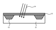
はじめに、本発明の実施の形態1を図1〜図8を参照して説明する。まず、図1に示す通り、シリコン基板11にSTI(shallow trench isolation)12を形成し、更に、犠牲酸化膜13を形成する。犠牲酸化膜13を介してウエル(Well)インプラ注入14を行う。次に、犠牲酸化膜13をエッチング除去し、その後、酸化膜形成前の洗浄処理を行う。
Hereinafter, some of the embodiments of the present invention will be described in detail with reference to the drawings.
(Embodiment 1)
First,
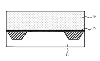
次に、図2に示す通り、シリコン基板11表面に任意の厚さのダミーゲート絶縁膜15を形成後、アモルファス或いはポリ状のシリコン膜、或いはシリコンゲルマニウム膜のダミーゲート電極16を堆積させる。
Next, as shown in FIG. 2, a dummy
次に、図3に示す通り、ダミーゲート電極16を加工後、エクステンション層111a及びハロー用の不純物をイオン注入し、更に、サイドウォール18を形成し、ソースドレイン用の不純物をイオン注入して、活性化アニールを施す。活性化アニールは、例えば約1050℃で数秒間のスパイクアニール(spikeアニール)とする。このようにして、浅接合のソースドレイン拡散層111を形成する。ここで、エクステンション層111aとソースドレイン拡散層111は同導電型の拡散層であり、ハローは逆導電型の拡散層となる。
Next, as shown in FIG. 3, after processing the
上記ソースドレイン拡散層111等を浅接合に形成する活性化アニールは、その他に、フラッシュランプアニール、レーザーアニール等のような低サーマルバジェットによる熱処理がある。ここで、フラッシュランプアニールにおいては、可視域から近赤外線域までの広い範囲に発光波長を有している白色光のキセノン(Xe)フラッシュランプを用いるとよい。このXeフラッシュランプは、数100μ秒〜数10m秒という極めて短時間の発光が可能な光源であり、その処理温度450〜600℃、処理時間10m秒程度で上記活性化アニールをすることができる。
The activation annealing for forming the source /
その後、図4に示す通り、例えばCo、Niなどの金属膜をスパッタ法で成膜し、公知のサリサイド技術によりソースドレイン拡散層111表面にシリサイド層19を低温で形成する。
Thereafter, as shown in FIG. 4, a metal film such as Co or Ni is formed by sputtering, and a
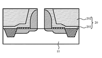
次に、図5に示す通り、窒化膜201と酸化膜202の層間膜20を形成する。下地の窒化膜201をストッパにCMP(Chemical Mechanical Polishing)を施し、アモルファス或いはポリ状のシリコン膜、或いはシリコンゲルマニウム膜のダミーゲート電極16を露出させ、ダミーゲート電極16をエッチングで除去し、シリコン基板11を露出させる。
Next, as shown in FIG. 5, an
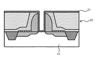
その後、図6に示す通り、例えばHfO2などのHigh−k材料をALD(Atomic Layer Deposition)或いはMOCVD法(Metal Organic Chemical Vapor Deposition)で堆積し、上記露出したシリコン基板11表面および層間膜20表面を被覆するhigh−k膜21を形成する。このようにして、高誘電体ゲート絶縁膜を構成する絶縁膜として、シリコン基板11上直にhigh−k膜21が形成される。
Thereafter, as shown in FIG. 6, a high-k material such as HfO 2 is deposited by ALD (Atomic Layer Deposition) or MOCVD (Metal Organic Chemical Vapor Deposition), and the exposed
ここで、high−k膜21としては、上述したところのHfO2の他にZrO2といった金属酸化物や、HfSiOx、ZrSiOxといった金属シリケート、HfAlOx、ZrAlOxといった金属アルミネート、La2O3、Y2O3等のランタノイド系元素の酸化物を主体とした高誘電率膜材料で構成すると好適である。そして、上記高誘電率膜材料から成るHigh−k膜のうち2種類以上の絶縁膜を選択し積層した積層構造の絶縁膜を用いてもよい。
Here, as the high-
この後、図7に示す通り、酸素雰囲気でプラズマ処理を施し、high−k膜21中の酸素欠損を補う。この処理により同時にシリコン基板11とhigh−k膜21の界面にSiO2界面形成膜22が形成される。このSiO2界面形成膜22は、400℃程度でサブナノメータ程度の膜厚に形成される。
Thereafter, as shown in FIG. 7, plasma treatment is performed in an oxygen atmosphere to compensate for oxygen vacancies in the high-
以上のようにして、高誘電体ゲート絶縁膜を構成するhigh−k膜21とSiO2界面形成膜22を形成後、フッ素を界面に導入する目的で、F2の雰囲気(窒素との混合比で1vol.%から10vol.%程度の濃度に希釈した雰囲気)中で、100℃から400℃まで昇温し、1分から10分程度保持したプロセスを経てF2アニール23を施す。このプロセスを取ることにより、フッ素添加時に特別なアニール処理を行わない。この処理によってhigh−k膜21、SiO2界面形成膜22中、そして特にシリコン基板11との界面付近に多くのフッ素が局在する状態を実現できる(図11参照)。この界面には、1020/cm3以上の量のフッ素が存在する。
After forming the high-
フッ素を導入するガス雰囲気としてF2を挙げたが、これはフッ素を含有する例えばフロロカーボン系ガス(CF4、C2F6、C3F8、C4F8、C4F4、C4F6、C5F8)やトリフルオロメタン(CHF3)、ジフルオロメタン(CH2F2)、六フッ化硫黄(SF6)、三フッ化窒素(NF3)、三フッ化塩素(ClF3)でも同様の効果が確認されている。但し、400℃以下の低温で実現するためには、F2が望ましい。 It has been mentioned the F 2 as the gas atmosphere introducing fluorine, this example fluorocarbon-based gas containing fluorine (CF 4, C 2 F 6 , C 3 F 8, C 4 F 8, C 4 F 4, C 4 F 6, C 5 F 8) and trifluoromethane (CHF 3), difluoromethane (CH 2 F 2), sulfur hexafluoride (SF 6), nitrogen trifluoride (NF 3), chlorine trifluoride (ClF 3 ), The same effect has been confirmed. However, F 2 is desirable for realizing at a low temperature of 400 ° C. or lower.
あるいは、上記NF3ガス、F2ガスをプラズマ励起し、このプラズマ励起で生成するフッ素の活性種の中でイオン種を除き、フッ素の中性ラジカルを上記high−k膜21表面に照射する、いわゆるフッ素のリモートプラズマ処理を施してもよい。この場合も、400℃以下の低温下にて、high−k膜21、SiO2界面形成膜22中、及びシリコン基板11との界面付近に多くのフッ素を導入させることができる。
Alternatively, the NF 3 gas and the F 2 gas are plasma-excited, the ionic species are removed from the active species of fluorine generated by the plasma excitation, and the surface of the high-
この後、図8に示す通り、例えばTiNまたはWなどのメタル膜をCVD法等で成膜し、公知のドライエッチング技術で加工してゲート電極24を形成し、ソースドレインのコンタクト25を形成し、配線材料工程を経て、例えばW、Alを用いて任意の回路を構成する。メタルゲート電極の形成など、high−k膜21形成後のプロセスは、600℃以下の低温で行われる。このように600℃以下の低温のプロセスにすることにより、高誘電体ゲート絶縁膜に含有されるフッ素の活性化は抑制されて安定化し、高品質の高誘電体ゲート絶縁膜および界面が得られるようになる。また、このように低温プロセスにすることで、high−k膜21の膜質劣化、シリサイド層19の凝集等の問題は皆無になる。
Thereafter, as shown in FIG. 8, a metal film such as TiN or W is formed by a CVD method or the like, processed by a known dry etching technique to form a
上記ゲート電極24としては、TiNの他に、ZrNx、HfNx、VNx、NbNx、TaNx、MoNx、WNx、あるいはTiSixNy、ZrSixNy、HfSixNy、VSixNy、NbSixNy、TaSixNy、MoSixNy、WSixNy等の導電体膜材料またはそれらの積層した材料を用いることができる。あるいは、Ti、Zr、Hf、V、Nb、Ta、Mo、Wなどの金属、TiSix、ZrSix、HfSix、VSix、NbSix、TaSix、MoSix、WSix、NiSix、CoSixなどの金属珪化物、TiCx、ZrCx、HfCx、VCx、NbCx、TaCx、MoCx、WCxなどの金属炭化物から成る導電体膜材料またはそれらの積層した材料を用いることができる。また、上記Wの代わりにAlやAl合金、CuやCu合金等を用いることができる。
As the
次に、上記実施の形態1の一実施例における効果について説明する。
フッ素処理をしたMISFETについて、ゲート領域は、W/TiN/HfO2(膜厚2.5nm)/SiO2(膜厚0.5nm)の構造に形成され、その形成工程の順序は、図1〜図8の通りである。ここで、上記フッ素ガスの処理により、高誘電体ゲート絶縁膜中のフッ素分布は図11に示すようになる。そして、ダミーゲート時のソースドレイン拡散層の活性化アニールは、1000℃、3秒程度であり、最終的なシンターは400℃である。また、フッ処理をしないMISFETは、フッ素アニール工程のみを行わず、その他の工程は同じである。
Next, effects in one example of the first embodiment will be described.
With respect to the MISFET subjected to the fluorine treatment, the gate region is formed in a structure of W / TiN / HfO 2 (film thickness 2.5 nm) / SiO 2 (film thickness 0.5 nm). It is as FIG. Here, the fluorine distribution in the high dielectric gate insulating film is as shown in FIG. 11 by the treatment of the fluorine gas. The activation annealing of the source / drain diffusion layer at the time of the dummy gate is 1000 ° C. for about 3 seconds, and the final sintering is 400 ° C. In addition, the MISFET that is not subjected to the fluorine treatment does not perform only the fluorine annealing process, and the other processes are the same.
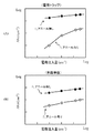
図9は、上記フッ素処理をした場合と、処理をしない場合のMISFETの移動度を示している。横軸が電界の強さ(Eeff(MV/cm))を示し、縦軸が移動度(μ(cm2/Vs))を示している。図9(A)は、N型MISFETの移動度を示し、図9(B)は、P型MISFETの移動度を示している。N型もP型もともにフッ素処理により移動度が向上している。N型MISFETは、P型MISFETより電界(横軸)全般に亘って移動度が向上しており、フッ素処理による効果がより多く得られていることを示している。 FIG. 9 shows the mobility of the MISFET with and without the fluorine treatment. The horizontal axis indicates the electric field strength (Eeff (MV / cm)), and the vertical axis indicates the mobility (μ (cm 2 / Vs)). FIG. 9A shows the mobility of the N-type MISFET, and FIG. 9B shows the mobility of the P-type MISFET. Both N-type and P-type have improved mobility by fluorine treatment. The N-type MISFET has improved mobility over the entire electric field (horizontal axis) as compared with the P-type MISFET, indicating that more effects are obtained by the fluorine treatment.
図10は、横軸の右部がフッ素系ガス処理を行った場合を示し、左部がフッ素系ガス処理を行わない場合を示している。右側の縦軸が界面準位(Dit(cm−2eV−1))を示し、左側の縦軸がNBTI(Negative Bias Temperature Instability)(ΔVth(V))を示している。白丸がN型MISFETを示し、黒丸がP型MISFETを示している。折れ線グラフは、右側の縦軸を利用し、N型とP型のMISFETの界面準位の相違を示している。棒グラフは、左側の縦軸を利用し、フッ素系ガス処理による、しきい値の変動を示している。 In FIG. 10, the right part of the horizontal axis shows the case where the fluorine-based gas treatment is performed, and the left part shows the case where the fluorine-based gas treatment is not performed. The vertical axis on the right side shows the interface state (Dit (cm −2 eV −1 )), and the vertical axis on the left side shows NBTI (Negative Bias Temperature Instability) (ΔVth (V)). White circles indicate N-type MISFETs, and black circles indicate P-type MISFETs. The line graph shows the difference in the interface state between the N-type and P-type MISFETs using the right vertical axis. The bar graph uses the vertical axis on the left side to show the variation of the threshold value due to the fluorine-based gas treatment.
図10に示す通り、N型もP型も、フッ素系ガス処理により、界面準位が低下しており、大きく改善していることが読み取れる。特に、N型の界面準位がP型より小さいことが分かる。また、フッ素系ガス処理により、しきい値の変動が小さくなっていることを示している。この結果、BTストレスを印加した場合、デバイスの信頼性の差も明らかであり、デバイス特性と信頼性の両方を同時に満足できることが確認される。 As shown in FIG. 10, it can be seen that both the N-type and P-type have greatly improved since the interface state is lowered by the fluorine-based gas treatment. In particular, it can be seen that the N-type interface state is smaller than the P-type. Moreover, it is shown that the fluctuation of the threshold value is reduced by the fluorine-based gas treatment. As a result, when BT stress is applied, the difference in device reliability is also clear, and it is confirmed that both device characteristics and reliability can be satisfied simultaneously.
図11は、シリコン基板11とゲート絶縁膜21、22との界面付近のフッ素の導入量を示しており、界面付近のフッ素の導入量は、1×10²⁰/cm3以上を示している。これにより、フッ素の導入量が界面付近で1×1020/cm3以上であると、より効果が得られることが知られる。
FIG. 11 shows the amount of fluorine introduced in the vicinity of the interface between the
(実施の形態2)
次に、本発明の実施の形態2を図1〜図6、図12〜図15を参照して説明する。この実施の形態の特徴は、実施の形態1において説明したhigh−k膜上に更に極薄絶縁膜を形成してから、上述したところのフッ素導入を行うところにある。あるいは、high−k膜上にフッ素を含有する極薄絶縁膜を積層して形成するところにある。このようにすることで、high−k膜と極薄絶縁膜との界面領域に更に多量のフッ素が容易に導入できるようになる。
(Embodiment 2)
Next, a second embodiment of the present invention will be described with reference to FIGS. 1 to 6 and FIGS. The feature of this embodiment resides in that after the ultra-thin insulating film is further formed on the high-k film described in the first embodiment, fluorine is introduced as described above. Alternatively, an ultra-thin insulating film containing fluorine is stacked on the high-k film. By doing so, a larger amount of fluorine can be easily introduced into the interface region between the high-k film and the ultrathin insulating film.
実施の形態2の場合においても、実施の形態1の場合と全く同様に、図1〜図6までの工程を経て、図6に示すダマシンゲートを構成するhigh−k膜21を成膜する。
In the case of the second embodiment, as in the case of the first embodiment, the high-
この後、図12に示す通り、酸素雰囲気でプラズマ処理を施し、high−k膜21中の酸素欠損を補う。同時に、この処理によりシリコン基板11とhigh−k膜21の界面にSiO2界面形成膜22が形成される。このSiO2界面形成膜22は、400℃程度で例えば0.5nm程度の膜厚に形成される。
Thereafter, as shown in FIG. 12, plasma treatment is performed in an oxygen atmosphere to compensate for oxygen vacancies in the high-
この後、図13に示す通り、例えばALD法により0.5nm〜1.5nm程度の膜厚の極薄絶縁膜26を形成する。上記ALD法において、例えばジクロールシランガス(SiH2Cl2)、水(H2O)等を成膜原料のプリカーサとして使用しシリコン酸化膜を成膜温度200〜300℃程度で堆積させる。この場合、high−k膜21を成膜するALD成膜装置と極薄絶縁膜26を成膜する成膜装置はマルチチャンバー構造になっており、high−k膜21と極薄絶縁膜26とを上記装置内で連続的に成膜するようにすれば好適である。ここで、極薄絶縁膜26としてシリコン窒化膜、シリコン酸窒化膜等を形成してもよい。シリコン窒化膜の成膜では、成膜原料のプリカーサとしてジクロールシランガス(SiH2Cl2)とアンモニア(NH3)を用いればよく、シリコン酸窒化膜の成膜におけるプリカーサとしてはジクロールシランガス(SiH2Cl2)、水(H2O)およびアンモニア(NH3)を使用する。
Thereafter, as shown in FIG. 13, an ultrathin insulating
以上のようにして、高誘電体ゲート絶縁膜を構成するhigh−k膜21、SiO2界面形成膜22および極薄絶縁膜26を形成後、実施の形態1の場合と同様に、図14に示す通り、F2ガスの雰囲気(窒素との混合比で1vol.%から10vol.%程度の濃度に希釈した雰囲気)中で、100℃から400℃まで昇温し、1分から10分程度保持したプロセスを経てF2アニール23を施す。このプロセスを取ることにより、フッ素添加時に特別なアニール処理を行わない。この処理によって極薄絶縁膜26とhigh−k膜21の界面、high−k膜21中、SiO2界面形成膜22中、及びシリコン基板11との界面付近に多くのフッ素が局在する状態を実現できる(図17参照)。これらの界面領域には、それぞれ3×10²¹/cm3程度、1×1020/cm3以上のフッ素量が含有されるようになる。しかも、図11と比較しても明らかなように、極薄絶縁膜26、high−k膜21およびSiO2界面形成膜22から成る高誘電体ゲート絶縁膜に、実施の形態1の場合よりも1桁以上多量のフッ素を導入することが可能になる。
As described above, after forming the high-
この場合も、実施の形態1の場合と同様に、フッ素を導入するガス雰囲気としてF2ガスの代わりにフッ素を含有する、例えばフロロカーボン系ガス(CF4、C2F6、C3F8、C4F8、C4F4、C4F6、C5F8)やトリフルオロメタン(CHF3)、ジフルオロメタン(CH2F2)、六フッ化硫黄(SF6)、三フッ化窒素(NF3)、三フッ化塩素(ClF3)でも同様の効果が生じる。あるいは、上記NF3ガス、F2ガスをプラズマ励起し、フッ素の活性種の中でイオン種を除き、フッ素の中性ラジカルを上記high−k膜21表面に照射する、いわゆるフッ素のリモートプラズマ処理を施してもよい。この場合も、400℃以下の低温下にて、high−k膜21、SiO2界面形成膜22中、及びシリコン基板11との界面付近に多くのフッ素を導入させることができる。
Also in this case, as in the first embodiment, fluorine gas is contained instead of F 2 gas as a gas atmosphere for introducing fluorine. For example, fluorocarbon-based gas (CF 4 , C 2 F 6 , C 3 F 8 , C 4 F 8, C 4 F 4, C 4 F 6, C 5 F 8) and trifluoromethane (CHF 3), difluoromethane (CH 2 F 2), sulfur hexafluoride (SF 6), nitrogen trifluoride (NF 3 ) and chlorine trifluoride (ClF 3 ) produce similar effects. Alternatively, so-called remote plasma treatment of fluorine in which the NF 3 gas and F 2 gas are plasma-excited, ion species are removed from the active species of fluorine, and the surface of the high-
また、極薄絶縁膜26の上記成膜においてフッ素をドープしてもよい。例えば上記ALD法の成膜時に上記プリカーサと共にドーピングガスとして希釈したF2ガス(窒素との混合比で0.1vol.%〜5vol.%程度)、NF3ガスあるいはSF6ガスを成膜室(チャンバー)に導入し、フッ素ドープの極薄絶縁膜26を成膜する。この方法においても、図17に示したのと同様の濃度分布を有し多量のフッ素を含有する高誘電体ゲート絶縁膜を形成することが可能になる。
Further, fluorine may be doped in the film formation of the ultrathin insulating
この後、図15に示す通り、実施の形態1と同様にして、例えばTiNまたはWなどのメタル膜から成るゲート電極24を形成し、更にソースドレインのコンタクト25を形成し、配線材料工程を経て、例えばW、Alを用いて任意の回路を構成する。メタルゲート電極の形成など、high−k膜21形成後のプロセスは、600℃以下の低温で行うと好適である。この600℃以下の低温のプロセスにすることにより、高誘電体ゲート絶縁膜に含有する多量のフッ素は不活性で安定化したままであり、高品質の高誘電体ゲート絶縁膜および界面が得られる。ここで、600℃温度を超えるプロセスを用いると、上記含有するフッ素は活性化し逆にシリコン基板との界面に損傷を与え易くなる。
Thereafter, as shown in FIG. 15, in the same manner as in the first embodiment, a
以下、上記実施の形態2の一実施例における効果について説明する。
上述したF2アニールによるフッ素処理をしたMISFETについて、ゲート領域は、W/TiN/SiN(膜厚0.5nm)/HfSiOx(膜厚2.0nm)/SiO2(膜厚0.5nm)の構造に形成され、その形成工程の順序は、図1〜図6、図12〜図15の通りである。ここで、上記F2アニールにより、高誘電体ゲート絶縁膜中のフッ素分布は図17に示すようになる。そして、ダミーゲート時の活性化アニールは、1000℃、3秒程度であり、最終的なシンターは400℃である。また、フッ処理をしないMISFETは、F2アニール工程のみを行わず、その他の工程は同じである。
Hereinafter, effects in one example of the second embodiment will be described.
In the MISFET subjected to the fluorine treatment by F 2 annealing described above, the gate region has a structure of W / TiN / SiN (film thickness 0.5 nm) / HfSiOx (film thickness 2.0 nm) / SiO 2 (film thickness 0.5 nm). The order of the forming steps is as shown in FIGS. 1 to 6 and 12 to 15. Here, the fluorine distribution in the high dielectric gate insulating film is as shown in FIG. 17 by the F 2 annealing. The activation annealing at the time of the dummy gate is about 1000 ° C. for about 3 seconds, and the final sintering is 400 ° C. In addition, the MISFET not subjected to the foot treatment does not perform only the F 2 annealing process, and the other processes are the same.
図16は、上記フッ素処理をした場合と、処理をしない場合のnチャネルMISFETの高誘電体ゲート絶縁膜中の電荷トラップ量と、上記高誘電体ゲート絶縁膜/シリコン基板界面の界面準位とを評価した結果を示している。この評価は、上記MISFETを公知のチャージポンピング法で測定して行った。ここで、図16(A)は、電荷トラップ量の評価結果を示し、図16(B)は、界面準位の評価結果を示している。図16(A、B)の横軸に高誘電体ゲート絶縁膜中への電荷注入量をとり、図16(A)の縦軸には高誘電体ゲート絶縁膜中への電荷注入により電荷トラップに捕獲された電荷キャリア数(トラップ電荷の増加量に対応している)を単位面積当たりで示す。そして、図16(B)の縦軸は高誘電体ゲート絶縁膜中への電荷注入ストレス(BTストレスに相当する)による界面準位密度の増加量を示している。 FIG. 16 shows the amount of charge traps in the high-dielectric gate insulating film of the n-channel MISFET with and without the fluorine treatment, and the interface state at the high-dielectric gate insulating film / silicon substrate interface. The result of evaluating is shown. This evaluation was performed by measuring the MISFET by a known charge pumping method. Here, FIG. 16A shows an evaluation result of the charge trap amount, and FIG. 16B shows an evaluation result of the interface state. In FIG. 16A and FIG. 16B, the horizontal axis represents the amount of charge injected into the high dielectric gate insulating film, and the vertical axis in FIG. 16A represents the charge trap by charge injection into the high dielectric gate insulating film. The number of charge carriers trapped in (corresponding to the increased amount of trapped charges) is shown per unit area. The vertical axis in FIG. 16B shows the amount of increase in interface state density due to charge injection stress (corresponding to BT stress) into the high dielectric gate insulating film.
図16(A)に示す通り、黒丸のフッ素処理をしないMISFETの場合は、白丸のフッ素処理をしたMISFETの場合よりも、電荷トラップは少なくとも1桁以上多く存在する。これは、上記実施の形態2で説明したようにMISFETの高誘電体ゲート絶縁膜中にフッ素を含有させることにより、膜中、特にhigh−k膜中の電荷トラップ量が1桁以上低減することを示している。 As shown in FIG. 16A, in the case of a MISFET that is not subjected to fluorine treatment of black circles, there are at least one digit more charge traps than in the case of a MISFET that is subjected to fluorine treatment of white circles. This is because the amount of charge traps in the film, particularly in the high-k film, is reduced by one digit or more by containing fluorine in the high dielectric gate insulating film of the MISFET as described in the second embodiment. Is shown.
図16(B)に示す通り、黒丸のフッ素処理をしないMISFETの場合は、白丸のフッ素処理をしたMISFETの場合よりも、上記ストレスによる界面準位の生成量は少なくとも1桁以上多くなる。これは、上記実施の形態2で説明したようにMISFETの高誘電体ゲート絶縁膜中にフッ素を含有させることにより、高誘電体ゲート絶縁膜/シリコン基板界面の結合状態が安定化することを示している。また、上記フッ素処理により、図10で説明したように界面準位は低下することは、実施の形態1の場合と全く同じである。上記図16で説明したフッ素処理の効果は、pチャネルMISFETの場合にも同様に生じるものである。 As shown in FIG. 16B, in the case of a MISFET that is not subjected to the fluorine treatment of black circles, the amount of interface state generated by the stress is at least one digit higher than that of the MISFET that is subjected to fluorine treatment of white circles. This indicates that, as described in the second embodiment, the coupling state of the high dielectric gate insulating film / silicon substrate interface is stabilized by containing fluorine in the high dielectric gate insulating film of the MISFET. ing. In addition, the interface state is lowered as described in FIG. 10 by the fluorine treatment, which is exactly the same as in the first embodiment. The effect of the fluorine treatment described with reference to FIG. 16 similarly occurs in the case of the p-channel MISFET.
図17は、実施の形態2特有の3層構造になる高誘電体ゲート絶縁膜へのフッ素の導入量を示している。図11と比較して判るように、この場合は、シリコン基板11とSiO2界面形成膜22、high−k膜21との界面付近、high−k膜21と極薄絶縁膜26との界面領域に多量のフッ素が蓄積(パイルアップ)する形態で含有される。そして、シリコン界面付近のフッ素の導入量は、1×10²⁰/cm3以上を示し、high−k膜21と極薄絶縁膜26と界面付近のフッ素の導入量は、更に1桁以上の多い3×1021/cm3程度になる。
FIG. 17 shows the amount of fluorine introduced into the high dielectric gate insulating film having a three-layer structure unique to the second embodiment. As can be seen from comparison with FIG. 11, in this case, the interface region between the
このようにhigh−k膜21を挟む上記2箇所の界面領域にフッ素が含有するようになるために、通常ではフッ素固溶度の小さいhigh−k膜21中であっても多量のフッ素を含有させることが可能になり、シリコン基板表面の界面準位の低減、膜中の電荷トラップの低減が容易に達成できるようになる。そして、高品質および信頼性の高い高誘電体ゲート絶縁膜の形成が可能になる。
As described above, since the fluorine is contained in the two interface regions sandwiching the high-
また、この実施の形態2の場合には、上記メカニズムによりhigh−k膜21に充分なフッ素量を含有させることが可能になり、フッ素導入のプロセス余裕度が非常に高くなって導入フッ素量の調整/制御が容易になる。
Further, in the case of the second embodiment, the high-
本発明は、上記実施の形態に限定されるものでなく、発明の趣旨を逸脱しない範囲でいろいろの変形を採ることができる。例えば、上述したようなダマシン構造のゲート電極のMISFETの代わりに、通常の構造であるフラット構造のゲート電極を有するMISFETの形成の場合にも本発明は同様に適用できるものである。この場合、高誘電体ゲート絶縁膜を形成後に、MISFETのソースドレイン等の拡散層を形成する。そこで、high−k膜の耐熱性を高めるために窒素を膜中に含有させる方法を併用させるとよい。あるいは、ソースドレイン拡散層等の拡散層のアニール温度を低減するために、上述したようなフラッシュランプアニールまたは600℃程度での固相成長技術を併用すればよい。 The present invention is not limited to the embodiment described above, and various modifications can be made without departing from the spirit of the invention. For example, instead of the damascene gate electrode MISFET as described above, the present invention can be similarly applied to the formation of a MISFET having a flat gate electrode which is a normal structure. In this case, a diffusion layer such as a source / drain of the MISFET is formed after the high dielectric gate insulating film is formed. Therefore, in order to increase the heat resistance of the high-k film, a method of incorporating nitrogen into the film may be used in combination. Alternatively, in order to reduce the annealing temperature of the diffusion layer such as the source / drain diffusion layer, flash lamp annealing as described above or a solid phase growth technique at about 600 ° C. may be used in combination.
また、high−k膜に用いる金属酸化膜としては、その他にアルミナ膜(Al2O3膜)、酸化タンタル膜(Ta2O5膜)、チタン酸ストロンチウム膜(STO膜)、チタン酸バリウムストロンチウム膜(BST膜)のような金属酸化膜あるいはチタン酸ジルコン酸鉛膜(PZT膜)のような強誘電体膜を用いてもよい。そして、high−k膜に用いる金属シリケート膜としては、La2O3、Y2O3等のランタノイド系元素のシリケート膜あるいは高融点金属のシリケート膜、更には、これらのシリケート膜の複合したシリケート膜を用いてもよい。また、high−k膜に用いる金属アルミネート膜としては、La2O3、Y2O3等のランタノイド系元素のアルミネート膜あるいは高融点金属のアルミネート膜、更には、これらのアルミネート膜の複合膜を用いてもよい。あるいは、シリケート膜とアルミネート膜の複合膜を使用することもできる。 In addition, examples of the metal oxide film used for the high-k film include an alumina film (Al 2 O 3 film), a tantalum oxide film (Ta 2 O 5 film), a strontium titanate film (STO film), and a barium strontium titanate. A metal oxide film such as a film (BST film) or a ferroelectric film such as a lead zirconate titanate film (PZT film) may be used. As a metal silicate film used for the high-k film, a silicate film of a lanthanoid element such as La 2 O 3 or Y 2 O 3 or a silicate film of a refractory metal, or a composite silicate film of these silicate films is used. A membrane may be used. Moreover, as a metal aluminate film used for the high-k film, an aluminate film of a lanthanoid element such as La 2 O 3 or Y 2 O 3 or an aluminate film of a refractory metal, and further these aluminate films The composite membrane may be used. Alternatively, a composite film of a silicate film and an aluminate film can be used.
また、上記極薄絶縁膜26として、high−k膜21とは異種の高誘電率膜を積層して形成させてもよい。この場合でも、実施の形態2のメカニズムが同様に働き、これらの異種high−k膜の界面にフッ素がパイルアップするために、多量のフッ素を高誘電体ゲート絶縁膜に含有させることができるようになる。
Further, the ultrathin insulating
11・・・シリコン基板
111a・・エクステンション層、ハロー層
111・・・ソースドレイン拡散層
12・・・STI(shallow trench isolation)
13・・・犠牲酸化膜
14・・・ウエルインプラ注入
15・・・ダミーゲート絶縁膜
16・・・ダミーゲート電極
18・・・サイドウォール
19・・・シリサイド層
20・・・層間膜
201・・層間膜(窒化膜)
202・・層間膜(酸化膜)
21・・・high−k膜
22・・・SiO2界面形成膜
23・・・F2アニール
24・・・メタルゲート電極
25・・・コンタクト電極
26・・・極薄絶縁膜
11...
13 ...
202 .. Interlayer film (oxide film)
21 ... high-
Claims (8)
Priority Applications (1)
| Application Number | Priority Date | Filing Date | Title |
|---|---|---|---|
| JP2004301462A JP2006114747A (en) | 2004-10-15 | 2004-10-15 | Method for manufacturing semiconductor device |
Applications Claiming Priority (1)
| Application Number | Priority Date | Filing Date | Title |
|---|---|---|---|
| JP2004301462A JP2006114747A (en) | 2004-10-15 | 2004-10-15 | Method for manufacturing semiconductor device |
Related Child Applications (1)
| Application Number | Title | Priority Date | Filing Date |
|---|---|---|---|
| JP2011004584A Division JP4985855B2 (en) | 2011-01-13 | 2011-01-13 | Manufacturing method of semiconductor device |
Publications (2)
| Publication Number | Publication Date |
|---|---|
| JP2006114747A true JP2006114747A (en) | 2006-04-27 |
| JP2006114747A5 JP2006114747A5 (en) | 2007-11-22 |
Family
ID=36383007
Family Applications (1)
| Application Number | Title | Priority Date | Filing Date |
|---|---|---|---|
| JP2004301462A Withdrawn JP2006114747A (en) | 2004-10-15 | 2004-10-15 | Method for manufacturing semiconductor device |
Country Status (1)
| Country | Link |
|---|---|
| JP (1) | JP2006114747A (en) |
Cited By (9)
| Publication number | Priority date | Publication date | Assignee | Title |
|---|---|---|---|---|
| JP2008078253A (en) * | 2006-09-20 | 2008-04-03 | Sony Corp | Manufacturing method of semiconductor device |
| JP2008530770A (en) * | 2005-01-13 | 2008-08-07 | インターナショナル・ビジネス・マシーンズ・コーポレーション | Method for forming HfSiN metal for n-FET applications |
| JP2008311661A (en) * | 2007-06-15 | 2008-12-25 | Dongbu Hitek Co Ltd | Semiconductor element and its gate forming method |
| JP2010505281A (en) * | 2006-09-26 | 2010-02-18 | アプライド マテリアルズ インコーポレイテッド | Fluorine plasma treatment for high-K gate stacks for defect passivation |
| JP2010212376A (en) * | 2009-03-09 | 2010-09-24 | Toshiba Corp | Method of manufacturing semiconductor device |
| JP2011103459A (en) * | 2009-10-07 | 2011-05-26 | Asm Internatl Nv | Method of adjusting threshold voltage of gate stack of pmos device |
| US8431468B2 (en) | 2006-12-07 | 2013-04-30 | Infineon Technologies Ag | Noise reduction in semiconductor devices |
| JP2013175769A (en) * | 2006-12-11 | 2013-09-05 | Sony Corp | Manufacturing method of semiconductor device |
| CN104347503A (en) * | 2013-07-30 | 2015-02-11 | 中芯国际集成电路制造(上海)有限公司 | Semiconductor device and manufacturing method thereof |
Citations (9)
| Publication number | Priority date | Publication date | Assignee | Title |
|---|---|---|---|---|
| JPH0685278A (en) * | 1992-09-07 | 1994-03-25 | Hitachi Ltd | Manufacture of semiconductor device |
| JPH09266308A (en) * | 1996-03-29 | 1997-10-07 | Nec Corp | Method of manufacturing semiconductor device |
| JPH1140803A (en) * | 1997-07-15 | 1999-02-12 | Toshiba Corp | Semiconductor device and its manufacture |
| JP2000022139A (en) * | 1998-06-30 | 2000-01-21 | Toshiba Corp | Semiconductor device and its manufacture |
| JP2002299614A (en) * | 2001-03-30 | 2002-10-11 | Toshiba Corp | Mis field effect transistor, method for manufacturing it, semiconductor storage medium and method for manufacturing it |
| JP2003218082A (en) * | 2002-01-23 | 2003-07-31 | Tokyo Electron Ltd | Substrate-treating method and apparatus, and manufacturing apparatus of semiconductor device |
| WO2003100835A2 (en) * | 2002-05-20 | 2003-12-04 | Advanced Micro Devices, Inc. | Gate oxide process methods for high performance mos transistors by reducing remote scattering |
| JP2004193150A (en) * | 2002-12-06 | 2004-07-08 | Toshiba Corp | Semiconductor device and its manufacturing method |
| JP2004207560A (en) * | 2002-12-26 | 2004-07-22 | Toshiba Corp | Semiconductor device and its manufacturing method |
-
2004
- 2004-10-15 JP JP2004301462A patent/JP2006114747A/en not_active Withdrawn
Patent Citations (9)
| Publication number | Priority date | Publication date | Assignee | Title |
|---|---|---|---|---|
| JPH0685278A (en) * | 1992-09-07 | 1994-03-25 | Hitachi Ltd | Manufacture of semiconductor device |
| JPH09266308A (en) * | 1996-03-29 | 1997-10-07 | Nec Corp | Method of manufacturing semiconductor device |
| JPH1140803A (en) * | 1997-07-15 | 1999-02-12 | Toshiba Corp | Semiconductor device and its manufacture |
| JP2000022139A (en) * | 1998-06-30 | 2000-01-21 | Toshiba Corp | Semiconductor device and its manufacture |
| JP2002299614A (en) * | 2001-03-30 | 2002-10-11 | Toshiba Corp | Mis field effect transistor, method for manufacturing it, semiconductor storage medium and method for manufacturing it |
| JP2003218082A (en) * | 2002-01-23 | 2003-07-31 | Tokyo Electron Ltd | Substrate-treating method and apparatus, and manufacturing apparatus of semiconductor device |
| WO2003100835A2 (en) * | 2002-05-20 | 2003-12-04 | Advanced Micro Devices, Inc. | Gate oxide process methods for high performance mos transistors by reducing remote scattering |
| JP2004193150A (en) * | 2002-12-06 | 2004-07-08 | Toshiba Corp | Semiconductor device and its manufacturing method |
| JP2004207560A (en) * | 2002-12-26 | 2004-07-22 | Toshiba Corp | Semiconductor device and its manufacturing method |
Cited By (18)
| Publication number | Priority date | Publication date | Assignee | Title |
|---|---|---|---|---|
| JP2008530770A (en) * | 2005-01-13 | 2008-08-07 | インターナショナル・ビジネス・マシーンズ・コーポレーション | Method for forming HfSiN metal for n-FET applications |
| JP2008078253A (en) * | 2006-09-20 | 2008-04-03 | Sony Corp | Manufacturing method of semiconductor device |
| JP2010505281A (en) * | 2006-09-26 | 2010-02-18 | アプライド マテリアルズ インコーポレイテッド | Fluorine plasma treatment for high-K gate stacks for defect passivation |
| US8431468B2 (en) | 2006-12-07 | 2013-04-30 | Infineon Technologies Ag | Noise reduction in semiconductor devices |
| US11901454B2 (en) | 2006-12-11 | 2024-02-13 | Sony Group Corporation | Metal oxide semiconductor having epitaxial source drain regions and a method of manufacturing same using dummy gate process |
| US10868176B2 (en) | 2006-12-11 | 2020-12-15 | Sony Corporation | Metal oxide semiconductor having epitaxial source drain regions and a method of manufacturing same using dummy gate process |
| JP2013175769A (en) * | 2006-12-11 | 2013-09-05 | Sony Corp | Manufacturing method of semiconductor device |
| US11404573B2 (en) | 2006-12-11 | 2022-08-02 | Sony Group Corporation | Metal oxide semiconductor having epitaxial source drain regions and a method of manufacturing same using dummy gate process |
| US9041058B2 (en) | 2006-12-11 | 2015-05-26 | Sony Corporation | Metal oxide semiconductor having epitaxial source drain regions and method of manufacturing same using dummy gate process |
| US9419096B2 (en) | 2006-12-11 | 2016-08-16 | Sony Corporation | Metal oxide semiconductor having epitaxial source drain regions and a method of manufacturing same using dummy gate process |
| US9502529B2 (en) | 2006-12-11 | 2016-11-22 | Sony Corporation | Metal oxide semiconductor having epitaxial source drain regions and a method of manufacturing same using dummy gate process |
| US9673326B2 (en) | 2006-12-11 | 2017-06-06 | Sony Corporation | Metal oxide semiconductor having epitaxial source drain regions and a method of manufacturing same using dummy gate process |
| US9865733B2 (en) | 2006-12-11 | 2018-01-09 | Sony Corporation | Metal oxide semiconductor having epitaxial source drain regions and a method of manufacturing same using dummy gate process |
| US10128374B2 (en) | 2006-12-11 | 2018-11-13 | Sony Corporation | Metal oxide semiconductor having epitaxial source drain regions and a method of manufacturing same using dummy gate process |
| JP2008311661A (en) * | 2007-06-15 | 2008-12-25 | Dongbu Hitek Co Ltd | Semiconductor element and its gate forming method |
| JP2010212376A (en) * | 2009-03-09 | 2010-09-24 | Toshiba Corp | Method of manufacturing semiconductor device |
| JP2011103459A (en) * | 2009-10-07 | 2011-05-26 | Asm Internatl Nv | Method of adjusting threshold voltage of gate stack of pmos device |
| CN104347503A (en) * | 2013-07-30 | 2015-02-11 | 中芯国际集成电路制造(上海)有限公司 | Semiconductor device and manufacturing method thereof |
Similar Documents
| Publication | Publication Date | Title |
|---|---|---|
| US10535748B2 (en) | Method of forming a contact with a silicide region | |
| US6911707B2 (en) | Ultrathin high-K gate dielectric with favorable interface properties for improved semiconductor device performance | |
| US9147614B2 (en) | Transistor device and fabrication method | |
| KR101878696B1 (en) | Methods to integrate sonos into cmos flow | |
| JP5811432B2 (en) | Semiconductor structure for trapping impurity oxygen for high-k gate dielectric and method for forming the structure (trapping metal stack for high-k gate dielectric) | |
| US9698269B2 (en) | Conformal nitridation of one or more fin-type transistor layers | |
| US8889505B2 (en) | Method for manufacturing semiconductor device | |
| JP2006108602A (en) | Semiconductor device and its manufacturing method | |
| US9105720B2 (en) | Semiconductor device having metal gate and manufacturing method thereof | |
| US11101178B2 (en) | Semiconductor integrated circuit | |
| US9385208B2 (en) | Semiconductor device having high-K gate dielectric layer | |
| US7939396B2 (en) | Base oxide engineering for high-K gate stacks | |
| US20180337248A1 (en) | High-K Dielectric and Method of Manufacture | |
| JP2006114747A (en) | Method for manufacturing semiconductor device | |
| JP4985855B2 (en) | Manufacturing method of semiconductor device | |
| US20140035058A1 (en) | Semiconductor Devices and Methods of Manufacturing the Same | |
| JP2008072001A (en) | Semiconductor device and manufacturing method therefor | |
| KR100712523B1 (en) | Semiconductor device having different gate dielectric layers and method for manufacturing the same | |
| JP2005079390A (en) | Semiconductor device | |
| JP2007142007A (en) | Semiconductor device and manufacturing method thereof | |
| JP2006073704A (en) | Manufacturing method of semiconductor apparatus | |
| KR101623462B1 (en) | METHOD OF MANUFACTURING SEMICONDUCTOR DEVICE COMPRISING HIGH-k METAL OXIDE FILM | |
| JP2006080354A (en) | Manufacturing method of misfet | |
| JP2005347584A (en) | Method of manufacturing semiconductor device | |
| JP2012109339A (en) | Method of manufacturing semiconductor device |
Legal Events
| Date | Code | Title | Description |
|---|---|---|---|
| A521 | Request for written amendment filed |
Free format text: JAPANESE INTERMEDIATE CODE: A523 Effective date: 20071009 |
|
| A621 | Written request for application examination |
Free format text: JAPANESE INTERMEDIATE CODE: A621 Effective date: 20071009 |
|
| A977 | Report on retrieval |
Free format text: JAPANESE INTERMEDIATE CODE: A971007 Effective date: 20080327 |
|
| A131 | Notification of reasons for refusal |
Free format text: JAPANESE INTERMEDIATE CODE: A131 Effective date: 20100727 |
|
| A521 | Request for written amendment filed |
Free format text: JAPANESE INTERMEDIATE CODE: A523 Effective date: 20100921 |
|
| A131 | Notification of reasons for refusal |
Free format text: JAPANESE INTERMEDIATE CODE: A131 Effective date: 20101116 |
|
| A761 | Written withdrawal of application |
Free format text: JAPANESE INTERMEDIATE CODE: A761 Effective date: 20110118 |