US9147614B2 - Transistor device and fabrication method - Google Patents

Transistor device and fabrication method Download PDF

Info

Publication number
US9147614B2
US9147614B2 US13/904,341 US201313904341A US9147614B2 US 9147614 B2 US9147614 B2 US 9147614B2 US 201313904341 A US201313904341 A US 201313904341A US 9147614 B2 US9147614 B2 US 9147614B2
Authority
US
United States
Prior art keywords
dielectric layer
layer
forming
dummy gate
semiconductor substrate
Prior art date
Legal status (The legal status is an assumption and is not a legal conclusion. Google has not performed a legal analysis and makes no representation as to the accuracy of the status listed.)
Active, expires
Application number
US13/904,341
Other versions
US20140077313A1 (en
Inventor
Aileen Li
Jinghua Ni
Current Assignee (The listed assignees may be inaccurate. Google has not performed a legal analysis and makes no representation or warranty as to the accuracy of the list.)
Semiconductor Manufacturing International Corp
Original Assignee
Semiconductor Manufacturing International Corp
Priority date (The priority date is an assumption and is not a legal conclusion. Google has not performed a legal analysis and makes no representation as to the accuracy of the date listed.)
Filing date
Publication date
Application filed by Semiconductor Manufacturing International Corp filed Critical Semiconductor Manufacturing International Corp
Assigned to SEMICONDUCTOR MANUFACTURING INTERNATIONAL CORP. reassignment SEMICONDUCTOR MANUFACTURING INTERNATIONAL CORP. ASSIGNMENT OF ASSIGNORS INTEREST (SEE DOCUMENT FOR DETAILS). Assignors: LI, AILEEN, NI, JINGHUA
Publication of US20140077313A1 publication Critical patent/US20140077313A1/en
Application granted granted Critical
Publication of US9147614B2 publication Critical patent/US9147614B2/en
Active legal-status Critical Current
Adjusted expiration legal-status Critical

Links

Images

Classifications

    • HELECTRICITY
    • H01ELECTRIC ELEMENTS
    • H01LSEMICONDUCTOR DEVICES NOT COVERED BY CLASS H10
    • H01L21/00Processes or apparatus adapted for the manufacture or treatment of semiconductor or solid state devices or of parts thereof
    • H01L21/70Manufacture or treatment of devices consisting of a plurality of solid state components formed in or on a common substrate or of parts thereof; Manufacture of integrated circuit devices or of parts thereof
    • H01L21/77Manufacture or treatment of devices consisting of a plurality of solid state components or integrated circuits formed in, or on, a common substrate
    • H01L21/78Manufacture or treatment of devices consisting of a plurality of solid state components or integrated circuits formed in, or on, a common substrate with subsequent division of the substrate into plural individual devices
    • H01L21/82Manufacture or treatment of devices consisting of a plurality of solid state components or integrated circuits formed in, or on, a common substrate with subsequent division of the substrate into plural individual devices to produce devices, e.g. integrated circuits, each consisting of a plurality of components
    • H01L21/822Manufacture or treatment of devices consisting of a plurality of solid state components or integrated circuits formed in, or on, a common substrate with subsequent division of the substrate into plural individual devices to produce devices, e.g. integrated circuits, each consisting of a plurality of components the substrate being a semiconductor, using silicon technology
    • H01L21/8232Field-effect technology
    • H01L21/8234MIS technology, i.e. integration processes of field effect transistors of the conductor-insulator-semiconductor type
    • H01L21/8238Complementary field-effect transistors, e.g. CMOS
    • H01L21/823828Complementary field-effect transistors, e.g. CMOS with a particular manufacturing method of the gate conductors, e.g. particular materials, shapes
    • H01L21/823842Complementary field-effect transistors, e.g. CMOS with a particular manufacturing method of the gate conductors, e.g. particular materials, shapes gate conductors with different gate conductor materials or different gate conductor implants, e.g. dual gate structures
    • HELECTRICITY
    • H01ELECTRIC ELEMENTS
    • H01LSEMICONDUCTOR DEVICES NOT COVERED BY CLASS H10
    • H01L21/00Processes or apparatus adapted for the manufacture or treatment of semiconductor or solid state devices or of parts thereof
    • H01L21/02Manufacture or treatment of semiconductor devices or of parts thereof
    • H01L21/04Manufacture or treatment of semiconductor devices or of parts thereof the devices having at least one potential-jump barrier or surface barrier, e.g. PN junction, depletion layer or carrier concentration layer
    • H01L21/18Manufacture or treatment of semiconductor devices or of parts thereof the devices having at least one potential-jump barrier or surface barrier, e.g. PN junction, depletion layer or carrier concentration layer the devices having semiconductor bodies comprising elements of Group IV of the Periodic System or AIIIBV compounds with or without impurities, e.g. doping materials
    • H01L21/28Manufacture of electrodes on semiconductor bodies using processes or apparatus not provided for in groups H01L21/20 - H01L21/268
    • H01L21/28008Making conductor-insulator-semiconductor electrodes
    • H01L21/28017Making conductor-insulator-semiconductor electrodes the insulator being formed after the semiconductor body, the semiconductor being silicon
    • H01L21/28158Making the insulator
    • H01L21/28167Making the insulator on single crystalline silicon, e.g. using a liquid, i.e. chemical oxidation
    • H01L21/28185Making the insulator on single crystalline silicon, e.g. using a liquid, i.e. chemical oxidation with a treatment, e.g. annealing, after the formation of the gate insulator and before the formation of the definitive gate conductor
    • HELECTRICITY
    • H01ELECTRIC ELEMENTS
    • H01LSEMICONDUCTOR DEVICES NOT COVERED BY CLASS H10
    • H01L21/00Processes or apparatus adapted for the manufacture or treatment of semiconductor or solid state devices or of parts thereof
    • H01L21/02Manufacture or treatment of semiconductor devices or of parts thereof
    • H01L21/04Manufacture or treatment of semiconductor devices or of parts thereof the devices having at least one potential-jump barrier or surface barrier, e.g. PN junction, depletion layer or carrier concentration layer
    • H01L21/18Manufacture or treatment of semiconductor devices or of parts thereof the devices having at least one potential-jump barrier or surface barrier, e.g. PN junction, depletion layer or carrier concentration layer the devices having semiconductor bodies comprising elements of Group IV of the Periodic System or AIIIBV compounds with or without impurities, e.g. doping materials
    • H01L21/28Manufacture of electrodes on semiconductor bodies using processes or apparatus not provided for in groups H01L21/20 - H01L21/268
    • H01L21/28008Making conductor-insulator-semiconductor electrodes
    • H01L21/28017Making conductor-insulator-semiconductor electrodes the insulator being formed after the semiconductor body, the semiconductor being silicon
    • H01L21/28158Making the insulator
    • H01L21/28167Making the insulator on single crystalline silicon, e.g. using a liquid, i.e. chemical oxidation
    • H01L21/28194Making the insulator on single crystalline silicon, e.g. using a liquid, i.e. chemical oxidation by deposition, e.g. evaporation, ALD, CVD, sputtering, laser deposition
    • HELECTRICITY
    • H01ELECTRIC ELEMENTS
    • H01LSEMICONDUCTOR DEVICES NOT COVERED BY CLASS H10
    • H01L29/00Semiconductor devices adapted for rectifying, amplifying, oscillating or switching, or capacitors or resistors with at least one potential-jump barrier or surface barrier, e.g. PN junction depletion layer or carrier concentration layer; Details of semiconductor bodies or of electrodes thereof  ; Multistep manufacturing processes therefor
    • H01L29/40Electrodes ; Multistep manufacturing processes therefor
    • H01L29/43Electrodes ; Multistep manufacturing processes therefor characterised by the materials of which they are formed
    • H01L29/49Metal-insulator-semiconductor electrodes, e.g. gates of MOSFET
    • H01L29/51Insulating materials associated therewith
    • H01L29/517Insulating materials associated therewith the insulating material comprising a metallic compound, e.g. metal oxide, metal silicate
    • HELECTRICITY
    • H01ELECTRIC ELEMENTS
    • H01LSEMICONDUCTOR DEVICES NOT COVERED BY CLASS H10
    • H01L29/00Semiconductor devices adapted for rectifying, amplifying, oscillating or switching, or capacitors or resistors with at least one potential-jump barrier or surface barrier, e.g. PN junction depletion layer or carrier concentration layer; Details of semiconductor bodies or of electrodes thereof  ; Multistep manufacturing processes therefor
    • H01L29/66Types of semiconductor device ; Multistep manufacturing processes therefor
    • H01L29/66007Multistep manufacturing processes
    • H01L29/66075Multistep manufacturing processes of devices having semiconductor bodies comprising group 14 or group 13/15 materials
    • H01L29/66227Multistep manufacturing processes of devices having semiconductor bodies comprising group 14 or group 13/15 materials the devices being controllable only by the electric current supplied or the electric potential applied, to an electrode which does not carry the current to be rectified, amplified or switched, e.g. three-terminal devices
    • H01L29/66409Unipolar field-effect transistors
    • H01L29/66477Unipolar field-effect transistors with an insulated gate, i.e. MISFET
    • H01L29/66545Unipolar field-effect transistors with an insulated gate, i.e. MISFET using a dummy, i.e. replacement gate in a process wherein at least a part of the final gate is self aligned to the dummy gate
    • HELECTRICITY
    • H01ELECTRIC ELEMENTS
    • H01LSEMICONDUCTOR DEVICES NOT COVERED BY CLASS H10
    • H01L29/00Semiconductor devices adapted for rectifying, amplifying, oscillating or switching, or capacitors or resistors with at least one potential-jump barrier or surface barrier, e.g. PN junction depletion layer or carrier concentration layer; Details of semiconductor bodies or of electrodes thereof  ; Multistep manufacturing processes therefor
    • H01L29/66Types of semiconductor device ; Multistep manufacturing processes therefor
    • H01L29/68Types of semiconductor device ; Multistep manufacturing processes therefor controllable by only the electric current supplied, or only the electric potential applied, to an electrode which does not carry the current to be rectified, amplified or switched
    • H01L29/76Unipolar devices, e.g. field effect transistors
    • H01L29/772Field effect transistors
    • H01L29/78Field effect transistors with field effect produced by an insulated gate
    • HELECTRICITY
    • H01ELECTRIC ELEMENTS
    • H01LSEMICONDUCTOR DEVICES NOT COVERED BY CLASS H10
    • H01L29/00Semiconductor devices adapted for rectifying, amplifying, oscillating or switching, or capacitors or resistors with at least one potential-jump barrier or surface barrier, e.g. PN junction depletion layer or carrier concentration layer; Details of semiconductor bodies or of electrodes thereof  ; Multistep manufacturing processes therefor
    • H01L29/40Electrodes ; Multistep manufacturing processes therefor
    • H01L29/43Electrodes ; Multistep manufacturing processes therefor characterised by the materials of which they are formed
    • H01L29/49Metal-insulator-semiconductor electrodes, e.g. gates of MOSFET
    • H01L29/51Insulating materials associated therewith
    • H01L29/511Insulating materials associated therewith with a compositional variation, e.g. multilayer structures
    • H01L29/513Insulating materials associated therewith with a compositional variation, e.g. multilayer structures the variation being perpendicular to the channel plane

Definitions

  • the present disclosure relates to the field of semiconductor technology and, more particularly, relates to metal gate structures, MOS transistors, and CMOS transistors and their fabrication methods.
  • MOS metal-oxide-semiconductor
  • the thickness of gate dielectric layers in the MOS transistors has become thinner and thinner.
  • various issues may occur. These issues may include time-related voltage breakdowns, hot carrier effects, and diffusion of impurities from the gate electrode toward the substrate. This can adversely affect stability and reliability of the formed transistors.
  • use of SiO 2 as a gate dielectric material may reach its physical limitation. Replacing SiO 2 gate dielectric layer with high-k gate dielectric layer may significantly increase the physical thickness with the same effective oxide thickness (EOT) achieved to reduce leakage current of the gate electrode.
  • EOT effective oxide thickness
  • high-k gate dielectric layers are made of metal oxides, which do not have fixed atomic coordinates.
  • SiO 2 gate dielectric material high-k gate dielectric materials have much poorer bonding stability with the silicon substrate. Consequently, interfacial defects are formed between the high-k gate dielectric layer and the silicon substrate.
  • the interfacial defects may be combined with oxygen to produce interstitial oxygen atoms and positively charged oxygen vacancies, which may further be combined with hydrogen to form unstable hydrogen bonds.
  • Such unstable hydrogen bonds can cause a PMOS transistor to have negative bias temperature instability (NBTI). That is, at high temperatures and when the gate electrode is negatively biased, electrical parameter drift of the PMOS transistor may occur.
  • NBTI negative bias temperature instability
  • the interstitial oxygen atoms and positively charged oxygen vacancies can cause an NMOS transistor to have positive bias temperature instability (PBTI). That is, at high temperatures and when the gate electrode is positively biased, electrical parameter drift of the NMOS transistor may occur.
  • PBTI positive bias temperature instability
  • a method for forming a transistor in this method, a dummy gate and an interlayer dielectric layer can be formed over a semiconductor substrate. A top surface of the dummy gate can be flush with a top surface of the interlayer dielectric layer. The dummy gate can then be removed to form a trench over the semiconductor substrate. A high-k dielectric layer can be conformally formed over each surface of the trench and the interlayer dielectric layer. The high-k dielectric layer can be fluorinated to form a fluorinated high-k dielectric layer. A functional layer can be formed on the fluorinated high-k dielectric layer and a metal layer can be formed on the functional layer to fill the trench with the metal layer. The interlayer dielectric layer can be exposed by polishing the metal layer, the functional layer, and the fluorinated high-k dielectric layer on the interlayer dielectric layer.
  • a semiconductor substrate can be provided to include a first region and a second region.
  • the first region can include a first dummy gate formed on the semiconductor substrate.
  • the second region can include a second dummy gate formed on the semiconductor substrate.
  • An interlayer dielectric layer can be formed over the semiconductor substrate.
  • the interlayer dielectric layer can have a top surface flushed with a top surface of each of the first and the second dummy gates.
  • the first dummy gate can be removed to form a first trench, and the second dummy gate can be removed to form a second trench.
  • a high-k dielectric layer can be conformally formed over each surface of the first trench, the second trench, and the interlayer dielectric layer.
  • the high-k dielectric layer can be fluorinated to form a fluorinated high-k dielectric layer.
  • a first functional layer can be formed on the fluorinated high-k dielectric layer in the first region and a second functional layer can be formed on the fluorinated high-k dielectric layer in the second region.
  • the first functional layer and the second functional layer can have different work functions.
  • a metal layer can be formed on the first and second functional layers to fill each of the first trench and the second trench.
  • the interlayer dielectric layer can be exposed by a surface planarization process.
  • a transistor can include an interlayer dielectric layer disposed over a semiconductor substrate.
  • the interlayer dielectric layer can include a trench disposed in the interlayer dielectric layer and over the semiconductor substrate.
  • a fluorinated high-k dielectric layer can be disposed conformally over a surface of the trench.
  • a functional layer can be disposed on the fluorinated high-k dielectric layer.
  • a metal layer can be disposed on the functional layer to fill the trench in the functional layer to form a gate electrode.
  • FIGS. 1-8 are schematics of cross-sectional views of an exemplary MOS transistor at various stages during its formation in accordance with various disclosed embodiments
  • FIGS. 9-16 are schematics of cross-sectional views of an exemplary CMOS device at various stages during its formation in accordance with various disclosed embodiments.
  • FIG. 17 compares lifetime of an exemplary NMOS transistor formed with and without a fluorination treatment in accordance with various disclosed embodiments
  • FIG. 18 compares lifetime of an exemplary PMOS transistor formed with and without a fluorination treatment in accordance with various disclosed embodiments
  • FIG. 19 depicts an exemplary method for forming an exemplary MOS transistor in accordance with various disclosed embodiments.
  • FIG. 20 depicts an exemplary method for forming an exemplary CMOS transistor in accordance with various disclosed embodiments.
  • high-k dielectric layers can be treated, e.g., fluorinated, during formation of a metal gate structure.
  • a trench can be formed by removing a dummy gate.
  • a high-k gate dielectric layer can be conformally formed on the bottom and sidewall of the trench and can be fluorinated so that fluorine bonds (e.g., F—Si, F—Hf, etc.) can be formed between high-k gate dielectric layer and the semiconductor substrate.
  • fluorine bonds have higher bond energy than hydrogen bonds generated between untreated high-k gate dielectric layer and the semiconductor substrate, NBTI of the subsequently-formed transistor can be reduced.
  • fluorine is a strong oxidant, it can prevent oxygen vacancies from producing donor levels in band gaps and prevent oxygen vacancies from being positively charged. As a result, the oxygen vacancies can be passivated and PBTI of the subsequently-formed transistor can be reduced.
  • FIGS. 1-8 are schematics of cross-sectional views of an exemplary MOS transistor, while FIG. 19 depicts an exemplary method for forming an exemplary MOS transistor in accordance with various disclosed embodiments. Note that although FIGS. 1-8 depict structures corresponding to the method depicted in FIG. 19 , the structures and the method are not limited to each other in any manner.
  • Step 1910 of FIG. 19 and referring to FIG. 1 there is provided a semiconductor substrate 100 .
  • a second silicon oxide layer 115 can be formed on the semiconductor substrate 100 .
  • a source region 121 and a drain region 122 can be formed in the semiconductor substrate 100 on both sides of the dummy gate 110 .
  • the semiconductor substrate 100 can be, e.g., silicon, germanium, silicon nitride, and/or silicon-on-insulator (SOI). Depending on specific semiconductor device to be formed thereon, certain substrate can be selected.
  • SOI silicon-on-insulator
  • a dummy gate 110 can be formed on the second silicon oxide layer 115 .
  • the second silicon oxide layer 115 is formed between the dummy gate 110 and the semiconductor substrate 100 to prevent direct contact between the semiconductor substrate and the subsequently formed high-k gate dielectric layer, because such direct contact can produce defects due to lattice mismatch.
  • the second silicon oxide layer may not be formed between the dummy gate 110 and the semiconductor substrate 100 .
  • Sidewall spacers may be formed on sidewall of the dummy gate and can be used as a mask for ion implantations to form source and drain regions.
  • ion implantations can be performed to form a source region 121 and a drain region 122 in the semiconductor substrate on both sides of dummy gate 110 .
  • silicon-containing stress layers e.g., silicon carbide or silicon-germanium
  • Carrier mobility can be improved by generating compressive stress or tensile stress in the channel region. Electrical performance of the MOS transistor can be improved.
  • an etch stop layer 135 can be formed on the semiconductor substrate 100 and the dummy gate 110 .
  • An interlayer dielectric (ILD) layer 130 can be formed on the etch stop layer 135 .
  • the interlayer dielectric layer 130 can be polished or planarized, e.g., by a chemical mechanical planarization (CMP), until a top surface of the dummy gate 110 is exposed and is flush with the top surface of the polished interlayer dielectric layer 130 .
  • CMP chemical mechanical planarization
  • the interlayer dielectric layer 130 can be made of a material including, e.g., silicon oxide, and/or low-k dielectric or ultra-low-k dielectric materials such as amorphous carbon, silicon-containing aerogels, etc. In one embodiment, the interlayer dielectric layer 130 is made of silicon oxide.
  • the etch stop layer 135 can be formed on the semiconductor substrate 100 and the dummy gate 110 , before the interlayer dielectric layer 130 is formed.
  • the etch stop layer 135 can be used as a barrier layer, when polishing the interlayer dielectric layer 130 to expose the dummy gate 110 .
  • the etch stop layer 135 can prevent the dummy gate 110 from being overly polished. Therefore, the height of the subsequently formed metal gate electrode can be controlled.
  • the etch stop layer 135 can exert tensile or compressive stress on the semiconductor substrate. This can also improve performance of the subsequently formed MOS transistor.
  • the dummy gate 110 can be removed to form a trench 140 on the second silicon oxide layer 115 .
  • a wet etching process can be used to remove the dummy gate 110 to form the trench 140 .
  • the etching solution can include potassium hydroxide or tetramethyl ammonium hydroxide (TMAH) solution to remove polysilicon.
  • the dummy gate 110 can be removed by a plasma etching having a high etching selectivity over the materials used for the dummy gate 110 and the interlayer dielectric layer 130 .
  • a high-k gate dielectric layer 150 can be conformally formed on the bottom and sidewall of the trench 140 and on the interlayer dielectric layer 130 .
  • the high-k gate dielectric layer 150 can be made of a material including, e.g., HfO 2 , La 2 O 3 , HfSiON, HfAlO 2 , and/or any suitable materials.
  • the high-k gate dielectric layer 150 can be formed by, e.g., chemical vapor deposition (CVD), atomic layer deposition (ALD), etc.
  • the above-disclosed wet or dry etching process to remove the dummy gate 110 may damage surfaces of the bottom and sidewall of the trench 140 , thereby generating rough surfaces or surface defects.
  • a first silicon oxide layer (not shown) can be formed on the bottom and sidewall of the trench 140 , and on the interlayer dielectric layer 130 .
  • the high-k gate dielectric layer 150 can then be formed on the first silicon oxide layer.
  • the second silicon oxide layer may not be included and the semiconductor substrate can be exposed at bottom of the trench.
  • the high-k dielectric gate layer can be formed directly on sidewall surface of the trench and on the exposed surface of the semiconductor substrate at the bottom of the trench.
  • the high-k gate dielectric layers can be made of metal oxides containing transition metals. Chemical and electrical characteristics of a transition metal are generally determined by the outmost electronic states, i.e., the (n)d and (n+1)s valence electrons of the transition metal. Valence electrons of a transition metal may be easily transferred to empty orbit 3 s or 3 p of oxygen. Therefore, a transition metal can be oxidized to form a highly-coordinated bond of ionic metal-oxygen. Such metal-oxygen bond can have high ionic properties and low the conduction band (relative to silicon-oxygen bond). Thermal stability can be reduced. Oxygen vacancies can be produced.
  • low temperatures have to be used to process the transition metal because high temperatures cause oxygen to quickly diffuse toward silicon surface to form a silicon oxide layer and to decrease dielectric constant of the semiconductor substrate.
  • the low processing temperature may result in incomplete oxidation and produce large amount of interstitial oxygen atoms and oxygen vacancies. Such oxygen vacancies can generate donor levels in band gaps and become positively charged.
  • the interstitial oxygen atoms and positively charged oxygen vacancies can capture or trap electrons from the high-k gate dielectric layer and the semiconductor substrate. Rapid charging/discharging may then occur. As a result, threshold voltage of the NMOS transistor may be shifted, and saturation drain current and the absolute value of transconductance may be changed. These property changes can reduce operation speed of the NMOS transistor; increase mismatches between adjacent transistors; and ultimately lead to circuit failure.
  • Hydrogen ion is a common impurity in semiconductor processing. In dry oxygen, a hydrogen concentration can be about 10 19 cm ⁇ 3 . In wet oxygen, a hydrogen concentration can be about 10 20 cm ⁇ 3 .
  • hydrogen may be doped into the oxide layer. A large amount of hydrogen may be accumulated at oxide/silicon (e.g., SiO 2 /Si or HfO 2 /Si) interface to form H—Si and/or H—Hf bonds.
  • the high-k gate dielectric layer 150 can be treated by a fluorination process.
  • the fluorination process can include one or more of an implantation of fluorine-containing ions, an annealing at a fluorine-containing atmosphere, and/or an annealing at a fluorine-containing plasma environment.
  • the fluorine sources used in the fluorination process can include one or more of F 2 , HF, NF3, PF 5 , PF 3 , CF 4 , CH 2 F 2 , and/or CHF 3 .
  • the fluorination process can be performed directly on the high-k gate dielectric layer 150 and/or related layers/components, and fluorine can be doped into, e.g., one or more of the high-k gate dielectric layer 150 , the first and/or the second silicon oxide layer under the high-k gate dielectric layer 150 , and/or the surface of the channel region in the semiconductor substrate. Further, a shallow diffusion depth, a short processing time, and a low processing power can be used to sufficiently treat or fluorinate the high-k gate dielectric layer 150 and/or related layers/components with low processing cost.
  • the fluorination treatment can form fluorine bonds (e.g., F—Si bond, F—Hf bond, etc.) in the high-k gate dielectric layer 150 , the first and/or the second silicon oxide layer under the high-k gate dielectric layer 150 , and/or silicon surface of the channel region in the semiconductor substrate. Because fluorine has strong chemical energy, the fluorine bond has higher energy than hydrogen bonds. The amount of interfacial defects can be decreased. NBTI of the MOS transistor can be reduced. In addition, because fluorine is a strong oxidant, it can prevent oxygen vacancies from producing donor levels in band gaps and becoming positively charged. Therefore, oxygen vacancies can be passivated, the amount of interfacial defects can be reduced, and PBTI of the MOS transistor can be reduced.
  • fluorine bonds e.g., F—Si bond, F—Hf bond, etc.
  • the fluorination process can include an ion implantation with fluorine-containing ions.
  • a fluorine-containing gas can be plasma ionized, and the fluorine-containing plasma can be implanted into the high-k gate dielectric layer 150 and/or related layers/components.
  • the implantation energy can range from about 2 KeV to about 20 KeV and the implantation dosage can range from about 1 ⁇ 10 17 to about 1 ⁇ 10 20 atoms/m 3 .
  • the fluorination process can be an annealing process at a fluorine-containing atmosphere.
  • the annealing process can be conducted in a reaction chamber that has a pressure ranging from about 0.5 Torr to about 5 Torr, and a temperature ranging from about 300° C. to about 800° C.
  • the annealing time can range from about 5 seconds to about 60 seconds.
  • the fluorination process can be an annealing process at a fluorine-containing plasma environment.
  • a fluorine-containing gas can be plasma ionized in a reaction chamber and the formed fluorine-containing plasma can be produced.
  • the annealing process can be conducted in the reaction chamber that has a pressure ranging from about 0.5 Torr to about 5 Torr, and a temperature ranging from about 300° C. to about 800° C.
  • the annealing time can range from about 5 seconds to about 60 seconds.
  • the high-k gate dielectric layer 150 and/or related layers/components are not physically bombarded during the annealing processes under fluorine-containing atmosphere or fluorine-containing plasma environment, the high-k gate dielectric layer 150 and/or related layers/components can be formed with high quality.
  • plasma ionization of fluorine-containing gas is an exothermic process. The heat generated from such exothermic process can be used to anneal the high-k gate dielectric layer 150 and/or related layers/components, thereby saving energy.
  • a functional layer 160 can be formed on the high-k gate dielectric layer 150 .
  • a diffusion barrier layer (not shown) may be optionally formed on high-k gate dielectric layer 150 .
  • Such diffusion barrier layer can prevent a subsequently formed metal layer from being diffused into the interlayer dielectric layer and/or the high-k gate dielectric layer.
  • the metal diffusion can lead to short circuits between adjacent interconnect layers and between adjacent devices, and lead to increased amount of defects in the high-k gate dielectric layer.
  • the diffusion barrier layer can be made of a material including, e.g., TiN or TaN. In other embodiments, a diffusion barrier layer may not be formed, while the functional layer may be used as a diffusion barrier layer. In this case, the number of processing steps can be reduced and the metal diffusion can be avoided.
  • the functional layer 160 can be made of a material including, Ti, Ta, TiN, TaN, TiAl, TaC, TaSiN, and/or TiAlN.
  • the functional layer 160 can be formed by, e.g., physical vapor deposition or atomic layer deposition (ALD). By controlling thickness and type of materials used for the functional layer and materials used for a subsequently formed metal gate, the work function of the metal gate can be controlled.
  • a metal layer 170 can be formed on the functional layer 160 .
  • the trench 140 in the fluorinated high-k gate dielectric layer 150 can be filled by the metal layer 170 .
  • the metal layer 170 can be made of a material including one or more of Al, Cu, Ti, Ag, Au, Pt, and Ni.
  • the metal layer 170 can be formed by a process including, e.g., sputtering, chemical vapor deposition, or electroplating.
  • the metal layer 170 on each of the interlayer dielectric layer 130 , the functional layer 160 , and the fluorinated high-k gate dielectric layer 150 can be polished or planarized, e.g. by a chemical mechanical planarization.
  • Each surface of the interlayer dielectric layer 130 , and the metal layer 170 , the functional layer 160 , and fluorinated high-k gate dielectric layer 150 in the trench, can then be exposed to form a metal gate structure.
  • FIG. 17 compares lifetime of an exemplary NMOS transistor formed with and without a fluorination treatment. As shown, the dotted line depicts the lifetime of an exemplary fluorinated NMOS transistor as a function of threshold voltage, and the solid line depicts the lifetime of an exemplary untreated NMOS transistor (e.g., without fluorination) as a function of threshold voltage. FIG. 17 shows that fluorinated NMOS transistor has much longer lifetime than the untreated NMOS transistor.
  • FIG. 18 compares lifetime of an exemplary PMOS transistor formed with and without a fluorination treatment. As shown, the dotted line depicts the lifetime of an exemplary fluorinated PMOS transistor as a function of threshold voltage, and the solid line depicts the lifetime of an exemplary untreated PMOS transistor (e.g., without fluorination) as a function of threshold voltage. FIG. 18 shows that fluorinated PMOS transistor has much longer lifetime than the untreated PMOS transistor.
  • FIGS. 9-16 are schematics of cross-sectional views of an exemplary CMOS transistor, while FIG. 20 depicts an exemplary method for forming an exemplary CMOS transistor in accordance with various disclosed embodiments. Note that although FIGS. 9-16 depict structures corresponding to the method depicted in FIG. 20 , the structures and the method are not limited to each other in any manner.
  • a semiconductor substrate 200 having a first region 201 and a second region 202 .
  • a second silicon oxide layer 215 can be formed on the semiconductor substrate 200 .
  • a first dummy gate 211 can be formed on the second silicon oxide layer 215 in the first region 201 .
  • a second dummy gate 212 can be formed on the second silicon oxide layer 215 in the second region 202 .
  • a first source region 221 and first drain region 222 can be formed in the semiconductor substrate 200 on both sides of the first dummy gate 211 .
  • a second source region 223 and second drain region 224 can be formed in the semiconductor substrate 200 on both sides of the second dummy gate 212 .
  • An NMOS transistor can be formed in the first region 201
  • a PMOS transistor can be formed in the second region 202 , or vice versa.
  • the first source region 221 and the first drain region 222 can be N-type doped regions
  • the second source region 223 and the second drain region 224 can be P-type doped regions.
  • an etch stop layer 235 can be formed on the semiconductor substrate 200 and on the first dummy gate 211 and the second dummy gate 212 .
  • An interlayer dielectric layer 230 can be formed on the etch stop layer 235 .
  • a polishing or planarization process e.g., a CMP, can be performed to expose top surfaces of each of the first dummy gate 211 and the second dummy gate 212 from the interlayer dielectric layer 230 . Further, the surface of the interlayer dielectric layer 230 can be flush with the surfaces of the first dummy gate 211 and the second dummy gate 212 .
  • the first dummy gate 211 can be removed to form a first trench 241 in the first region 201 .
  • the second dummy gate 212 can be removed to form a second trench 242 in the second region 202 .
  • a high-k gate dielectric layer 250 can be conformally formed on the entire surface of the structure shown in FIG. 11 , including each surface of the bottoms and sidewalls of the first trench 241 and the second trench 242 and the interlayer dielectric layer 230 .
  • the high-k gate dielectric layer 250 and/or related layers/components can be treated by a fluorination process.
  • the fluorination process can include those disclosed above as shown in FIG. 5 and/or in Step 1950 in FIG. 19 .
  • a functional layer can be formed on the fluorinated high-k gate dielectric layer 250 .
  • the functional layer can be partially etched, either in the first region 201 or in the second region 202 such that a first functional layer 261 formed in the first region 201 and a second functional layer 262 formed in the second region 202 can have different thickness.
  • the difference in thickness may result in difference in work function for the two functional layers 261 / 262 .
  • an NMOS transistor and a PMOS transistor may require their functional layers for different work functions by having different thicknesses and/or using different materials.
  • a uniform functional layer can be formed first, and then a mask layer can be formed on the functional layer in the first region 201 .
  • the functional layer in the second region 202 can be partially etched using the mask layer such that the first functional layer 261 in the first region 201 and the second functional layer 262 in the second region 202 can have different thicknesses and thus different work functions. In this case, the processing time can be saved.
  • first and the second functional layers 261 / 262 can be formed on the fluorinated high-k gate dielectric layer in corresponding first and second regions by separate processes or steps.
  • a metal layer 270 can be formed on the first functional layer 261 and the second functional layer 262 .
  • the metal layer 270 can fill the first trench 241 in the first functional layer 261 in the first region 201 and can fill the second trench 242 in the second functional layer 262 in the second region 202 .
  • the layers on the interlayer dielectric layer 230 can be polished to expose a surface of the interlayer dielectric layer 230 .
  • the metal layer 270 in the first trench, the first functional layer 261 , and the fluorinated high-k dielectric layer 250 can form a first metal gate structure.
  • the metal layer 270 in the second trench, the second functional layer 262 , and the fluorinated high-k dielectric layer 250 can form a second metal gate structure.
  • a metal gate structure can be formed by a process including, e.g., removing a dummy gate to form a trench; conformally forming a high-k gate dielectric layer on surfaces of the bottom and sidewall of the trench; and treating the high-k gate dielectric layer by a fluorination process such that fluorine bonds (e.g., F—Si, F—Hf, etc.) are formed between the high-k gate dielectric layer and the semiconductor substrate.
  • fluorine bonds e.g., F—Si, F—Hf, etc.
  • the fluorine bond can have higher bond energy than hydrogen bonds, the negative bias temperature instability of the formed transistor can be reduced.
  • fluorine is a strong oxidant, it can prevent oxygen vacancies from producing donor levels in the band gaps and from becoming positively charged. As a result, the oxygen vacancies can be passivated and the positive bias temperature instability of the formed devices can be reduced.

Abstract

Various embodiments provide transistors and their fabrication methods. An exemplary method for forming a transistor includes removing a dummy gate to form a trench over a semiconductor substrate. A high-k dielectric layer can be conformally formed on surface of the trench and then be fluorinated to form a fluorinated high-k dielectric layer. A functional layer can be formed on the fluorinated high-k dielectric layer and a metal layer can be formed on the functional layer to fill the trench with the metal layer. Due to fluorination of the high-k dielectric layer, negative bias temperature instability of the formed transistor can be reduced and oxygen vacancies can be passivated to reduce positive bias temperature instability of the transistor.

Description

CROSS-REFERENCES TO RELATED APPLICATIONS
This application claims priority to Chinese Patent Application No. CN201210348153.6, filed on Sep. 18, 2012, the entire contents of which are incorporated herein by reference.
FIELD OF THE DISCLOSURE
The present disclosure relates to the field of semiconductor technology and, more particularly, relates to metal gate structures, MOS transistors, and CMOS transistors and their fabrication methods.
BACKGROUND
With the continuous development of semiconductor technologies, feature size of metal-oxide-semiconductor (MOS) transistors has been reduced. Accordingly, the thickness of gate dielectric layers in the MOS transistors has become thinner and thinner. When a gate dielectric layer is overly thinned, however, various issues may occur. These issues may include time-related voltage breakdowns, hot carrier effects, and diffusion of impurities from the gate electrode toward the substrate. This can adversely affect stability and reliability of the formed transistors. Currently, use of SiO2 as a gate dielectric material may reach its physical limitation. Replacing SiO2 gate dielectric layer with high-k gate dielectric layer may significantly increase the physical thickness with the same effective oxide thickness (EOT) achieved to reduce leakage current of the gate electrode.
Most of high-k gate dielectric layers are made of metal oxides, which do not have fixed atomic coordinates. Compared with SiO2 gate dielectric material, high-k gate dielectric materials have much poorer bonding stability with the silicon substrate. Consequently, interfacial defects are formed between the high-k gate dielectric layer and the silicon substrate. The interfacial defects may be combined with oxygen to produce interstitial oxygen atoms and positively charged oxygen vacancies, which may further be combined with hydrogen to form unstable hydrogen bonds. Such unstable hydrogen bonds can cause a PMOS transistor to have negative bias temperature instability (NBTI). That is, at high temperatures and when the gate electrode is negatively biased, electrical parameter drift of the PMOS transistor may occur. On the other hand, the interstitial oxygen atoms and positively charged oxygen vacancies can cause an NMOS transistor to have positive bias temperature instability (PBTI). That is, at high temperatures and when the gate electrode is positively biased, electrical parameter drift of the NMOS transistor may occur.
Thus, there is a need to provide transistors with reduced NBTI and PBTI and methods for fabricating the transistors.
BRIEF SUMMARY OF THE DISCLOSURE
According to various embodiments, there is provided a method for forming a transistor. In this method, a dummy gate and an interlayer dielectric layer can be formed over a semiconductor substrate. A top surface of the dummy gate can be flush with a top surface of the interlayer dielectric layer. The dummy gate can then be removed to form a trench over the semiconductor substrate. A high-k dielectric layer can be conformally formed over each surface of the trench and the interlayer dielectric layer. The high-k dielectric layer can be fluorinated to form a fluorinated high-k dielectric layer. A functional layer can be formed on the fluorinated high-k dielectric layer and a metal layer can be formed on the functional layer to fill the trench with the metal layer. The interlayer dielectric layer can be exposed by polishing the metal layer, the functional layer, and the fluorinated high-k dielectric layer on the interlayer dielectric layer.
According to various embodiments, there is also provided a method for forming a CMOS transistor. A semiconductor substrate can be provided to include a first region and a second region. The first region can include a first dummy gate formed on the semiconductor substrate. The second region can include a second dummy gate formed on the semiconductor substrate. An interlayer dielectric layer can be formed over the semiconductor substrate. The interlayer dielectric layer can have a top surface flushed with a top surface of each of the first and the second dummy gates. The first dummy gate can be removed to form a first trench, and the second dummy gate can be removed to form a second trench. A high-k dielectric layer can be conformally formed over each surface of the first trench, the second trench, and the interlayer dielectric layer. The high-k dielectric layer can be fluorinated to form a fluorinated high-k dielectric layer. A first functional layer can be formed on the fluorinated high-k dielectric layer in the first region and a second functional layer can be formed on the fluorinated high-k dielectric layer in the second region. The first functional layer and the second functional layer can have different work functions. A metal layer can be formed on the first and second functional layers to fill each of the first trench and the second trench. The interlayer dielectric layer can be exposed by a surface planarization process.
According to various embodiments, there is further provided a transistor. The transistor can include an interlayer dielectric layer disposed over a semiconductor substrate. The interlayer dielectric layer can include a trench disposed in the interlayer dielectric layer and over the semiconductor substrate. A fluorinated high-k dielectric layer can be disposed conformally over a surface of the trench. A functional layer can be disposed on the fluorinated high-k dielectric layer. A metal layer can be disposed on the functional layer to fill the trench in the functional layer to form a gate electrode.
Other aspects or embodiments of the present disclosure can be understood by those skilled in the art in light of the description, the claims, and the drawings of the present disclosure.
BRIEF DESCRIPTION OF THE DRAWINGS
FIGS. 1-8 are schematics of cross-sectional views of an exemplary MOS transistor at various stages during its formation in accordance with various disclosed embodiments;
FIGS. 9-16 are schematics of cross-sectional views of an exemplary CMOS device at various stages during its formation in accordance with various disclosed embodiments;
FIG. 17 compares lifetime of an exemplary NMOS transistor formed with and without a fluorination treatment in accordance with various disclosed embodiments;
FIG. 18 compares lifetime of an exemplary PMOS transistor formed with and without a fluorination treatment in accordance with various disclosed embodiments;
FIG. 19 depicts an exemplary method for forming an exemplary MOS transistor in accordance with various disclosed embodiments; and
FIG. 20 depicts an exemplary method for forming an exemplary CMOS transistor in accordance with various disclosed embodiments.
DETAILED DESCRIPTION
Reference will now be made in detail to exemplary embodiments of the disclosure, which are illustrated in the accompanying drawings. Wherever possible, the same reference numbers will be used throughout the drawings to refer to the same or like parts.
In accordance with various disclosed embodiments, to avoid interfacial defects generated at interfaces (e.g., between high-k gate dielectric layer and silicon substrate, and between high-k gate dielectric layer and metal gate electrode), high-k dielectric layers can be treated, e.g., fluorinated, during formation of a metal gate structure. For example, a trench can be formed by removing a dummy gate. A high-k gate dielectric layer can be conformally formed on the bottom and sidewall of the trench and can be fluorinated so that fluorine bonds (e.g., F—Si, F—Hf, etc.) can be formed between high-k gate dielectric layer and the semiconductor substrate.
Because the fluorine bonds have higher bond energy than hydrogen bonds generated between untreated high-k gate dielectric layer and the semiconductor substrate, NBTI of the subsequently-formed transistor can be reduced. In addition, because fluorine is a strong oxidant, it can prevent oxygen vacancies from producing donor levels in band gaps and prevent oxygen vacancies from being positively charged. As a result, the oxygen vacancies can be passivated and PBTI of the subsequently-formed transistor can be reduced.
FIGS. 1-8 are schematics of cross-sectional views of an exemplary MOS transistor, while FIG. 19 depicts an exemplary method for forming an exemplary MOS transistor in accordance with various disclosed embodiments. Note that although FIGS. 1-8 depict structures corresponding to the method depicted in FIG. 19, the structures and the method are not limited to each other in any manner.
In Step 1910 of FIG. 19 and referring to FIG. 1, there is provided a semiconductor substrate 100. A second silicon oxide layer 115 can be formed on the semiconductor substrate 100. A source region 121 and a drain region 122 can be formed in the semiconductor substrate 100 on both sides of the dummy gate 110.
The semiconductor substrate 100 can be, e.g., silicon, germanium, silicon nitride, and/or silicon-on-insulator (SOI). Depending on specific semiconductor device to be formed thereon, certain substrate can be selected.
In Step 1920 of FIG. 19, a dummy gate 110 can be formed on the second silicon oxide layer 115. In one embodiment, the second silicon oxide layer 115 is formed between the dummy gate 110 and the semiconductor substrate 100 to prevent direct contact between the semiconductor substrate and the subsequently formed high-k gate dielectric layer, because such direct contact can produce defects due to lattice mismatch. In other embodiments, the second silicon oxide layer may not be formed between the dummy gate 110 and the semiconductor substrate 100.
Sidewall spacers (not shown) may be formed on sidewall of the dummy gate and can be used as a mask for ion implantations to form source and drain regions.
In some embodiments, ion implantations can be performed to form a source region 121 and a drain region 122 in the semiconductor substrate on both sides of dummy gate 110. In other embodiments, to improve carrier mobility in channel region of the MOS transistor, silicon-containing stress layers (e.g., silicon carbide or silicon-germanium) can be formed in/on the semiconductor substrate on both sides of the dummy gate. Carrier mobility can be improved by generating compressive stress or tensile stress in the channel region. Electrical performance of the MOS transistor can be improved.
Still in Step 1920 of FIG. 19 and referring to FIG. 2, an etch stop layer 135 can be formed on the semiconductor substrate 100 and the dummy gate 110. An interlayer dielectric (ILD) layer 130 can be formed on the etch stop layer 135. The interlayer dielectric layer 130 can be polished or planarized, e.g., by a chemical mechanical planarization (CMP), until a top surface of the dummy gate 110 is exposed and is flush with the top surface of the polished interlayer dielectric layer 130.
The interlayer dielectric layer 130 can be made of a material including, e.g., silicon oxide, and/or low-k dielectric or ultra-low-k dielectric materials such as amorphous carbon, silicon-containing aerogels, etc. In one embodiment, the interlayer dielectric layer 130 is made of silicon oxide.
The etch stop layer 135 can be formed on the semiconductor substrate 100 and the dummy gate 110, before the interlayer dielectric layer 130 is formed. The etch stop layer 135 can be used as a barrier layer, when polishing the interlayer dielectric layer 130 to expose the dummy gate 110. The etch stop layer 135 can prevent the dummy gate 110 from being overly polished. Therefore, the height of the subsequently formed metal gate electrode can be controlled. In addition, by controlling the formation process, the etch stop layer 135 can exert tensile or compressive stress on the semiconductor substrate. This can also improve performance of the subsequently formed MOS transistor.
In Step 1930 of FIG. 19 and referring to FIG. 3, the dummy gate 110 can be removed to form a trench 140 on the second silicon oxide layer 115. In some embodiments, a wet etching process can be used to remove the dummy gate 110 to form the trench 140. Since the dummy gate 110 can be made of polysilicon and the interlayer dielectric layer 130 can be made of silicon oxide, the etching solution can include potassium hydroxide or tetramethyl ammonium hydroxide (TMAH) solution to remove polysilicon. In other embodiments, the dummy gate 110 can be removed by a plasma etching having a high etching selectivity over the materials used for the dummy gate 110 and the interlayer dielectric layer 130.
In Step 1940 of FIG. 19 and referring to FIG. 4, a high-k gate dielectric layer 150 can be conformally formed on the bottom and sidewall of the trench 140 and on the interlayer dielectric layer 130.
The high-k gate dielectric layer 150 can be made of a material including, e.g., HfO2, La2O3, HfSiON, HfAlO2, and/or any suitable materials. The high-k gate dielectric layer 150 can be formed by, e.g., chemical vapor deposition (CVD), atomic layer deposition (ALD), etc.
In some cases, the above-disclosed wet or dry etching process to remove the dummy gate 110 may damage surfaces of the bottom and sidewall of the trench 140, thereby generating rough surfaces or surface defects. Optionally, a first silicon oxide layer (not shown) can be formed on the bottom and sidewall of the trench 140, and on the interlayer dielectric layer 130. The high-k gate dielectric layer 150 can then be formed on the first silicon oxide layer.
In another embodiment, the second silicon oxide layer may not be included and the semiconductor substrate can be exposed at bottom of the trench. The high-k dielectric gate layer can be formed directly on sidewall surface of the trench and on the exposed surface of the semiconductor substrate at the bottom of the trench.
The high-k gate dielectric layers can be made of metal oxides containing transition metals. Chemical and electrical characteristics of a transition metal are generally determined by the outmost electronic states, i.e., the (n)d and (n+1)s valence electrons of the transition metal. Valence electrons of a transition metal may be easily transferred to empty orbit 3 s or 3 p of oxygen. Therefore, a transition metal can be oxidized to form a highly-coordinated bond of ionic metal-oxygen. Such metal-oxygen bond can have high ionic properties and low the conduction band (relative to silicon-oxygen bond). Thermal stability can be reduced. Oxygen vacancies can be produced.
During formation of a high-k gate dielectric layer, low temperatures have to be used to process the transition metal because high temperatures cause oxygen to quickly diffuse toward silicon surface to form a silicon oxide layer and to decrease dielectric constant of the semiconductor substrate. The low processing temperature, however, may result in incomplete oxidation and produce large amount of interstitial oxygen atoms and oxygen vacancies. Such oxygen vacancies can generate donor levels in band gaps and become positively charged.
When the gate electrode of an NMOS transistor is positively biased, the interstitial oxygen atoms and positively charged oxygen vacancies can capture or trap electrons from the high-k gate dielectric layer and the semiconductor substrate. Rapid charging/discharging may then occur. As a result, threshold voltage of the NMOS transistor may be shifted, and saturation drain current and the absolute value of transconductance may be changed. These property changes can reduce operation speed of the NMOS transistor; increase mismatches between adjacent transistors; and ultimately lead to circuit failure.
Hydrogen ion is a common impurity in semiconductor processing. In dry oxygen, a hydrogen concentration can be about 1019 cm−3. In wet oxygen, a hydrogen concentration can be about 1020 cm−3. During an oxidation process, hydrogen may be doped into the oxide layer. A large amount of hydrogen may be accumulated at oxide/silicon (e.g., SiO2/Si or HfO2/Si) interface to form H—Si and/or H—Hf bonds.
When the gate electrode of a PMOS transistor is negatively biased, the H—Si or H—Hf bonds can be easily broken to produce interfacial defects, thereby generating a rapid charging/discharging. As a result, absolute values of threshold voltage and drain current in the linear region of the PMOS transistor may be increased, and saturation drain current and the absolute value of transconductance may be decreased. These property changes can reduce operation speed of the PMOS transistor; increase mismatches between adjacent transistors; and ultimately lead to circuit failure.
In Step 1950 of FIG. 19 and referring to FIG. 5, the high-k gate dielectric layer 150 can be treated by a fluorination process. The fluorination process can include one or more of an implantation of fluorine-containing ions, an annealing at a fluorine-containing atmosphere, and/or an annealing at a fluorine-containing plasma environment. The fluorine sources used in the fluorination process can include one or more of F2, HF, NF3, PF5, PF3, CF4, CH2F2, and/or CHF3. The fluorination process can be performed directly on the high-k gate dielectric layer 150 and/or related layers/components, and fluorine can be doped into, e.g., one or more of the high-k gate dielectric layer 150, the first and/or the second silicon oxide layer under the high-k gate dielectric layer 150, and/or the surface of the channel region in the semiconductor substrate. Further, a shallow diffusion depth, a short processing time, and a low processing power can be used to sufficiently treat or fluorinate the high-k gate dielectric layer 150 and/or related layers/components with low processing cost.
The fluorination treatment can form fluorine bonds (e.g., F—Si bond, F—Hf bond, etc.) in the high-k gate dielectric layer 150, the first and/or the second silicon oxide layer under the high-k gate dielectric layer 150, and/or silicon surface of the channel region in the semiconductor substrate. Because fluorine has strong chemical energy, the fluorine bond has higher energy than hydrogen bonds. The amount of interfacial defects can be decreased. NBTI of the MOS transistor can be reduced. In addition, because fluorine is a strong oxidant, it can prevent oxygen vacancies from producing donor levels in band gaps and becoming positively charged. Therefore, oxygen vacancies can be passivated, the amount of interfacial defects can be reduced, and PBTI of the MOS transistor can be reduced.
In one embodiment, the fluorination process can include an ion implantation with fluorine-containing ions. Specifically, a fluorine-containing gas can be plasma ionized, and the fluorine-containing plasma can be implanted into the high-k gate dielectric layer 150 and/or related layers/components. The implantation energy can range from about 2 KeV to about 20 KeV and the implantation dosage can range from about 1×10¹⁷ to about 1×10²⁰ atoms/m3.
In another embodiment, the fluorination process can be an annealing process at a fluorine-containing atmosphere. Specifically, the annealing process can be conducted in a reaction chamber that has a pressure ranging from about 0.5 Torr to about 5 Torr, and a temperature ranging from about 300° C. to about 800° C. The annealing time can range from about 5 seconds to about 60 seconds.
In another embodiment, the fluorination process can be an annealing process at a fluorine-containing plasma environment. Specifically, a fluorine-containing gas can be plasma ionized in a reaction chamber and the formed fluorine-containing plasma can be produced. The annealing process can be conducted in the reaction chamber that has a pressure ranging from about 0.5 Torr to about 5 Torr, and a temperature ranging from about 300° C. to about 800° C. The annealing time can range from about 5 seconds to about 60 seconds.
Since the high-k gate dielectric layer 150 and/or related layers/components are not physically bombarded during the annealing processes under fluorine-containing atmosphere or fluorine-containing plasma environment, the high-k gate dielectric layer 150 and/or related layers/components can be formed with high quality. In addition, plasma ionization of fluorine-containing gas is an exothermic process. The heat generated from such exothermic process can be used to anneal the high-k gate dielectric layer 150 and/or related layers/components, thereby saving energy.
In Step 1960 of FIG. 19 and referring to FIG. 6, a functional layer 160 can be formed on the high-k gate dielectric layer 150. In one embodiment, before the functional layer 160 is formed, a diffusion barrier layer (not shown) may be optionally formed on high-k gate dielectric layer 150. Such diffusion barrier layer can prevent a subsequently formed metal layer from being diffused into the interlayer dielectric layer and/or the high-k gate dielectric layer. The metal diffusion can lead to short circuits between adjacent interconnect layers and between adjacent devices, and lead to increased amount of defects in the high-k gate dielectric layer. The diffusion barrier layer can be made of a material including, e.g., TiN or TaN. In other embodiments, a diffusion barrier layer may not be formed, while the functional layer may be used as a diffusion barrier layer. In this case, the number of processing steps can be reduced and the metal diffusion can be avoided.
The functional layer 160 can be made of a material including, Ti, Ta, TiN, TaN, TiAl, TaC, TaSiN, and/or TiAlN. The functional layer 160 can be formed by, e.g., physical vapor deposition or atomic layer deposition (ALD). By controlling thickness and type of materials used for the functional layer and materials used for a subsequently formed metal gate, the work function of the metal gate can be controlled.
In Step 1970 of FIG. 19 and referring to FIG. 7, a metal layer 170 can be formed on the functional layer 160. The trench 140 in the fluorinated high-k gate dielectric layer 150 can be filled by the metal layer 170. The metal layer 170 can be made of a material including one or more of Al, Cu, Ti, Ag, Au, Pt, and Ni. The metal layer 170 can be formed by a process including, e.g., sputtering, chemical vapor deposition, or electroplating.
In Step 1980 of FIG. 19 and referring to FIG. 8, the metal layer 170 on each of the interlayer dielectric layer 130, the functional layer 160, and the fluorinated high-k gate dielectric layer 150 can be polished or planarized, e.g. by a chemical mechanical planarization. Each surface of the interlayer dielectric layer 130, and the metal layer 170, the functional layer 160, and fluorinated high-k gate dielectric layer 150 in the trench, can then be exposed to form a metal gate structure.
FIG. 17 compares lifetime of an exemplary NMOS transistor formed with and without a fluorination treatment. As shown, the dotted line depicts the lifetime of an exemplary fluorinated NMOS transistor as a function of threshold voltage, and the solid line depicts the lifetime of an exemplary untreated NMOS transistor (e.g., without fluorination) as a function of threshold voltage. FIG. 17 shows that fluorinated NMOS transistor has much longer lifetime than the untreated NMOS transistor.
FIG. 18 compares lifetime of an exemplary PMOS transistor formed with and without a fluorination treatment. As shown, the dotted line depicts the lifetime of an exemplary fluorinated PMOS transistor as a function of threshold voltage, and the solid line depicts the lifetime of an exemplary untreated PMOS transistor (e.g., without fluorination) as a function of threshold voltage. FIG. 18 shows that fluorinated PMOS transistor has much longer lifetime than the untreated PMOS transistor.
FIGS. 9-16 are schematics of cross-sectional views of an exemplary CMOS transistor, while FIG. 20 depicts an exemplary method for forming an exemplary CMOS transistor in accordance with various disclosed embodiments. Note that although FIGS. 9-16 depict structures corresponding to the method depicted in FIG. 20, the structures and the method are not limited to each other in any manner.
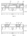
In Step 2010 of FIG. 20 and referring to FIG. 9, there is provided a semiconductor substrate 200 having a first region 201 and a second region 202. A second silicon oxide layer 215 can be formed on the semiconductor substrate 200. A first dummy gate 211 can be formed on the second silicon oxide layer 215 in the first region 201. A second dummy gate 212 can be formed on the second silicon oxide layer 215 in the second region 202. A first source region 221 and first drain region 222 can be formed in the semiconductor substrate 200 on both sides of the first dummy gate 211. A second source region 223 and second drain region 224 can be formed in the semiconductor substrate 200 on both sides of the second dummy gate 212.
An NMOS transistor can be formed in the first region 201, and a PMOS transistor can be formed in the second region 202, or vice versa. In one embodiment, the first source region 221 and the first drain region 222 can be N-type doped regions, and the second source region 223 and the second drain region 224 can be P-type doped regions.
In Step 2020 of FIG. 20 and referring to FIG. 10, an etch stop layer 235 can be formed on the semiconductor substrate 200 and on the first dummy gate 211 and the second dummy gate 212. An interlayer dielectric layer 230 can be formed on the etch stop layer 235. A polishing or planarization process, e.g., a CMP, can be performed to expose top surfaces of each of the first dummy gate 211 and the second dummy gate 212 from the interlayer dielectric layer 230. Further, the surface of the interlayer dielectric layer 230 can be flush with the surfaces of the first dummy gate 211 and the second dummy gate 212.
In Step 2030 of FIG. 20 and referring to FIG. 11, the first dummy gate 211 can be removed to form a first trench 241 in the first region 201. The second dummy gate 212 can be removed to form a second trench 242 in the second region 202.
In Step 2040 of FIG. 20 and referring to FIG. 12, a high-k gate dielectric layer 250 can be conformally formed on the entire surface of the structure shown in FIG. 11, including each surface of the bottoms and sidewalls of the first trench 241 and the second trench 242 and the interlayer dielectric layer 230.
In Step 2050 of FIG. 20 and referring to FIG. 13, the high-k gate dielectric layer 250 and/or related layers/components can be treated by a fluorination process. The fluorination process can include those disclosed above as shown in FIG. 5 and/or in Step 1950 in FIG. 19.
In Step 2060 of FIG. 20 and referring to FIG. 14, a functional layer can be formed on the fluorinated high-k gate dielectric layer 250. The functional layer can be partially etched, either in the first region 201 or in the second region 202 such that a first functional layer 261 formed in the first region 201 and a second functional layer 262 formed in the second region 202 can have different thickness. The difference in thickness may result in difference in work function for the two functional layers 261/262.
In a CMOS transistor, an NMOS transistor and a PMOS transistor may require their functional layers for different work functions by having different thicknesses and/or using different materials. For example, to form the structure shown in FIG. 14, a uniform functional layer can be formed first, and then a mask layer can be formed on the functional layer in the first region 201. The functional layer in the second region 202 can be partially etched using the mask layer such that the first functional layer 261 in the first region 201 and the second functional layer 262 in the second region 202 can have different thicknesses and thus different work functions. In this case, the processing time can be saved.
In other embodiments, the first and the second functional layers 261/262 can be formed on the fluorinated high-k gate dielectric layer in corresponding first and second regions by separate processes or steps.
In Step 2070 of FIG. 20 and referring to FIG. 15, a metal layer 270 can be formed on the first functional layer 261 and the second functional layer 262. The metal layer 270 can fill the first trench 241 in the first functional layer 261 in the first region 201 and can fill the second trench 242 in the second functional layer 262 in the second region 202.
In Step 2080 of FIG. 20 and referring to FIG. 16, the layers on the interlayer dielectric layer 230, including the metal layer 270, the first functional layer 261, the second functional layer 262, and the fluorinated high-k gate dielectric layer 250, can be polished to expose a surface of the interlayer dielectric layer 230. The metal layer 270 in the first trench, the first functional layer 261, and the fluorinated high-k dielectric layer 250 can form a first metal gate structure. The metal layer 270 in the second trench, the second functional layer 262, and the fluorinated high-k dielectric layer 250 can form a second metal gate structure.
In this manner, a metal gate structure can be formed by a process including, e.g., removing a dummy gate to form a trench; conformally forming a high-k gate dielectric layer on surfaces of the bottom and sidewall of the trench; and treating the high-k gate dielectric layer by a fluorination process such that fluorine bonds (e.g., F—Si, F—Hf, etc.) are formed between the high-k gate dielectric layer and the semiconductor substrate.
Since the fluorine bond can have higher bond energy than hydrogen bonds, the negative bias temperature instability of the formed transistor can be reduced. In addition, because fluorine is a strong oxidant, it can prevent oxygen vacancies from producing donor levels in the band gaps and from becoming positively charged. As a result, the oxygen vacancies can be passivated and the positive bias temperature instability of the formed devices can be reduced.
The embodiments disclosed herein are exemplary only. Other applications, advantages, alternations, modifications, or equivalents to the disclosed embodiments are obvious to those skilled in the art and are intended to be included within the scope of the present disclosure.

Claims (20)

What is claimed is:
1. A method for forming a transistor comprising:
providing a semiconductor substrate;
forming a dummy gate and an interlayer dielectric layer having a flushed top surface over the semiconductor substrate;
removing the dummy gate to form a trench over the semiconductor substrate;
forming a high-k dielectric layer over each surface of the trench and the interlayer dielectric layer;
fluorinating the high-k dielectric layer to form a fluorinated high-k dielectric layer by a fluorination process, wherein a channel region in the semiconductor substrate under the dummy gate is simultaneously fluorinated in the fluorination process;
forming a functional layer on the fluorinated high-k dielectric layer;
forming a metal layer on the functional layer to fill the trench with the metal layer; and
exposing the interlayer dielectric layer by polishing the metal layer, the functional layer, and the fluorinated high-k dielectric layer on the interlayer dielectric layer.
2. The method of claim 1, wherein the fluorinating includes one or more processes selected from an ion implantation with fluorine-containing ions, an annealing at a fluorine-containing atmosphere, and an annealing at a fluorine-containing plasma environment.
3. The method of claim 2, wherein the ion implantation with fluorine-containing ions includes:
plasma ionizing a fluorine-containing gas to form a fluorine-containing plasma; and
implanting the fluorine-containing plasma into the high-k dielectric layer using an implantation energy ranging from about 2 KeV to about 20 KeV and an implantation dosage ranging from about 1×10¹⁷ atoms/m3 to about 1×10²⁰ atoms/m3.
4. The method of claim 2, wherein the annealing at the fluorine-containing atmosphere includes controlling a reaction chamber to have a pressure ranging from about 0.5 Torr to about 5 Torr, a temperature ranging from about 300° C. to about 800° C., and an annealing time ranging from 5 seconds to about 60 seconds.
5. The method of claim 2, wherein the annealing at the fluorine-containing plasma environment includes:
forming a fluorine-containing plasma in a reaction chamber; and
controlling the reaction chamber to have a pressure ranging from about 0.5 Torr to about 5 Torr, a temperature ranging from about 300° C. to about 800° C., and an annealing time ranging about from about 5 seconds to about 60 seconds.
6. The method of claim 1, wherein the fluorinating uses a fluorine source selected from F2, HF, NF3, PF5, PF3, CF4, CH2F2, CHF3, or combinations thereof.
7. The method of claim 1, wherein the high-k dielectric layer is made of a material including HfO2, La2O3, HfSiON, HfAlO2, or combinations thereof.
8. The method of claim 1, wherein the functional layer is made of a material including Ti, Ta, TiN, TaN, TiAl, TaC, TaSiN, TiAlN, or combinations thereof.
9. The method of claim 1, further including:
conformally forming a first silicon oxide layer over each surface of the trench and the interlayer dielectric layer, and
forming the high-k dielectric layer over the first silicon oxide layer, wherein the first silicon oxide layer is fluorinated in the fluorination process.
10. The method of claim 1, wherein a second silicon oxide layer is formed between the semiconductor substrate and the dummy gate.
11. The method of claim 1, further including forming a source region and a drain region in the semiconductor substrate on both sides of the dummy gate.
12. The method of claim 1, further including:
forming a silicon oxide layer between the dummy gate and the semiconductor layer, wherein the silicon oxide layer is fluorinated in the fluorination process.
13. The method of claim 1, further including:
forming an etch stop layer between the interlayer dielectric layer and the semiconductor substrate and between the interlayer dielectric layer and the dummy gate, wherein the etch stop layer is capable of exerting a tensile or compressive stress on the semiconductor substrate.
14. A method for forming a CMOS transistor comprising:
providing a semiconductor substrate including a first region and a second region;
forming a first dummy gate in the first region and forming a second dummy gate in the second region;
forming an interlayer dielectric layer over the semiconductor substrate, wherein the interlayer dielectric layer has a top surface flushed with a top surface of each of the first and the second dummy gates;
removing the first dummy gate to form a first trench, and removing the second dummy gate to form a second trench;
conformally forming a high-k dielectric layer over each surface of the first trench, the second trench, and the interlayer dielectric layer;
simultaneously fluorinating the high-k dielectric layer in the first region and in the second region to form a fluorinated high-k dielectric layer by a fluorination process;
forming a first functional layer on the fluorinated high-k dielectric layer in the first region and forming a second functional layer on the fluorinated high-k dielectric layer in the second region, wherein the first functional layer and the second functional layer have different work functions;
forming a metal layer on the first and second functional layers to fill each of the first trench and the second trench; and
exposing the interlayer dielectric layer by a surface planarization process.
15. The method of claim 14, wherein forming the first functional layer and the second functional layer includes:
forming a functional layer on the fluorinated high-k dielectric layer in the first and second regions, and
partially etching the functional layer in one of the first and the second regions to form the first functional layer in the first region and the second functional layer in the second region, wherein the first and second functional layers have different thickness.
16. The method of claim 14, further including:
forming a source region and a drain region in the semiconductor substrate on both sides of the first dummy gate, and
forming a source region and a drain region in the semiconductor substrate on both sides of the second dummy gate.
17. The method of claim 14, wherein the surface planarization process includes polishing the metal layer, the first and second functional layers, and the fluorinated high-k dielectric layer on the interlayer dielectric layer.
18. The method of claim 14, wherein a channel region in the semiconductor substrate under each of the first dummy gate and the second dummy gate is simultaneously fluorinated in the fluorination process.
19. The method of claim 14, further including:
forming a silicon oxide layer under the first dummy gate and the second dummy gate, on the semiconductor layer, wherein the silicon oxide layer is fluorinated in the fluorination process.
20. The method of claim 14, further including:
forming an etch stop layer between the interlayer dielectric layer and the semiconductor substrate in the first and second regions, and between the interlayer dielectric layer and the first dummy gate, and between the interlayer dielectric layer and the second dummy gate, wherein the etch stop layer is capable of exerting a tensile or compressive stress on the semiconductor substrate.
US13/904,341 2012-09-18 2013-05-29 Transistor device and fabrication method Active 2034-01-01 US9147614B2 (en)

Applications Claiming Priority (3)

Application Number Priority Date Filing Date Title
CN201210348153 2012-09-18
CN201210348153.6 2012-09-18
CN201210348153.6A CN103681276B (en) 2012-09-18 2012-09-18 Metal gates, MOS transistor and CMOS structure forming method respectively

Publications (2)

Publication Number Publication Date
US20140077313A1 US20140077313A1 (en) 2014-03-20
US9147614B2 true US9147614B2 (en) 2015-09-29

Family

ID=50273602

Family Applications (1)

Application Number Title Priority Date Filing Date
US13/904,341 Active 2034-01-01 US9147614B2 (en) 2012-09-18 2013-05-29 Transistor device and fabrication method

Country Status (2)

Country Link
US (1) US9147614B2 (en)
CN (1) CN103681276B (en)

Families Citing this family (36)

* Cited by examiner, † Cited by third party
Publication number Priority date Publication date Assignee Title
US9219120B2 (en) * 2013-10-15 2015-12-22 Taiwan Semiconductor Manufacturing Company, Ltd. Semiconductor film with adhesion layer and method for forming the same
US9202809B2 (en) * 2014-02-06 2015-12-01 Taiwan Semiconductor Manufacturing Co., Ltd. Semiconductor device and method for manufacturing thereof
KR101536174B1 (en) * 2014-02-11 2015-07-14 연세대학교 산학협력단 Method of manufacturing semiconductor device capable of suppressing oxygen diffusion
US9472465B2 (en) * 2014-05-06 2016-10-18 GlobalFoundries, Inc. Methods of fabricating integrated circuits
CN105226023A (en) * 2014-06-26 2016-01-06 中芯国际集成电路制造(上海)有限公司 The formation method of semiconductor device
CN105990097B (en) * 2015-02-15 2020-03-27 盛美半导体设备(上海)股份有限公司 Polishing method of high-K dielectric silicon wafer
US9583584B2 (en) * 2015-07-10 2017-02-28 GlobalFoundries, Inc. Methods for producing integrated circuits using long and short regions and integrated circuits produced from such methods
CN106711034B (en) * 2015-08-31 2020-05-08 中芯国际集成电路制造(上海)有限公司 Method for forming semiconductor structure
US9978601B2 (en) * 2015-10-20 2018-05-22 Taiwan Semiconductor Manufacturing Co., Ltd. Methods for pre-deposition treatment of a work-function metal layer
US9502307B1 (en) 2015-11-20 2016-11-22 International Business Machines Corporation Forming a semiconductor structure for reduced negative bias temperature instability
US9837487B2 (en) * 2015-11-30 2017-12-05 Taiwan Semiconductor Manufacturing Co., Ltd. Structure and formation method of semiconductor device structure with gate stack
US9768171B2 (en) 2015-12-16 2017-09-19 International Business Machines Corporation Method to form dual tin layers as pFET work metal stack
CN107170683A (en) * 2016-03-08 2017-09-15 中芯国际集成电路制造(上海)有限公司 The forming method of fin formula field effect transistor
CN107564863B (en) * 2016-06-30 2020-10-16 中芯国际集成电路制造(上海)有限公司 Semiconductor device and manufacturing method thereof
CN107591437B (en) * 2016-07-07 2020-03-10 中芯国际集成电路制造(上海)有限公司 Method for forming semiconductor device
US20180033619A1 (en) * 2016-07-29 2018-02-01 Applied Materials, Inc. Performing decoupled plasma fluorination to reduce interfacial defects in film stack
CN107919283A (en) * 2016-10-10 2018-04-17 中芯国际集成电路制造(上海)有限公司 The forming method of fin field effect pipe
US10134873B2 (en) * 2016-11-18 2018-11-20 Taiwan Semiconductor Manufacturing Co., Ltd. Semiconductor device gate structure and method of fabricating thereof
CN108630521B (en) * 2017-03-17 2020-11-03 中芯国际集成电路制造(上海)有限公司 Method for manufacturing semiconductor device
CN109037334A (en) * 2017-06-12 2018-12-18 中芯国际集成电路制造(上海)有限公司 A kind of manufacturing method of semiconductor devices
US10276690B2 (en) * 2017-07-31 2019-04-30 Taiwan Semiconductor Manufacturing Company, Ltd. Semiconductor device and method
US10854459B2 (en) * 2017-09-28 2020-12-01 Taiwan Semiconductor Manufacturing Co., Ltd. Gate structure passivating species drive-in method and structure formed thereby
US10522344B2 (en) * 2017-11-06 2019-12-31 Taiwan Semiconductor Manufacturing Co., Ltd. Integrated circuits with doped gate dielectrics
CN110400746B (en) * 2018-04-24 2022-01-11 中芯国际集成电路制造(上海)有限公司 Semiconductor structure and forming method thereof
CN108682652B (en) * 2018-05-21 2021-02-02 上海华力集成电路制造有限公司 Method for manufacturing metal gate
US10672910B2 (en) 2018-08-09 2020-06-02 International Business Machines Corporation Threshold voltage adjustment from oxygen vacancy by scavenge metal filling at gate cut (CT)
US11088029B2 (en) * 2018-09-26 2021-08-10 Taiwan Semiconductor Manufacturing Co., Ltd. Gate stack treatment
KR20210011748A (en) * 2019-07-23 2021-02-02 삼성전자주식회사 A semiconductor device
CN110444472B (en) * 2019-08-27 2021-10-15 上海华力集成电路制造有限公司 Si-based Mosfet device and preparation method thereof
CN112563127B (en) * 2019-09-26 2023-10-31 中芯国际集成电路制造(上海)有限公司 Semiconductor device and method of forming the same
US11127838B2 (en) * 2019-11-05 2021-09-21 United Microelectronics Corp. Method of fabricating metal gate transistor
CN113628961A (en) * 2020-05-07 2021-11-09 中芯国际集成电路制造(上海)有限公司 Method for forming semiconductor device
CN113707547A (en) * 2020-05-22 2021-11-26 中芯国际集成电路制造(上海)有限公司 Method for forming semiconductor structure
CN112201582A (en) * 2020-09-30 2021-01-08 上海华力集成电路制造有限公司 Method for adjusting threshold voltage of MOS device
CN113257734B (en) * 2021-04-30 2023-06-23 北海惠科半导体科技有限公司 Semiconductor device, manufacturing method thereof and chip
US20230066477A1 (en) * 2021-08-31 2023-03-02 Taiwan Semiconductor Manufacturing Co., Ltd. Gate structures in transistors and method of forming same

Citations (3)

* Cited by examiner, † Cited by third party
Publication number Priority date Publication date Assignee Title
US20120080756A1 (en) * 2009-07-01 2012-04-05 Panasonic Corporation Semiconductor device and method for fabricating the same
US20120261758A1 (en) * 2011-04-14 2012-10-18 Taiwan Semiconductor Manufacturing Company, Ltd. Method of fabricating a gate dielectric layer
US20130062704A1 (en) * 2011-09-08 2013-03-14 International Business Machines Corporation Cmos structure having multiple threshold voltage devices

Family Cites Families (7)

* Cited by examiner, † Cited by third party
Publication number Priority date Publication date Assignee Title
JP4622318B2 (en) * 2004-06-04 2011-02-02 セイコーエプソン株式会社 Manufacturing method of semiconductor device
US7390709B2 (en) * 2004-09-08 2008-06-24 Intel Corporation Method for making a semiconductor device having a high-k gate dielectric layer and a metal gate electrode
US20080017936A1 (en) * 2006-06-29 2008-01-24 International Business Machines Corporation Semiconductor device structures (gate stacks) with charge compositions
CN102446767B (en) * 2010-10-12 2013-09-04 中芯国际集成电路制造(北京)有限公司 Manufacturing method of NMOS (N-channel metal oxide semiconductor) transistor
CN102479722B (en) * 2010-11-30 2014-03-12 中芯国际集成电路制造(北京)有限公司 Method for manufacturing transistor
CN102064111A (en) * 2010-12-06 2011-05-18 复旦大学 Method for releasing Fermi level pinning by utilizing plasma
CN102420117A (en) * 2011-06-07 2012-04-18 上海华力微电子有限公司 Method for improving negative bias temperature instability of gate-last positive channel metal oxide semiconductor (PMOS)

Patent Citations (3)

* Cited by examiner, † Cited by third party
Publication number Priority date Publication date Assignee Title
US20120080756A1 (en) * 2009-07-01 2012-04-05 Panasonic Corporation Semiconductor device and method for fabricating the same
US20120261758A1 (en) * 2011-04-14 2012-10-18 Taiwan Semiconductor Manufacturing Company, Ltd. Method of fabricating a gate dielectric layer
US20130062704A1 (en) * 2011-09-08 2013-03-14 International Business Machines Corporation Cmos structure having multiple threshold voltage devices

Also Published As

Publication number Publication date
CN103681276A (en) 2014-03-26
US20140077313A1 (en) 2014-03-20
CN103681276B (en) 2016-08-31

Similar Documents

Publication Publication Date Title
US9147614B2 (en) Transistor device and fabrication method
US9614051B2 (en) Semiconductor devices and fabrication method thereof
CN107958872B (en) Semiconductor device and method of forming the same
US8980705B2 (en) MOS transistors and fabrication method thereof
TWI388003B (en) Implantation method for reducing threshold voltage for high-k metal gate device
JP5427148B2 (en) Semiconductor device
TWI420652B (en) Method of forming a single metal that performs n and p work functions in high-k/metal gate devices
US10269659B2 (en) Semiconductor structure and fabrication method thereof
US9741819B2 (en) Transistor device and fabrication method
JP2004158487A (en) Method of manufacturing semiconductor device
JP2008300779A (en) Semiconductor device and manufacturing method therefor
WO2014082334A1 (en) Method for manufacturing semiconductor device
JP2008283182A (en) Method of manufacturing pmos transistor, and method of manufacturing cmos transistor
JP2012044013A (en) Manufacturing method of semiconductor device
US9934975B2 (en) N-type MOSFET and method for manufacturing the same
US20110227160A1 (en) Semiconductor Device and Method of Manufacturing the Same
CN107346783B (en) Semiconductor structure and manufacturing method thereof
US20140015063A1 (en) Method for Forming Gate Structure, Method for Forming Semiconductor Device, and Semiconductor Device
KR101347943B1 (en) Cmos devices with metal gates and methods for forming the same
CN103094214B (en) Manufacturing method for semiconductor device
JP2009252895A (en) Semiconductor device and method of manufacturing the same
CN108987248B (en) Semiconductor structure and forming method thereof
US9984882B2 (en) Semiconductor structures and fabrication method thereof
US20100123200A1 (en) Semiconductor device and method of manufacturing the same
CN109671673B (en) Semiconductor structure and forming method thereof

Legal Events

Date Code Title Description
AS Assignment

Owner name: SEMICONDUCTOR MANUFACTURING INTERNATIONAL CORP., C

Free format text: ASSIGNMENT OF ASSIGNORS INTEREST;ASSIGNORS:LI, AILEEN;NI, JINGHUA;REEL/FRAME:030503/0363

Effective date: 20130515

STCF Information on status: patent grant

Free format text: PATENTED CASE

MAFP Maintenance fee payment

Free format text: PAYMENT OF MAINTENANCE FEE, 4TH YEAR, LARGE ENTITY (ORIGINAL EVENT CODE: M1551); ENTITY STATUS OF PATENT OWNER: LARGE ENTITY

Year of fee payment: 4

MAFP Maintenance fee payment

Free format text: PAYMENT OF MAINTENANCE FEE, 8TH YEAR, LARGE ENTITY (ORIGINAL EVENT CODE: M1552); ENTITY STATUS OF PATENT OWNER: LARGE ENTITY

Year of fee payment: 8