JP2006032077A - Dc circuit breaker - Google Patents
Dc circuit breaker Download PDFInfo
- Publication number
- JP2006032077A JP2006032077A JP2004208126A JP2004208126A JP2006032077A JP 2006032077 A JP2006032077 A JP 2006032077A JP 2004208126 A JP2004208126 A JP 2004208126A JP 2004208126 A JP2004208126 A JP 2004208126A JP 2006032077 A JP2006032077 A JP 2006032077A
- Authority
- JP
- Japan
- Prior art keywords
- commutation
- circuit
- circuit breaker
- capacitor
- reactor
- Prior art date
- Legal status (The legal status is an assumption and is not a legal conclusion. Google has not performed a legal analysis and makes no representation as to the accuracy of the status listed.)
- Granted
Links
Images


Landscapes
- Driving Mechanisms And Operating Circuits Of Arc-Extinguishing High-Tension Switches (AREA)
Abstract
Description
本発明は、転流回路の耐電圧特性を改善し得る直流遮断器に関する。 The present invention relates to a DC circuit breaker that can improve the withstand voltage characteristics of a commutation circuit.
電気鉄道用き電回路のような直流回路においては、電源側に直流遮断器が設けられ、直流回路の事故電流や通電電流の開閉が行われている。 In a DC circuit such as a power circuit for an electric railway, a DC circuit breaker is provided on the power supply side to open and close an accident current and an energization current of the DC circuit.
従来の直流遮断器は、図7に示すように、直流回路の電源側(P)−負荷側(N)間に接離自在の一対の接点を有する主遮断器1と副遮断器2とが直列接続されている。主遮断器1には、転流コンデンサ3、リアクトル4および転流スイッチ5を有する転流回路6が並列接続されている。そして、転流スイッチ5が、転流コンデンサ3およびリアクトル4よりも負荷側に接続されている。また、主遮断器1が遮断後に発生する電磁エネルギーを吸収するためサージアブソーバ7が並列接続されている。
As shown in FIG. 7, the conventional DC circuit breaker includes a
このような回路構成において、直流回路に事故電流が流れた場合、転流スイッチ5が閉じられ、主遮断器1に転流回路6から振動性の転流電流を注入して事故電流を遮断し、次いで副遮断器2で直流回路を開路するようになっている。
In such a circuit configuration, when an accidental current flows through the DC circuit, the
この場合、転流コンデンサ3は、負荷側が正極性に充電されているので、転流電流は、転流コンデンサ3→リアクトル4→転流スイッチ5→主遮断器1→転流コンデンサ3で形成される閉回路を流れる。そして、事故電流の向きと逆方向の転流電流により零点が形成され、主遮断器1で容易に遮断できるようになっている(例えば、特許文献1参照。)。
上記の従来の直流遮断器においては、次のような問題がある。
主遮断器1と副遮断器2とを閉極すると、直流回路には運転電圧V0が印加される。即ち、主遮断器1および副遮断器2は対地電位V0の電位となる。この場合、転流スイッチ5は開路されており、また、転流コンデンサ3は予め所定の充電電圧Vcに充電された状態にある。
The above conventional DC circuit breaker has the following problems.
When the
そして、転流回路6を構成する機器のうち、リアクトル4、リアクトル4と接続されている転流コンデンサ3の一方の端子、およびリアクトル4と接続されている転流スイッチ5の一方の端子のそれぞれの対地間には、運転電圧V0と充電電圧Vcとが同極性のため、これらを加算した電圧Vx(=V0+Vc)が加わることになる。したがって、これらの機器の対地間絶縁は、電圧Vxに耐え得る耐電圧性能を必要とする。
Of the devices constituting the
このように高い耐電圧性能を得るためには、例えばリアクトル4の対地間の絶縁構造や転流コンデンサ3の端子を構成する対地間絶縁のブッシングなどを大型化しなければならず、転流回路6を構成する機器に加わる電圧の低減が望まれていた。
In order to obtain such a high withstand voltage performance, for example, the insulation structure between the ground of the
本発明は上記問題を解決するためになされたもので、転流回路に加わる電圧を低減し、耐電圧性能を改善し得る直流遮断器を得ることを目的とする。 The present invention has been made to solve the above problems, and an object of the present invention is to obtain a DC circuit breaker that can reduce the voltage applied to the commutation circuit and improve the withstand voltage performance.
上記目的を達成するために、直流電流を遮断する主遮断器と、この主遮断器に直列に接続された副遮断器と、直列に接続した転流スイッチ、リアクトル、および転流コンデンサを有し前記主遮断器に並列に接続された転流回路と、前記転流回路の前記転流コンデンサを充電する充電回路とを備え、電源側と負荷側の間に設置される直流遮断器において、前記リアクトルおよび前記転流コンデンサが前記転流スイッチよりも負荷側に接続されていることを特徴とする。 In order to achieve the above object, a main circuit breaker for cutting off a direct current, a sub circuit breaker connected in series to the main circuit breaker, a commutation switch, a reactor, and a commutation capacitor connected in series are provided. In a DC circuit breaker installed between a power supply side and a load side, comprising a commutation circuit connected in parallel to the main circuit breaker, and a charging circuit for charging the commutation capacitor of the commutation circuit, The reactor and the commutation capacitor are connected to a load side from the commutation switch.
本発明によれば、直流遮断器の転流回路において、所定の電圧で充電された転流コンデンサの充電電圧と直流回路の運転電圧とが加算されないようにしているので、転流回路を構成する機器の対地間に加わる電位差が抑制され、これらの機器を低減した絶縁とすることができる。 According to the present invention, in the commutation circuit of the DC circuit breaker, the commutation circuit is configured because the charging voltage of the commutation capacitor charged with a predetermined voltage and the operation voltage of the DC circuit are not added. The potential difference applied between the grounds of the devices is suppressed, and these devices can be reduced in insulation.
以下、本発明による直流遮断器を図面を参照して説明する。 Hereinafter, a DC circuit breaker according to the present invention will be described with reference to the drawings.
先ず、本発明の実施例1に係る直流遮断器を図1を参照して説明する。図1は、本発明の実施例1に係る直流遮断器の回路構成図である。なお、図1において、従来と同様の構成部分については、同一符号を付した。
First, a DC circuit breaker according to
図1に示すように、直流回路の電源側(P)−負荷側(N)間には、接離自在の一対の接点を有する真空バルブからなる主遮断器1と副遮断器2とが直列接続されている。主遮断器1には、転流スイッチ5、リアクトル4および転流コンデンサ3を有する転流回路6が並列接続されている。この転流回路6には、転流スイッチ5、リアクトル4および転流コンデンサ3が、この順序で直列接続され、転流コンデンサ3が負荷側に設けられている。また、この主遮断器1が遮断後に発生する電磁エネルギーを吸収するためサージアブソーバ7が並列接続されている。
As shown in FIG. 1, a
また、転流コンデンサ3の端子間には、充電回路10が接続され、直流回路の電圧(主遮断器1の対地電位)が正極性の場合、副遮断器2側の端子が同極性の正極性に充電されている。この充電回路10には、直列接続された第1の保護抵抗11、第1の充電スイッチ12および第1のダイオード13と、同様に直列接続された第2の保護抵抗14、第2の充電スイッチ15および第1のダイオード13と電流の向きが逆向きの第2のダイオード16とが並列接続され、電源17に接続されている。また、直流回路に接続された極性判別器18により、第1の充電スイッチ12または第2の充電スイッチ15が動作するようになっている。
In addition, when the
そして、直流回路に事故電流が流れた場合、図示しない制御回路からの信号により、主遮断器1が開極を始め、主遮断器1の転流動作位置に達すると、図示しない制御回路からの信号により、転流スイッチ5が閉じられ、事故電流に転流回路6からの振動性の転流電流を重畳して主遮断器1で事故電流を遮断し、次いで副遮断器2で直流回路を開路するようになっている。この場合、転流コンデンサ3は、負荷側の端子が正極性に充電されているので、転流電流は、転流コンデンサ3→主遮断器1→転流スイッチ5→リアクトル4→転流コンデンサ3で形成される閉回路を流れる。そして、事故電流の向きと逆方向の転流電流により、零点が形成され、主遮断器1で遮断できるようになっている。
When an accidental current flows in the DC circuit, the
ここで、転流コンデンサ3の充電においては、主遮断器1の対地電位の極性を極性判別器18で検出し、例えば主遮断器1の対地電位が正極性であれば、第1の充電スイッチ12を閉路して、転流コンデンサ3の負荷側の端子が正極性に充電されるようになっている。逆に、主遮断器1の対地電位が負極性であれば、第2の充電スイッチ15が閉路され、転流コンデンサ3の負荷側の端子が負極性に充電されるようになっている。
Here, in the charging of the
このような極性で所定の電圧Vcに充電された転流コンデンサ3において、主遮断器1と副遮断器2とを閉極して、直流回路に運転電圧V0を印加したときの転流回路6の電位差を説明する。
In the
転流回路6を構成する機器のうち、リアクトル4と接続されている転流コンデンサ3の一方の端子から、リアクトル4、およびリアクトル4と接続されている転流スイッチ5の一方の端子までの間のそれぞれの対地間には、主遮断器1の対地電位がV0となるため、運転電圧V0から充電電圧Vcを減算した電圧Vz(=V0−Vc)が加わることになる。即ち、例えば主遮断器1の対地電位の極性が正極性であれば、リアクトル4と接続されている転流コンデンサ3の一方の端子から、リアクトル4、およびリアクトル4と接続されている転流スイッチ5の一方の端子までの間は、負極性となるので、これらの機器の対地間に加わる電位差は減算されることになる。
Among the devices composing the
この電圧Vzは、運転電圧V0と充電電圧Vcを加算した電圧Vxよりも低くなる。このため、これらの機器の対地間絶縁は、電圧Vzに耐え得る耐電圧性能でよく、低減した絶縁とすることができる。 This voltage Vz is lower than the voltage Vx obtained by adding the operating voltage V0 and the charging voltage Vc. For this reason, the ground-to-ground insulation of these devices may be a withstand voltage performance that can withstand the voltage Vz, and can be reduced insulation.
上記実施例1の直流遮断器によれば、転流回路6を転流スイッチ5、リアクトル4および転流コンデンサ3の順序で直列接続し、転流コンデンサ3を負荷側に設けるともに、転流コンデンサ3の負荷側の端子を直流回路の極性と同極性に充電しているので、リアクトル4と接続されている転流コンデンサ3の一方の端子から、リアクトル4、およびリアクトル4と接続されている転流スイッチ5の一方の端子までの間のこれらの対地間に加わる電位差を抑制でき、これらの機器を低減した絶縁とすることができる。
According to the DC circuit breaker of the first embodiment, the
次に、本発明の実施例2に係る直流遮断器を図2を参照して説明する。図2は、本発明の実施例2に係る直流遮断器の転流回路の回路構成図である。なお、この実施例2が実施例1と異なる点は、転流回路の構成である。図2において、実施例1と同様の構成部分においては、同一符号を付し、その詳細な説明を省略する。
Next, a DC circuit breaker according to
図2に示すように、転流回路6には、リアクトル4、転流スイッチ5および転流コンデンサ3が、この順序で直列接続され、副遮断器2側に転流コンデンサ3が設けられている。また、転流コンデンサ3の副遮断器2側の端子には、直流回路の極性と同極性の所定の電圧Vcが充電されている。
As shown in FIG. 2, a
このような極性で充電された転流コンデンサ3において、主遮断器1と副遮断器2とを閉極して、直流回路に運転電圧V0を印加したときの転流回路6の電位差を説明する。
In the
転流回路6を構成する機器のうち、転流コンデンサ3と転流スイッチ5とを接続しているそれぞれの端子間の対地間には、運転電圧V0と充電電圧Vcとを減算した電圧Vz(=V0−Vc)が加わることになる。即ち、例えば主遮断器1の対地電位の極性が正極性であれば、転流コンデンサ3の一方の端子と転流スイッチ5の一方の端子間は、負極性となっているので、これらの対地間に加わる電位差は減算されることになる。
Among the devices composing the
上記実施例2の直流遮断器によれば、転流回路6の機器を、リアクトル4、転流スイッチ5、および転流コンデンサ3の順序で直列接続し、転流コンデンサ3を負荷側に設け、転流コンデンサ3の負荷側の端子を主遮断器1の対地電位の極性と同極性の電圧で充電しているので、転流コンデンサ3と転流スイッチ5とを接続しているそれぞれの端子間に加わる電位差を抑制でき、これらの機器を低減した絶縁とすることができる。
According to the DC circuit breaker of the second embodiment, the
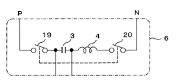
次に、本発明の実施例3に係る直流遮断器を図3を参照して説明する。図3は、本発明の実施例3に係る直流遮断器の転流回路の回路構成図である。なお、この実施例3が実施例1と異なる点は、転流回路の構成である。図3において、実施例1と同様の構成部分においては、同一符号を付し、その詳細な説明を省略する。
Next, a DC circuit breaker according to
図3に示すように、転流回路6には、第1の転流スイッチ19、転流コンデンサ3、リアクトル4、および第2の転流スイッチ20の順序で、これらが直列接続されている。ここで、転流コンデンサ3とリアクトル4との順序は入れ替わってもよい。また、第1の転流スイッチ19と第2の転流スイッチ20とは、連動して開閉されるようになっている。
As shown in FIG. 3, the
そして、主遮断器1と副遮断器2とを閉極して、直流回路に運転電圧V0を印加したときの転流回路6の電位差を説明する。
Then, the potential difference of the
第1の転流スイッチ19の一方の端子から転流コンデンサ3の一方の端子までの機器と、第2の転流スイッチ20の一方の端子からリアクトル4を介して転流コンデンサ3の他方の端子までの機器との対地間の静電容量を同様とすれば、転流コンデンサ3の対地間には、転流コンデンサ3を所定の電圧Vcで充電した時、1/2Vc(=対地間電圧Vc1)が加わる。
A device from one terminal of the
そして、転流コンデンサ3が充電される極性によって、これらの機器の対地間には、対地間電圧Vc1が加算、もしくは減算された電圧Vz1(=V0±Vc1)が加わることになる。即ち、転流コンデンサ3の負荷側の端子が、直流回路と同極性であれば減算した電圧になり、異極性であれば加算した電圧になる。この電圧Vz1は、運転電圧V0と充電電圧Vcとを加算した電圧Vxよりも低くなる。
Then, depending on the polarity with which the
上記実施例3の直流遮断器によれば、第1の転流スイッチ19と第2の転流スイッチ20間に、転流コンデンサ3とリアクトル4とを接続しているので、転流コンデンサ3とリアクトル4との対地間に加わる電位差を抑制でき、これらの機器を低減した絶縁とすることができる。
According to the DC circuit breaker of the third embodiment, the
次に、本発明の実施例4に係る直流遮断器を図4を参照して説明する。図4は、本発明の実施例4に係る直流遮断器の転流回路の回路構成図である。なお、この実施例4が実施例1と異なる点は、転流回路の構成である。図4において、実施例1と同様の構成部分においては、同一符号を付し、その詳細な説明を省略する。
Next, a DC circuit breaker according to
図4に示すように、転流回路6には、転流スイッチ5、副リアクトル21、副転流コンデンサ22、リアクトル4および転流コンデンサ3の順序で、これらが直列接続され、転流コンデンサ3が負荷側に設けられている。また、副リアクトル21と副転流コンデンサ22とには、切替スイッチ23が並列接続されている。これは、転流電流を制御するためのものであり、切替スイッチ23を閉路すれば転流電流を増大することができ、また、開路すれば抑制することができる。
As shown in FIG. 4, the
上記実施例4の直流遮断器によれば、副リアクトル21や副転流コンデンサ22などを接続し、転流電流を制御する転流回路6においても、実施例1と同様の効果を得ることができる。
According to the DC circuit breaker of the fourth embodiment, the same effect as that of the first embodiment can be obtained also in the
なお、上記実施例4では、実施例1の転流回路6に副リアクトル21と副転流コンデンサ22とを直列接続して説明したが、実施例2および実施例3の転流回路6においても、これらの副リアクトル21、副転流コンデンサ22および切替スイッチ23を接続してもよい。ここで、リアクトル4と副リアクトル21とを合わせて、単に転流回路6のリアクトル、また、転流コンデンサ3と副転流コンデンサ22とを合わせて、単に転流回路6の転流コンデンサと称す。
In the fourth embodiment, the
次に、本発明の実施例5に係る直流遮断器を図5を参照して説明する。図5は、本発明の実施例5に係る直流遮断器の転流回路の回路構成図である。なお、この実施例5が実施例1と異なる点は、転流回路の構成である。図5において、実施例1と同様の構成部分においては、同一符号を付し、その詳細な説明を省略する。
Next, a DC circuit breaker according to
図5に示すように、転流回路6には、転流スイッチ5、副リアクトル21、副転流コンデンサ22、リアクトル4および転流コンデンサ3の順序で、これらが直列接続され、転流コンデンサ3が負荷側に設けられている。また、副リアクトル21には、切替スイッチ24が並列接続されている。これは、転流電流を制御するためのものであり、切替スイッチ24を閉路すれば転流電流を増大することができ、また、開路すれば抑制することができる。
As shown in FIG. 5, the
上記実施例5の直流遮断器によれば、副リアクトル21や副転流コンデンサ22などを接続し、転流電流を制御する転流回路6においても、実施例1と同様の効果を得ることができる。
According to the DC circuit breaker of the fifth embodiment, the same effect as that of the first embodiment can be obtained also in the
なお、上記実施例5では、実施例1の転流回路6に副リアクトル21と副転流コンデンサ22とを直列接続して説明したが、実施例2および実施例3の転流回路6においても、これらの副リアクトル21、副転流コンデンサ22および切替スイッチ24を接続してもよい。ここで、リアクトル4と副リアクトル21とを合わせて、単に転流回路6のリアクトル、また、転流コンデンサ3と副転流コンデンサ22とを合わせて、単に転流回路6の転流コンデンサと称す。
In the fifth embodiment, the
次に、本発明の実施例6に係る直流遮断器を図6を参照して説明する。図6は、本発明の実施例6に係る直流遮断器の転流回路の回路構成図である。なお、この実施例6が実施例1と異なる点は、転流回路の構成である。図6において、実施例1と同様の構成部分においては、同一符号を付し、その詳細な説明を省略する。
Next, a DC circuit breaker according to
図6に示すように、転流回路6には、転流スイッチ5、副リアクトル21、副転流コンデンサ22、リアクトル4および転流コンデンサ3の順序で、これらが直列接続され、転流コンデンサ3が負荷側に設けられている。また、副転流コンデンサ22には、切替スイッチ25が並列接続されている。これは、転流電流を制御するためのものであり、切替スイッチ25を閉路すれば転流電流を増大することができ、また、開路すれば抑制することができる。
As shown in FIG. 6, the
上記実施例6の直流遮断器によれば、副リアクトル21や副転流コンデンサ22などを接続し、転流電流を制御する転流回路6においても、実施例1と同様の効果を得ることができる。
According to the DC circuit breaker of the sixth embodiment, the same effect as that of the first embodiment can be obtained also in the
なお、上記実施例6では、実施例1の転流回路6に副リアクトル21と副転流コンデンサ22とを直列接続して説明したが、実施例2および実施例3の転流回路6においても、これらの副リアクトル21、副転流コンデンサ22および切替スイッチ25を接続してもよい。ここで、リアクトル4と副リアクトル21とを合わせて、単に転流回路6のリアクトル、また、転流コンデンサ3と副転流コンデンサ22とを合わせて、単に転流回路6の転流コンデンサと称す。
In the sixth embodiment, the
1 主遮断器
2 副遮断器
3 転流コンデンサ
4 リアクトル
5 転流スイッチ
6 転流回路
7 サージアブソーバ
10 充電回路
11 第1の保護抵抗
12 第1の充電スイッチ
13 第1のダイオード
14 第2の保護抵抗
15 第2の充電スイッチ
16 第2のダイオード
17 電源
18 極性判別器
19 第1の転流スイッチ
20 第2の転流スイッチ
21 副リアクトル
22 副転流コンデンサ
23、24、25 切替スイッチ
DESCRIPTION OF
Claims (3)
この主遮断器に直列に接続された副遮断器と、
直列に接続した転流スイッチ、リアクトル、および転流コンデンサを有し前記主遮断器に並列に接続された転流回路と、
前記転流回路の前記転流コンデンサを充電する充電回路とを備え、電源側と負荷側の間に設置される直流遮断器において、
前記リアクトルおよび前記転流コンデンサが前記転流スイッチよりも負荷側に接続されていることを特徴とする直流遮断器。 A main circuit breaker that cuts off DC current;
A secondary circuit breaker connected in series to the main circuit breaker;
A commutation circuit having a commutation switch, a reactor, and a commutation capacitor connected in series and connected in parallel to the main circuit breaker;
A DC circuit breaker installed between the power supply side and the load side, comprising a charging circuit for charging the commutation capacitor of the commutation circuit;
The DC breaker, wherein the reactor and the commutation capacitor are connected to a load side of the commutation switch.
この主遮断器に直列に接続された副遮断器と、
直列に接続した第1の転流スイッチ、転流コンデンサ、リアクトルおよび第2の転流スイッチを有し前記主遮断器に並列に接続された転流回路と、
前記転流回路の前記転流コンデンサを充電する充電回路とを備え、
前記リアクトルおよび前記転流コンデンサは、前記第1の転流スイッチと前記第2の転流スイッチ間に接続され、前記第1の転流スイッチと前記第2の転流スイッチは連動して開閉することを特徴とする直流遮断器。 A main circuit breaker that cuts off DC current;
A secondary circuit breaker connected in series to the main circuit breaker;
A commutation circuit having a first commutation switch, a commutation capacitor, a reactor and a second commutation switch connected in series and connected in parallel to the main circuit breaker;
A charging circuit for charging the commutation capacitor of the commutation circuit,
The reactor and the commutation capacitor are connected between the first commutation switch and the second commutation switch, and the first commutation switch and the second commutation switch open and close in conjunction with each other. DC breaker characterized by that.
Priority Applications (1)
| Application Number | Priority Date | Filing Date | Title |
|---|---|---|---|
| JP2004208126A JP4660131B2 (en) | 2004-07-15 | 2004-07-15 | DC circuit breaker |
Applications Claiming Priority (1)
| Application Number | Priority Date | Filing Date | Title |
|---|---|---|---|
| JP2004208126A JP4660131B2 (en) | 2004-07-15 | 2004-07-15 | DC circuit breaker |
Publications (2)
| Publication Number | Publication Date |
|---|---|
| JP2006032077A true JP2006032077A (en) | 2006-02-02 |
| JP4660131B2 JP4660131B2 (en) | 2011-03-30 |
Family
ID=35898181
Family Applications (1)
| Application Number | Title | Priority Date | Filing Date |
|---|---|---|---|
| JP2004208126A Expired - Fee Related JP4660131B2 (en) | 2004-07-15 | 2004-07-15 | DC circuit breaker |
Country Status (1)
| Country | Link |
|---|---|
| JP (1) | JP4660131B2 (en) |
Cited By (17)
| Publication number | Priority date | Publication date | Assignee | Title |
|---|---|---|---|---|
| JP2009181908A (en) * | 2008-01-31 | 2009-08-13 | Toshiba Mitsubishi-Electric Industrial System Corp | Dc high-speed vacuum circuit breaker |
| JP2010287460A (en) * | 2009-06-12 | 2010-12-24 | Hitachi Ltd | Commutation type direct current breaker |
| DE102010052136A1 (en) * | 2010-11-22 | 2012-05-24 | Siemens Aktiengesellschaft | Circuit arrangements for electronically controlled DC networks |
| WO2013164874A1 (en) * | 2012-05-01 | 2013-11-07 | 三菱電機株式会社 | Dc circuit breaker |
| US8822862B2 (en) | 2009-06-30 | 2014-09-02 | Panasonic Corporation | DC breaker |
| CN104380421A (en) * | 2012-06-13 | 2015-02-25 | 西门子公司 | Apparatus for switching in dc voltage mains |
| JP2015043656A (en) * | 2013-08-26 | 2015-03-05 | 株式会社東芝 | Circuit breaker |
| WO2015166600A1 (en) * | 2014-05-01 | 2015-11-05 | 三菱電機株式会社 | Direct current shutoff device |
| JPWO2013164874A1 (en) * | 2012-05-01 | 2015-12-24 | 三菱電機株式会社 | DC circuit breaker |
| CN107565524A (en) * | 2017-09-30 | 2018-01-09 | 南方电网科学研究院有限责任公司 | Novel quick mechanical type high voltage direct current circuit breaker |
| US10063046B2 (en) | 2015-05-13 | 2018-08-28 | Lsis Co., Ltd. | Direct current circuit breaker and method using the same |
| US10184452B2 (en) | 2014-09-16 | 2019-01-22 | Mitsubishi Electric Corporation | Wind power generation system and DC power transmission system |
| US10403449B2 (en) | 2014-10-09 | 2019-09-03 | Mitsubishi Electric Corporation | Direct-current circuit breaker |
| JP6704539B1 (en) * | 2019-05-28 | 2020-06-03 | 三菱電機株式会社 | Breaker |
| CN112510647A (en) * | 2020-10-30 | 2021-03-16 | 西安交通大学 | Direct current breaker combining oscillation transfer and solid-state switch |
| WO2022116043A1 (en) * | 2020-12-02 | 2022-06-09 | Abb Schweiz Ag | Direct current circuit breaker and protection system |
| CN118017448A (en) * | 2024-04-10 | 2024-05-10 | 四川大学 | Inductance-variable mechanical direct current breaker |
Citations (6)
| Publication number | Priority date | Publication date | Assignee | Title |
|---|---|---|---|---|
| JPS5954132A (en) * | 1982-09-22 | 1984-03-28 | 株式会社日立製作所 | Dc breaker |
| JPS6065411A (en) * | 1983-09-21 | 1985-04-15 | 株式会社日立製作所 | Line charging type dc breaker |
| JP2001143581A (en) * | 1999-11-17 | 2001-05-25 | Hitachi Ltd | Shunt breaker of direct current |
| JP2001176363A (en) * | 1999-12-17 | 2001-06-29 | Fuji Electric Co Ltd | Direct-current breaker |
| JP2003264932A (en) * | 2002-03-08 | 2003-09-19 | Osaka Gas Co Ltd | High-speed current limiting and interrupting device for electric power system interconnection |
| JP2003346612A (en) * | 2002-05-28 | 2003-12-05 | Mitsubishi Electric Corp | Switching device |
-
2004
- 2004-07-15 JP JP2004208126A patent/JP4660131B2/en not_active Expired - Fee Related
Patent Citations (6)
| Publication number | Priority date | Publication date | Assignee | Title |
|---|---|---|---|---|
| JPS5954132A (en) * | 1982-09-22 | 1984-03-28 | 株式会社日立製作所 | Dc breaker |
| JPS6065411A (en) * | 1983-09-21 | 1985-04-15 | 株式会社日立製作所 | Line charging type dc breaker |
| JP2001143581A (en) * | 1999-11-17 | 2001-05-25 | Hitachi Ltd | Shunt breaker of direct current |
| JP2001176363A (en) * | 1999-12-17 | 2001-06-29 | Fuji Electric Co Ltd | Direct-current breaker |
| JP2003264932A (en) * | 2002-03-08 | 2003-09-19 | Osaka Gas Co Ltd | High-speed current limiting and interrupting device for electric power system interconnection |
| JP2003346612A (en) * | 2002-05-28 | 2003-12-05 | Mitsubishi Electric Corp | Switching device |
Cited By (22)
| Publication number | Priority date | Publication date | Assignee | Title |
|---|---|---|---|---|
| JP2009181908A (en) * | 2008-01-31 | 2009-08-13 | Toshiba Mitsubishi-Electric Industrial System Corp | Dc high-speed vacuum circuit breaker |
| JP2010287460A (en) * | 2009-06-12 | 2010-12-24 | Hitachi Ltd | Commutation type direct current breaker |
| US8822862B2 (en) | 2009-06-30 | 2014-09-02 | Panasonic Corporation | DC breaker |
| DE102010052136A1 (en) * | 2010-11-22 | 2012-05-24 | Siemens Aktiengesellschaft | Circuit arrangements for electronically controlled DC networks |
| US9515483B2 (en) | 2010-11-22 | 2016-12-06 | Siemens Aktiengesellschaft | Circuit arrangements for electronically controlled DC grids |
| WO2013164874A1 (en) * | 2012-05-01 | 2013-11-07 | 三菱電機株式会社 | Dc circuit breaker |
| JPWO2013164874A1 (en) * | 2012-05-01 | 2015-12-24 | 三菱電機株式会社 | DC circuit breaker |
| CN104380421A (en) * | 2012-06-13 | 2015-02-25 | 西门子公司 | Apparatus for switching in dc voltage mains |
| US10141732B2 (en) | 2012-06-13 | 2018-11-27 | Siemens Aktiengesellschaft | Apparatus for switching in a DC voltage grid |
| JP2015043656A (en) * | 2013-08-26 | 2015-03-05 | 株式会社東芝 | Circuit breaker |
| JP6042035B2 (en) * | 2014-05-01 | 2016-12-14 | 三菱電機株式会社 | DC breaker |
| WO2015166600A1 (en) * | 2014-05-01 | 2015-11-05 | 三菱電機株式会社 | Direct current shutoff device |
| US10184452B2 (en) | 2014-09-16 | 2019-01-22 | Mitsubishi Electric Corporation | Wind power generation system and DC power transmission system |
| US10403449B2 (en) | 2014-10-09 | 2019-09-03 | Mitsubishi Electric Corporation | Direct-current circuit breaker |
| US10063046B2 (en) | 2015-05-13 | 2018-08-28 | Lsis Co., Ltd. | Direct current circuit breaker and method using the same |
| CN107565524A (en) * | 2017-09-30 | 2018-01-09 | 南方电网科学研究院有限责任公司 | Novel quick mechanical type high voltage direct current circuit breaker |
| JP6704539B1 (en) * | 2019-05-28 | 2020-06-03 | 三菱電機株式会社 | Breaker |
| CN112510647A (en) * | 2020-10-30 | 2021-03-16 | 西安交通大学 | Direct current breaker combining oscillation transfer and solid-state switch |
| CN112510647B (en) * | 2020-10-30 | 2022-04-01 | 西安交通大学 | Direct current breaker combining oscillation transfer and solid-state switch |
| WO2022116043A1 (en) * | 2020-12-02 | 2022-06-09 | Abb Schweiz Ag | Direct current circuit breaker and protection system |
| CN118017448A (en) * | 2024-04-10 | 2024-05-10 | 四川大学 | Inductance-variable mechanical direct current breaker |
| CN118017448B (en) * | 2024-04-10 | 2024-06-18 | 四川大学 | Inductance-variable mechanical direct current breaker |
Also Published As
| Publication number | Publication date |
|---|---|
| JP4660131B2 (en) | 2011-03-30 |
Similar Documents
| Publication | Publication Date | Title |
|---|---|---|
| JP4660131B2 (en) | DC circuit breaker | |
| KR101521545B1 (en) | Device and method to interrupt high voltage direct current | |
| JP6049913B2 (en) | DC circuit breaker | |
| EP3200213B1 (en) | Direct current circuit breaker | |
| CN106663557B (en) | For interrupting the separating switch of DC current | |
| CN106099841A (en) | DC circuit-breaker and the method for use | |
| EP3035471A1 (en) | High voltage dc breaker | |
| US11075513B2 (en) | Circuit breaker | |
| WO2016185579A1 (en) | Power supply control device and power supply control method | |
| US10483072B2 (en) | Interrupter device for interrupting a direct current | |
| US10937612B2 (en) | DC voltage switch | |
| US5379014A (en) | Vacuum circuit breaker | |
| JPWO2015166600A1 (en) | DC breaker | |
| WO2018131307A1 (en) | Arc-suppressing device | |
| JP6202871B2 (en) | DC circuit breaker | |
| JP2010238391A (en) | Direct-current breaker | |
| JP2018125270A (en) | DC power system safety switchgear | |
| CN106328439A (en) | Relay module | |
| JP2006260925A (en) | Direct current high speed vacuum circuit breaker | |
| US20240305086A1 (en) | Dc solid-state circuit breaker with a solid-state aided airgap that provides a fail-safe mechanism | |
| JP2002110006A (en) | Direct current breaker | |
| JP2005044591A (en) | D.c. circuit breaker | |
| KR20180072335A (en) | Device and method for interrupting dc current by injection of reverse current using vacuum gap switch | |
| JP6399848B2 (en) | Switch | |
| WO2018198552A1 (en) | Direct current shut-down device |
Legal Events
| Date | Code | Title | Description |
|---|---|---|---|
| A621 | Written request for application examination |
Free format text: JAPANESE INTERMEDIATE CODE: A621 Effective date: 20070411 |
|
| A977 | Report on retrieval |
Free format text: JAPANESE INTERMEDIATE CODE: A971007 Effective date: 20091015 |
|
| A131 | Notification of reasons for refusal |
Free format text: JAPANESE INTERMEDIATE CODE: A131 Effective date: 20091106 |
|
| A521 | Written amendment |
Free format text: JAPANESE INTERMEDIATE CODE: A523 Effective date: 20091217 |
|
| A131 | Notification of reasons for refusal |
Free format text: JAPANESE INTERMEDIATE CODE: A131 Effective date: 20100702 |
|
| A521 | Written amendment |
Free format text: JAPANESE INTERMEDIATE CODE: A523 Effective date: 20100831 |
|
| TRDD | Decision of grant or rejection written | ||
| A01 | Written decision to grant a patent or to grant a registration (utility model) |
Free format text: JAPANESE INTERMEDIATE CODE: A01 Effective date: 20101203 |
|
| A01 | Written decision to grant a patent or to grant a registration (utility model) |
Free format text: JAPANESE INTERMEDIATE CODE: A01 |
|
| A61 | First payment of annual fees (during grant procedure) |
Free format text: JAPANESE INTERMEDIATE CODE: A61 Effective date: 20101228 |
|
| FPAY | Renewal fee payment (prs date is renewal date of database) |
Free format text: PAYMENT UNTIL: 20140107 Year of fee payment: 3 |
|
| FPAY | Renewal fee payment (prs date is renewal date of database) |
Free format text: PAYMENT UNTIL: 20140107 Year of fee payment: 3 |
|
| LAPS | Cancellation because of no payment of annual fees |