JP2006031889A - 情報記録媒体、情報記録装置および情報記録方法 - Google Patents
情報記録媒体、情報記録装置および情報記録方法 Download PDFInfo
- Publication number
- JP2006031889A JP2006031889A JP2004212461A JP2004212461A JP2006031889A JP 2006031889 A JP2006031889 A JP 2006031889A JP 2004212461 A JP2004212461 A JP 2004212461A JP 2004212461 A JP2004212461 A JP 2004212461A JP 2006031889 A JP2006031889 A JP 2006031889A
- Authority
- JP
- Japan
- Prior art keywords
- layer
- electrodes
- electrochromic
- electrode
- information recording
- Prior art date
- Legal status (The legal status is an assumption and is not a legal conclusion. Google has not performed a legal analysis and makes no representation as to the accuracy of the status listed.)
- Pending
Links
- 238000000034 method Methods 0.000 title abstract description 45
- 239000000463 material Substances 0.000 claims abstract description 53
- 238000004040 coloring Methods 0.000 claims abstract description 40
- 239000003792 electrolyte Substances 0.000 claims description 82
- 229920000123 polythiophene Polymers 0.000 claims description 28
- 229920001940 conductive polymer Polymers 0.000 claims description 21
- QGLKJKCYBOYXKC-UHFFFAOYSA-N nonaoxidotritungsten Chemical compound O=[W]1(=O)O[W](=O)(=O)O[W](=O)(=O)O1 QGLKJKCYBOYXKC-UHFFFAOYSA-N 0.000 claims description 9
- 229910001930 tungsten oxide Inorganic materials 0.000 claims description 9
- 150000001875 compounds Chemical class 0.000 claims description 8
- 150000002500 ions Chemical class 0.000 claims description 8
- 230000001678 irradiating effect Effects 0.000 claims description 8
- 229910052751 metal Inorganic materials 0.000 claims description 6
- 239000002184 metal Substances 0.000 claims description 6
- 229920000128 polypyrrole Polymers 0.000 claims description 5
- XOLBLPGZBRYERU-UHFFFAOYSA-N tin dioxide Chemical compound O=[Sn]=O XOLBLPGZBRYERU-UHFFFAOYSA-N 0.000 claims description 5
- GNTDGMZSJNCJKK-UHFFFAOYSA-N divanadium pentaoxide Chemical compound O=[V](=O)O[V](=O)=O GNTDGMZSJNCJKK-UHFFFAOYSA-N 0.000 claims description 4
- 229920000767 polyaniline Polymers 0.000 claims description 4
- 229910001887 tin oxide Inorganic materials 0.000 claims description 3
- YVTHLONGBIQYBO-UHFFFAOYSA-N zinc indium(3+) oxygen(2-) Chemical compound [O--].[Zn++].[In+3] YVTHLONGBIQYBO-UHFFFAOYSA-N 0.000 claims description 3
- GWEVSGVZZGPLCZ-UHFFFAOYSA-N Titan oxide Chemical compound O=[Ti]=O GWEVSGVZZGPLCZ-UHFFFAOYSA-N 0.000 claims description 2
- HTXDPTMKBJXEOW-UHFFFAOYSA-N dioxoiridium Chemical compound O=[Ir]=O HTXDPTMKBJXEOW-UHFFFAOYSA-N 0.000 claims description 2
- AMGQUBHHOARCQH-UHFFFAOYSA-N indium;oxotin Chemical compound [In].[Sn]=O AMGQUBHHOARCQH-UHFFFAOYSA-N 0.000 claims description 2
- 229910000457 iridium oxide Inorganic materials 0.000 claims description 2
- 229910000480 nickel oxide Inorganic materials 0.000 claims description 2
- GNRSAWUEBMWBQH-UHFFFAOYSA-N oxonickel Chemical compound [Ni]=O GNRSAWUEBMWBQH-UHFFFAOYSA-N 0.000 claims description 2
- OGIDPMRJRNCKJF-UHFFFAOYSA-N titanium oxide Inorganic materials [Ti]=O OGIDPMRJRNCKJF-UHFFFAOYSA-N 0.000 claims description 2
- 125000000217 alkyl group Chemical group 0.000 claims 2
- DHDHJYNTEFLIHY-UHFFFAOYSA-N 4,7-diphenyl-1,10-phenanthroline Chemical compound C1=CC=CC=C1C1=CC=NC2=C1C=CC1=C(C=3C=CC=CC=3)C=CN=C21 DHDHJYNTEFLIHY-UHFFFAOYSA-N 0.000 claims 1
- 125000004432 carbon atom Chemical group C* 0.000 claims 1
- 125000005678 ethenylene group Chemical group [H]C([*:1])=C([H])[*:2] 0.000 claims 1
- IEQIEDJGQAUEQZ-UHFFFAOYSA-N phthalocyanine Chemical compound N1C(N=C2C3=CC=CC=C3C(N=C3C4=CC=CC=C4C(=N4)N3)=N2)=C(C=CC=C2)C2=C1N=C1C2=CC=CC=C2C4=N1 IEQIEDJGQAUEQZ-UHFFFAOYSA-N 0.000 claims 1
- 150000004033 porphyrin derivatives Chemical class 0.000 claims 1
- UZIXCCMXZQWTPB-UHFFFAOYSA-N trimethyl(2-phenylethynyl)silane Chemical group C[Si](C)(C)C#CC1=CC=CC=C1 UZIXCCMXZQWTPB-UHFFFAOYSA-N 0.000 claims 1
- 239000000758 substrate Substances 0.000 abstract description 65
- 238000002834 transmittance Methods 0.000 abstract description 29
- 239000010410 layer Substances 0.000 description 343
- 230000003287 optical effect Effects 0.000 description 56
- -1 polyethylene Polymers 0.000 description 24
- 230000008859 change Effects 0.000 description 22
- 239000011241 protective layer Substances 0.000 description 18
- 229920000515 polycarbonate Polymers 0.000 description 15
- 239000004417 polycarbonate Substances 0.000 description 15
- HBBGRARXTFLTSG-UHFFFAOYSA-N Lithium ion Chemical compound [Li+] HBBGRARXTFLTSG-UHFFFAOYSA-N 0.000 description 13
- 229910001416 lithium ion Inorganic materials 0.000 description 13
- 238000010521 absorption reaction Methods 0.000 description 12
- 229910052782 aluminium Inorganic materials 0.000 description 10
- 238000007254 oxidation reaction Methods 0.000 description 10
- 230000007704 transition Effects 0.000 description 10
- 229910004298 SiO 2 Inorganic materials 0.000 description 9
- XAGFODPZIPBFFR-UHFFFAOYSA-N aluminium Chemical compound [Al] XAGFODPZIPBFFR-UHFFFAOYSA-N 0.000 description 9
- 230000005684 electric field Effects 0.000 description 9
- 239000011521 glass Substances 0.000 description 9
- 239000004065 semiconductor Substances 0.000 description 9
- 230000003647 oxidation Effects 0.000 description 8
- 230000008569 process Effects 0.000 description 8
- 229910006404 SnO 2 Inorganic materials 0.000 description 7
- 239000000370 acceptor Substances 0.000 description 7
- 230000000052 comparative effect Effects 0.000 description 7
- 230000007935 neutral effect Effects 0.000 description 7
- 230000031700 light absorption Effects 0.000 description 6
- 229920000642 polymer Polymers 0.000 description 6
- 230000002829 reductive effect Effects 0.000 description 6
- 230000035945 sensitivity Effects 0.000 description 6
- 238000001228 spectrum Methods 0.000 description 6
- 238000004544 sputter deposition Methods 0.000 description 6
- 239000013078 crystal Substances 0.000 description 5
- 230000006866 deterioration Effects 0.000 description 5
- 238000010586 diagram Methods 0.000 description 5
- 239000011368 organic material Substances 0.000 description 5
- 229920003229 poly(methyl methacrylate) Polymers 0.000 description 5
- 239000004926 polymethyl methacrylate Substances 0.000 description 5
- 230000001681 protective effect Effects 0.000 description 5
- 239000011347 resin Substances 0.000 description 5
- 229920005989 resin Polymers 0.000 description 5
- KDLHZDBZIXYQEI-UHFFFAOYSA-N Palladium Chemical compound [Pd] KDLHZDBZIXYQEI-UHFFFAOYSA-N 0.000 description 4
- 240000004050 Pentaglottis sempervirens Species 0.000 description 4
- 235000004522 Pentaglottis sempervirens Nutrition 0.000 description 4
- 229920001609 Poly(3,4-ethylenedioxythiophene) Polymers 0.000 description 4
- 229910045601 alloy Inorganic materials 0.000 description 4
- 239000000956 alloy Substances 0.000 description 4
- 125000003118 aryl group Chemical group 0.000 description 4
- 230000008901 benefit Effects 0.000 description 4
- 238000006243 chemical reaction Methods 0.000 description 4
- 238000000576 coating method Methods 0.000 description 4
- 229910052802 copper Inorganic materials 0.000 description 4
- 239000010949 copper Substances 0.000 description 4
- 239000002019 doping agent Substances 0.000 description 4
- 229910052737 gold Inorganic materials 0.000 description 4
- 239000010931 gold Substances 0.000 description 4
- MHCFAGZWMAWTNR-UHFFFAOYSA-M lithium perchlorate Chemical compound [Li+].[O-]Cl(=O)(=O)=O MHCFAGZWMAWTNR-UHFFFAOYSA-M 0.000 description 4
- 229910003002 lithium salt Inorganic materials 0.000 description 4
- 159000000002 lithium salts Chemical class 0.000 description 4
- 239000005518 polymer electrolyte Substances 0.000 description 4
- 239000002861 polymer material Substances 0.000 description 4
- 230000002441 reversible effect Effects 0.000 description 4
- 125000006850 spacer group Chemical group 0.000 description 4
- WEVYAHXRMPXWCK-UHFFFAOYSA-N Acetonitrile Chemical compound CC#N WEVYAHXRMPXWCK-UHFFFAOYSA-N 0.000 description 3
- 229920003171 Poly (ethylene oxide) Polymers 0.000 description 3
- 239000004372 Polyvinyl alcohol Substances 0.000 description 3
- 238000000862 absorption spectrum Methods 0.000 description 3
- HSFWRNGVRCDJHI-UHFFFAOYSA-N alpha-acetylene Natural products C#C HSFWRNGVRCDJHI-UHFFFAOYSA-N 0.000 description 3
- 230000015572 biosynthetic process Effects 0.000 description 3
- 229910052804 chromium Inorganic materials 0.000 description 3
- 239000011651 chromium Substances 0.000 description 3
- 239000011248 coating agent Substances 0.000 description 3
- 238000011161 development Methods 0.000 description 3
- 230000005611 electricity Effects 0.000 description 3
- 239000007772 electrode material Substances 0.000 description 3
- 230000005283 ground state Effects 0.000 description 3
- 238000010438 heat treatment Methods 0.000 description 3
- 229910003437 indium oxide Inorganic materials 0.000 description 3
- PJXISJQVUVHSOJ-UHFFFAOYSA-N indium(iii) oxide Chemical compound [O-2].[O-2].[O-2].[In+3].[In+3] PJXISJQVUVHSOJ-UHFFFAOYSA-N 0.000 description 3
- 229910001486 lithium perchlorate Inorganic materials 0.000 description 3
- 238000001755 magnetron sputter deposition Methods 0.000 description 3
- 238000004519 manufacturing process Methods 0.000 description 3
- 239000011159 matrix material Substances 0.000 description 3
- 239000000203 mixture Substances 0.000 description 3
- 229910052763 palladium Inorganic materials 0.000 description 3
- BASFCYQUMIYNBI-UHFFFAOYSA-N platinum Chemical compound [Pt] BASFCYQUMIYNBI-UHFFFAOYSA-N 0.000 description 3
- 229920000172 poly(styrenesulfonic acid) Polymers 0.000 description 3
- 229920001197 polyacetylene Polymers 0.000 description 3
- 229940005642 polystyrene sulfonic acid Drugs 0.000 description 3
- 229920002451 polyvinyl alcohol Polymers 0.000 description 3
- 238000006722 reduction reaction Methods 0.000 description 3
- 229910052709 silver Inorganic materials 0.000 description 3
- 239000010936 titanium Substances 0.000 description 3
- 229910000314 transition metal oxide Inorganic materials 0.000 description 3
- 229920002554 vinyl polymer Polymers 0.000 description 3
- ZUDCKLVMBAXBIF-UHFFFAOYSA-N 3,4-dimethoxythiophene Chemical compound COC1=CSC=C1OC ZUDCKLVMBAXBIF-UHFFFAOYSA-N 0.000 description 2
- 229910001020 Au alloy Inorganic materials 0.000 description 2
- VYZAMTAEIAYCRO-UHFFFAOYSA-N Chromium Chemical compound [Cr] VYZAMTAEIAYCRO-UHFFFAOYSA-N 0.000 description 2
- 229910000881 Cu alloy Inorganic materials 0.000 description 2
- 239000002033 PVDF binder Substances 0.000 description 2
- 239000004698 Polyethylene Substances 0.000 description 2
- 235000005811 Viola adunca Nutrition 0.000 description 2
- 240000009038 Viola odorata Species 0.000 description 2
- 235000013487 Viola odorata Nutrition 0.000 description 2
- 235000002254 Viola papilionacea Nutrition 0.000 description 2
- 239000000654 additive Substances 0.000 description 2
- 230000000996 additive effect Effects 0.000 description 2
- 239000007864 aqueous solution Substances 0.000 description 2
- 239000000969 carrier Substances 0.000 description 2
- 150000001768 cations Chemical class 0.000 description 2
- 238000002425 crystallisation Methods 0.000 description 2
- 230000008025 crystallization Effects 0.000 description 2
- JHIVVAPYMSGYDF-UHFFFAOYSA-N cyclohexanone Chemical compound O=C1CCCCC1 JHIVVAPYMSGYDF-UHFFFAOYSA-N 0.000 description 2
- 230000000694 effects Effects 0.000 description 2
- 238000005530 etching Methods 0.000 description 2
- 239000003574 free electron Substances 0.000 description 2
- 239000011245 gel electrolyte Substances 0.000 description 2
- PCHJSUWPFVWCPO-UHFFFAOYSA-N gold Chemical compound [Au] PCHJSUWPFVWCPO-UHFFFAOYSA-N 0.000 description 2
- 238000003475 lamination Methods 0.000 description 2
- 239000011244 liquid electrolyte Substances 0.000 description 2
- 229910001496 lithium tetrafluoroborate Inorganic materials 0.000 description 2
- MCVFFRWZNYZUIJ-UHFFFAOYSA-M lithium;trifluoromethanesulfonate Chemical compound [Li+].[O-]S(=O)(=O)C(F)(F)F MCVFFRWZNYZUIJ-UHFFFAOYSA-M 0.000 description 2
- 238000005259 measurement Methods 0.000 description 2
- 230000007246 mechanism Effects 0.000 description 2
- 229910044991 metal oxide Inorganic materials 0.000 description 2
- 150000002739 metals Chemical class 0.000 description 2
- 238000012544 monitoring process Methods 0.000 description 2
- 230000035515 penetration Effects 0.000 description 2
- 229910052697 platinum Inorganic materials 0.000 description 2
- 229920000553 poly(phenylenevinylene) Polymers 0.000 description 2
- 229920002239 polyacrylonitrile Polymers 0.000 description 2
- 229920000573 polyethylene Polymers 0.000 description 2
- 229920000139 polyethylene terephthalate Polymers 0.000 description 2
- 239000005020 polyethylene terephthalate Substances 0.000 description 2
- 229920000098 polyolefin Polymers 0.000 description 2
- 229920000379 polypropylene carbonate Polymers 0.000 description 2
- 229920002981 polyvinylidene fluoride Polymers 0.000 description 2
- RUOJZAUFBMNUDX-UHFFFAOYSA-N propylene carbonate Chemical compound CC1COC(=O)O1 RUOJZAUFBMNUDX-UHFFFAOYSA-N 0.000 description 2
- 238000012552 review Methods 0.000 description 2
- 239000010944 silver (metal) Substances 0.000 description 2
- 239000007784 solid electrolyte Substances 0.000 description 2
- 239000000243 solution Substances 0.000 description 2
- 238000004528 spin coating Methods 0.000 description 2
- BDHFUVZGWQCTTF-UHFFFAOYSA-M sulfonate Chemical compound [O-]S(=O)=O BDHFUVZGWQCTTF-UHFFFAOYSA-M 0.000 description 2
- NLDYACGHTUPAQU-UHFFFAOYSA-N tetracyanoethylene Chemical group N#CC(C#N)=C(C#N)C#N NLDYACGHTUPAQU-UHFFFAOYSA-N 0.000 description 2
- 229920001187 thermosetting polymer Polymers 0.000 description 2
- 229910052719 titanium Inorganic materials 0.000 description 2
- 238000012546 transfer Methods 0.000 description 2
- 238000000411 transmission spectrum Methods 0.000 description 2
- WFKWXMTUELFFGS-UHFFFAOYSA-N tungsten Chemical group [W] WFKWXMTUELFFGS-UHFFFAOYSA-N 0.000 description 2
- WNOOCRQGKGWSJE-UHFFFAOYSA-N 3,4-dihydro-2h-thieno[3,4-b][1,4]dioxepine Chemical compound O1CCCOC2=CSC=C21 WNOOCRQGKGWSJE-UHFFFAOYSA-N 0.000 description 1
- IJAMAMPVPZBIQX-UHFFFAOYSA-N 3,6-dihydro-2h-[1,4]dioxino[2,3-c]pyrrole Chemical compound O1CCOC2=CNC=C21 IJAMAMPVPZBIQX-UHFFFAOYSA-N 0.000 description 1
- KPOCSQCZXMATFR-UHFFFAOYSA-N 3-butylthiophene Chemical compound CCCCC=1C=CSC=1 KPOCSQCZXMATFR-UHFFFAOYSA-N 0.000 description 1
- CKGUYTNEYKYAQZ-UHFFFAOYSA-N 3-hexyl-1h-pyrrole Chemical compound CCCCCCC=1C=CNC=1 CKGUYTNEYKYAQZ-UHFFFAOYSA-N 0.000 description 1
- YPSMDYRICZBKPJ-UHFFFAOYSA-N 4-ethoxythiophene Chemical compound CCOC1=[C]SC=C1 YPSMDYRICZBKPJ-UHFFFAOYSA-N 0.000 description 1
- 239000004925 Acrylic resin Substances 0.000 description 1
- 229920000178 Acrylic resin Polymers 0.000 description 1
- 229910001316 Ag alloy Inorganic materials 0.000 description 1
- 229910000838 Al alloy Inorganic materials 0.000 description 1
- 229910017008 AsF 6 Inorganic materials 0.000 description 1
- LSNNMFCWUKXFEE-UHFFFAOYSA-M Bisulfite Chemical compound OS([O-])=O LSNNMFCWUKXFEE-UHFFFAOYSA-M 0.000 description 1
- NLZUEZXRPGMBCV-UHFFFAOYSA-N Butylhydroxytoluene Chemical compound CC1=CC(C(C)(C)C)=C(O)C(C(C)(C)C)=C1 NLZUEZXRPGMBCV-UHFFFAOYSA-N 0.000 description 1
- BVKZGUZCCUSVTD-UHFFFAOYSA-L Carbonate Chemical compound [O-]C([O-])=O BVKZGUZCCUSVTD-UHFFFAOYSA-L 0.000 description 1
- RYGMFSIKBFXOCR-UHFFFAOYSA-N Copper Chemical compound [Cu] RYGMFSIKBFXOCR-UHFFFAOYSA-N 0.000 description 1
- BRLQWZUYTZBJKN-UHFFFAOYSA-N Epichlorohydrin Chemical compound ClCC1CO1 BRLQWZUYTZBJKN-UHFFFAOYSA-N 0.000 description 1
- IAYPIBMASNFSPL-UHFFFAOYSA-N Ethylene oxide Chemical compound C1CO1 IAYPIBMASNFSPL-UHFFFAOYSA-N 0.000 description 1
- PXGOKWXKJXAPGV-UHFFFAOYSA-N Fluorine Chemical compound FF PXGOKWXKJXAPGV-UHFFFAOYSA-N 0.000 description 1
- 229910005793 GeO 2 Inorganic materials 0.000 description 1
- 229910000618 GeSbTe Inorganic materials 0.000 description 1
- 239000002841 Lewis acid Substances 0.000 description 1
- 229910015015 LiAsF 6 Inorganic materials 0.000 description 1
- 229910013063 LiBF 4 Inorganic materials 0.000 description 1
- 229910013870 LiPF 6 Inorganic materials 0.000 description 1
- 229910012513 LiSbF 6 Inorganic materials 0.000 description 1
- 229910018487 Ni—Cr Inorganic materials 0.000 description 1
- 229910001252 Pd alloy Inorganic materials 0.000 description 1
- 239000005062 Polybutadiene Substances 0.000 description 1
- 239000004642 Polyimide Substances 0.000 description 1
- 239000004743 Polypropylene Substances 0.000 description 1
- GOOHAUXETOMSMM-UHFFFAOYSA-N Propylene oxide Chemical compound CC1CO1 GOOHAUXETOMSMM-UHFFFAOYSA-N 0.000 description 1
- 229910001260 Pt alloy Inorganic materials 0.000 description 1
- 229910018287 SbF 5 Inorganic materials 0.000 description 1
- 229910018286 SbF 6 Inorganic materials 0.000 description 1
- BQCADISMDOOEFD-UHFFFAOYSA-N Silver Chemical compound [Ag] BQCADISMDOOEFD-UHFFFAOYSA-N 0.000 description 1
- ATJFFYVFTNAWJD-UHFFFAOYSA-N Tin Chemical compound [Sn] ATJFFYVFTNAWJD-UHFFFAOYSA-N 0.000 description 1
- 239000002253 acid Substances 0.000 description 1
- 150000007513 acids Chemical class 0.000 description 1
- 230000003044 adaptive effect Effects 0.000 description 1
- 239000003513 alkali Substances 0.000 description 1
- 229910052783 alkali metal Inorganic materials 0.000 description 1
- 150000001340 alkali metals Chemical class 0.000 description 1
- 230000004075 alteration Effects 0.000 description 1
- 229910052787 antimony Inorganic materials 0.000 description 1
- 230000002238 attenuated effect Effects 0.000 description 1
- 230000006399 behavior Effects 0.000 description 1
- 230000005540 biological transmission Effects 0.000 description 1
- 229910052793 cadmium Inorganic materials 0.000 description 1
- 229910052792 caesium Inorganic materials 0.000 description 1
- 239000003990 capacitor Substances 0.000 description 1
- 230000015556 catabolic process Effects 0.000 description 1
- 239000002772 conduction electron Substances 0.000 description 1
- 229920000547 conjugated polymer Polymers 0.000 description 1
- 239000000470 constituent Substances 0.000 description 1
- 229920001577 copolymer Polymers 0.000 description 1
- 238000004132 cross linking Methods 0.000 description 1
- 238000005520 cutting process Methods 0.000 description 1
- 230000007547 defect Effects 0.000 description 1
- 238000006731 degradation reaction Methods 0.000 description 1
- 238000009792 diffusion process Methods 0.000 description 1
- 238000001312 dry etching Methods 0.000 description 1
- 230000005520 electrodynamics Effects 0.000 description 1
- 238000002474 experimental method Methods 0.000 description 1
- 230000005669 field effect Effects 0.000 description 1
- 229910052731 fluorine Inorganic materials 0.000 description 1
- 239000011737 fluorine Substances 0.000 description 1
- 239000003292 glue Substances 0.000 description 1
- 229910052736 halogen Inorganic materials 0.000 description 1
- 150000002367 halogens Chemical class 0.000 description 1
- QWPPOHNGKGFGJK-UHFFFAOYSA-N hypochlorous acid Chemical compound ClO QWPPOHNGKGFGJK-UHFFFAOYSA-N 0.000 description 1
- 230000006872 improvement Effects 0.000 description 1
- 229910010272 inorganic material Inorganic materials 0.000 description 1
- 239000011147 inorganic material Substances 0.000 description 1
- 229910052742 iron Inorganic materials 0.000 description 1
- XEEYBQQBJWHFJM-UHFFFAOYSA-N iron Substances [Fe] XEEYBQQBJWHFJM-UHFFFAOYSA-N 0.000 description 1
- 230000001788 irregular Effects 0.000 description 1
- 238000010030 laminating Methods 0.000 description 1
- 238000004093 laser heating Methods 0.000 description 1
- 150000007517 lewis acids Chemical class 0.000 description 1
- 229910052744 lithium Inorganic materials 0.000 description 1
- 229910052749 magnesium Inorganic materials 0.000 description 1
- 229910052748 manganese Inorganic materials 0.000 description 1
- 150000004706 metal oxides Chemical class 0.000 description 1
- 229910052752 metalloid Inorganic materials 0.000 description 1
- 229910052750 molybdenum Inorganic materials 0.000 description 1
- 229910052759 nickel Inorganic materials 0.000 description 1
- PXHVJJICTQNCMI-UHFFFAOYSA-N nickel Substances [Ni] PXHVJJICTQNCMI-UHFFFAOYSA-N 0.000 description 1
- 238000001208 nuclear magnetic resonance pulse sequence Methods 0.000 description 1
- JRZJOMJEPLMPRA-UHFFFAOYSA-N olefin Natural products CCCCCCCC=C JRZJOMJEPLMPRA-UHFFFAOYSA-N 0.000 description 1
- 238000001579 optical reflectometry Methods 0.000 description 1
- 239000003960 organic solvent Substances 0.000 description 1
- 230000036961 partial effect Effects 0.000 description 1
- 238000005192 partition Methods 0.000 description 1
- 230000035699 permeability Effects 0.000 description 1
- 239000012782 phase change material Substances 0.000 description 1
- 229920000301 poly(3-hexylthiophene-2,5-diyl) polymer Polymers 0.000 description 1
- 229920002037 poly(vinyl butyral) polymer Polymers 0.000 description 1
- 229920002857 polybutadiene Polymers 0.000 description 1
- 229920001721 polyimide Polymers 0.000 description 1
- 238000006116 polymerization reaction Methods 0.000 description 1
- 229920001155 polypropylene Polymers 0.000 description 1
- 229920001451 polypropylene glycol Polymers 0.000 description 1
- 229920001296 polysiloxane Polymers 0.000 description 1
- 229910052700 potassium Inorganic materials 0.000 description 1
- 238000002360 preparation method Methods 0.000 description 1
- 239000010453 quartz Substances 0.000 description 1
- 238000006479 redox reaction Methods 0.000 description 1
- 238000002310 reflectometry Methods 0.000 description 1
- 230000004044 response Effects 0.000 description 1
- 229910052703 rhodium Inorganic materials 0.000 description 1
- 239000010948 rhodium Substances 0.000 description 1
- MHOVAHRLVXNVSD-UHFFFAOYSA-N rhodium atom Chemical compound [Rh] MHOVAHRLVXNVSD-UHFFFAOYSA-N 0.000 description 1
- 150000003839 salts Chemical class 0.000 description 1
- 239000010980 sapphire Substances 0.000 description 1
- 229910052594 sapphire Inorganic materials 0.000 description 1
- VYPSYNLAJGMNEJ-UHFFFAOYSA-N silicon dioxide Inorganic materials O=[Si]=O VYPSYNLAJGMNEJ-UHFFFAOYSA-N 0.000 description 1
- 239000004332 silver Substances 0.000 description 1
- 239000002356 single layer Substances 0.000 description 1
- 229910052708 sodium Inorganic materials 0.000 description 1
- 239000007787 solid Substances 0.000 description 1
- 230000003381 solubilizing effect Effects 0.000 description 1
- 239000002904 solvent Substances 0.000 description 1
- 238000003860 storage Methods 0.000 description 1
- 239000000126 substance Substances 0.000 description 1
- 229910052715 tantalum Inorganic materials 0.000 description 1
- DZLFLBLQUQXARW-UHFFFAOYSA-N tetrabutylammonium Chemical compound CCCC[N+](CCCC)(CCCC)CCCC DZLFLBLQUQXARW-UHFFFAOYSA-N 0.000 description 1
- PCCVSPMFGIFTHU-UHFFFAOYSA-N tetracyanoquinodimethane Chemical compound N#CC(C#N)=C1C=CC(=C(C#N)C#N)C=C1 PCCVSPMFGIFTHU-UHFFFAOYSA-N 0.000 description 1
- CBXCPBUEXACCNR-UHFFFAOYSA-N tetraethylammonium Chemical compound CC[N+](CC)(CC)CC CBXCPBUEXACCNR-UHFFFAOYSA-N 0.000 description 1
- 229910052723 transition metal Inorganic materials 0.000 description 1
- 150000003624 transition metals Chemical class 0.000 description 1
- 229910052721 tungsten Inorganic materials 0.000 description 1
- 229910052720 vanadium Inorganic materials 0.000 description 1
Images


Classifications
-
- G—PHYSICS
- G11—INFORMATION STORAGE
- G11B—INFORMATION STORAGE BASED ON RELATIVE MOVEMENT BETWEEN RECORD CARRIER AND TRANSDUCER
- G11B7/00—Recording or reproducing by optical means, e.g. recording using a thermal beam of optical radiation by modifying optical properties or the physical structure, reproducing using an optical beam at lower power by sensing optical properties; Record carriers therefor
- G11B7/24—Record carriers characterised by shape, structure or physical properties, or by the selection of the material
- G11B7/241—Record carriers characterised by shape, structure or physical properties, or by the selection of the material characterised by the selection of the material
- G11B7/242—Record carriers characterised by shape, structure or physical properties, or by the selection of the material characterised by the selection of the material of recording layers
- G11B7/244—Record carriers characterised by shape, structure or physical properties, or by the selection of the material characterised by the selection of the material of recording layers comprising organic materials only
- G11B7/245—Record carriers characterised by shape, structure or physical properties, or by the selection of the material characterised by the selection of the material of recording layers comprising organic materials only containing a polymeric component
-
- G—PHYSICS
- G11—INFORMATION STORAGE
- G11B—INFORMATION STORAGE BASED ON RELATIVE MOVEMENT BETWEEN RECORD CARRIER AND TRANSDUCER
- G11B7/00—Recording or reproducing by optical means, e.g. recording using a thermal beam of optical radiation by modifying optical properties or the physical structure, reproducing using an optical beam at lower power by sensing optical properties; Record carriers therefor
- G11B7/24—Record carriers characterised by shape, structure or physical properties, or by the selection of the material
- G11B7/241—Record carriers characterised by shape, structure or physical properties, or by the selection of the material characterised by the selection of the material
- G11B7/242—Record carriers characterised by shape, structure or physical properties, or by the selection of the material characterised by the selection of the material of recording layers
- G11B7/244—Record carriers characterised by shape, structure or physical properties, or by the selection of the material characterised by the selection of the material of recording layers comprising organic materials only
- G11B7/246—Record carriers characterised by shape, structure or physical properties, or by the selection of the material characterised by the selection of the material of recording layers comprising organic materials only containing dyes
-
- G—PHYSICS
- G11—INFORMATION STORAGE
- G11B—INFORMATION STORAGE BASED ON RELATIVE MOVEMENT BETWEEN RECORD CARRIER AND TRANSDUCER
- G11B7/00—Recording or reproducing by optical means, e.g. recording using a thermal beam of optical radiation by modifying optical properties or the physical structure, reproducing using an optical beam at lower power by sensing optical properties; Record carriers therefor
- G11B7/24—Record carriers characterised by shape, structure or physical properties, or by the selection of the material
- G11B7/241—Record carriers characterised by shape, structure or physical properties, or by the selection of the material characterised by the selection of the material
- G11B7/252—Record carriers characterised by shape, structure or physical properties, or by the selection of the material characterised by the selection of the material of layers other than recording layers
- G11B7/257—Record carriers characterised by shape, structure or physical properties, or by the selection of the material characterised by the selection of the material of layers other than recording layers of layers having properties involved in recording or reproduction, e.g. optical interference layers or sensitising layers or dielectric layers, which are protecting the recording layers
- G11B2007/25705—Record carriers characterised by shape, structure or physical properties, or by the selection of the material characterised by the selection of the material of layers other than recording layers of layers having properties involved in recording or reproduction, e.g. optical interference layers or sensitising layers or dielectric layers, which are protecting the recording layers consisting essentially of inorganic materials
- G11B2007/25706—Record carriers characterised by shape, structure or physical properties, or by the selection of the material characterised by the selection of the material of layers other than recording layers of layers having properties involved in recording or reproduction, e.g. optical interference layers or sensitising layers or dielectric layers, which are protecting the recording layers consisting essentially of inorganic materials containing transition metal elements (Zn, Fe, Co, Ni, Pt)
-
- G—PHYSICS
- G11—INFORMATION STORAGE
- G11B—INFORMATION STORAGE BASED ON RELATIVE MOVEMENT BETWEEN RECORD CARRIER AND TRANSDUCER
- G11B7/00—Recording or reproducing by optical means, e.g. recording using a thermal beam of optical radiation by modifying optical properties or the physical structure, reproducing using an optical beam at lower power by sensing optical properties; Record carriers therefor
- G11B7/24—Record carriers characterised by shape, structure or physical properties, or by the selection of the material
- G11B7/241—Record carriers characterised by shape, structure or physical properties, or by the selection of the material characterised by the selection of the material
- G11B7/252—Record carriers characterised by shape, structure or physical properties, or by the selection of the material characterised by the selection of the material of layers other than recording layers
- G11B7/257—Record carriers characterised by shape, structure or physical properties, or by the selection of the material characterised by the selection of the material of layers other than recording layers of layers having properties involved in recording or reproduction, e.g. optical interference layers or sensitising layers or dielectric layers, which are protecting the recording layers
- G11B2007/25705—Record carriers characterised by shape, structure or physical properties, or by the selection of the material characterised by the selection of the material of layers other than recording layers of layers having properties involved in recording or reproduction, e.g. optical interference layers or sensitising layers or dielectric layers, which are protecting the recording layers consisting essentially of inorganic materials
- G11B2007/25708—Record carriers characterised by shape, structure or physical properties, or by the selection of the material characterised by the selection of the material of layers other than recording layers of layers having properties involved in recording or reproduction, e.g. optical interference layers or sensitising layers or dielectric layers, which are protecting the recording layers consisting essentially of inorganic materials containing group 13 elements (B, Al, Ga)
-
- G—PHYSICS
- G11—INFORMATION STORAGE
- G11B—INFORMATION STORAGE BASED ON RELATIVE MOVEMENT BETWEEN RECORD CARRIER AND TRANSDUCER
- G11B7/00—Recording or reproducing by optical means, e.g. recording using a thermal beam of optical radiation by modifying optical properties or the physical structure, reproducing using an optical beam at lower power by sensing optical properties; Record carriers therefor
- G11B7/24—Record carriers characterised by shape, structure or physical properties, or by the selection of the material
- G11B7/241—Record carriers characterised by shape, structure or physical properties, or by the selection of the material characterised by the selection of the material
- G11B7/252—Record carriers characterised by shape, structure or physical properties, or by the selection of the material characterised by the selection of the material of layers other than recording layers
- G11B7/257—Record carriers characterised by shape, structure or physical properties, or by the selection of the material characterised by the selection of the material of layers other than recording layers of layers having properties involved in recording or reproduction, e.g. optical interference layers or sensitising layers or dielectric layers, which are protecting the recording layers
- G11B2007/25705—Record carriers characterised by shape, structure or physical properties, or by the selection of the material characterised by the selection of the material of layers other than recording layers of layers having properties involved in recording or reproduction, e.g. optical interference layers or sensitising layers or dielectric layers, which are protecting the recording layers consisting essentially of inorganic materials
- G11B2007/25715—Record carriers characterised by shape, structure or physical properties, or by the selection of the material characterised by the selection of the material of layers other than recording layers of layers having properties involved in recording or reproduction, e.g. optical interference layers or sensitising layers or dielectric layers, which are protecting the recording layers consisting essentially of inorganic materials containing oxygen
-
- G—PHYSICS
- G11—INFORMATION STORAGE
- G11B—INFORMATION STORAGE BASED ON RELATIVE MOVEMENT BETWEEN RECORD CARRIER AND TRANSDUCER
- G11B7/00—Recording or reproducing by optical means, e.g. recording using a thermal beam of optical radiation by modifying optical properties or the physical structure, reproducing using an optical beam at lower power by sensing optical properties; Record carriers therefor
- G11B7/24—Record carriers characterised by shape, structure or physical properties, or by the selection of the material
- G11B7/241—Record carriers characterised by shape, structure or physical properties, or by the selection of the material characterised by the selection of the material
- G11B7/242—Record carriers characterised by shape, structure or physical properties, or by the selection of the material characterised by the selection of the material of recording layers
- G11B7/244—Record carriers characterised by shape, structure or physical properties, or by the selection of the material characterised by the selection of the material of recording layers comprising organic materials only
- G11B7/246—Record carriers characterised by shape, structure or physical properties, or by the selection of the material characterised by the selection of the material of recording layers comprising organic materials only containing dyes
- G11B7/248—Record carriers characterised by shape, structure or physical properties, or by the selection of the material characterised by the selection of the material of recording layers comprising organic materials only containing dyes porphines; azaporphines, e.g. phthalocyanines
-
- G—PHYSICS
- G11—INFORMATION STORAGE
- G11B—INFORMATION STORAGE BASED ON RELATIVE MOVEMENT BETWEEN RECORD CARRIER AND TRANSDUCER
- G11B7/00—Recording or reproducing by optical means, e.g. recording using a thermal beam of optical radiation by modifying optical properties or the physical structure, reproducing using an optical beam at lower power by sensing optical properties; Record carriers therefor
- G11B7/24—Record carriers characterised by shape, structure or physical properties, or by the selection of the material
- G11B7/241—Record carriers characterised by shape, structure or physical properties, or by the selection of the material characterised by the selection of the material
- G11B7/242—Record carriers characterised by shape, structure or physical properties, or by the selection of the material characterised by the selection of the material of recording layers
- G11B7/244—Record carriers characterised by shape, structure or physical properties, or by the selection of the material characterised by the selection of the material of recording layers comprising organic materials only
- G11B7/249—Record carriers characterised by shape, structure or physical properties, or by the selection of the material characterised by the selection of the material of recording layers comprising organic materials only containing organometallic compounds
-
- G—PHYSICS
- G11—INFORMATION STORAGE
- G11B—INFORMATION STORAGE BASED ON RELATIVE MOVEMENT BETWEEN RECORD CARRIER AND TRANSDUCER
- G11B7/00—Recording or reproducing by optical means, e.g. recording using a thermal beam of optical radiation by modifying optical properties or the physical structure, reproducing using an optical beam at lower power by sensing optical properties; Record carriers therefor
- G11B7/24—Record carriers characterised by shape, structure or physical properties, or by the selection of the material
- G11B7/241—Record carriers characterised by shape, structure or physical properties, or by the selection of the material characterised by the selection of the material
- G11B7/252—Record carriers characterised by shape, structure or physical properties, or by the selection of the material characterised by the selection of the material of layers other than recording layers
- G11B7/253—Record carriers characterised by shape, structure or physical properties, or by the selection of the material characterised by the selection of the material of layers other than recording layers of substrates
- G11B7/2531—Record carriers characterised by shape, structure or physical properties, or by the selection of the material characterised by the selection of the material of layers other than recording layers of substrates comprising glass
-
- G—PHYSICS
- G11—INFORMATION STORAGE
- G11B—INFORMATION STORAGE BASED ON RELATIVE MOVEMENT BETWEEN RECORD CARRIER AND TRANSDUCER
- G11B7/00—Recording or reproducing by optical means, e.g. recording using a thermal beam of optical radiation by modifying optical properties or the physical structure, reproducing using an optical beam at lower power by sensing optical properties; Record carriers therefor
- G11B7/24—Record carriers characterised by shape, structure or physical properties, or by the selection of the material
- G11B7/241—Record carriers characterised by shape, structure or physical properties, or by the selection of the material characterised by the selection of the material
- G11B7/252—Record carriers characterised by shape, structure or physical properties, or by the selection of the material characterised by the selection of the material of layers other than recording layers
- G11B7/253—Record carriers characterised by shape, structure or physical properties, or by the selection of the material characterised by the selection of the material of layers other than recording layers of substrates
- G11B7/2533—Record carriers characterised by shape, structure or physical properties, or by the selection of the material characterised by the selection of the material of layers other than recording layers of substrates comprising resins
- G11B7/2534—Record carriers characterised by shape, structure or physical properties, or by the selection of the material characterised by the selection of the material of layers other than recording layers of substrates comprising resins polycarbonates [PC]
-
- G—PHYSICS
- G11—INFORMATION STORAGE
- G11B—INFORMATION STORAGE BASED ON RELATIVE MOVEMENT BETWEEN RECORD CARRIER AND TRANSDUCER
- G11B7/00—Recording or reproducing by optical means, e.g. recording using a thermal beam of optical radiation by modifying optical properties or the physical structure, reproducing using an optical beam at lower power by sensing optical properties; Record carriers therefor
- G11B7/24—Record carriers characterised by shape, structure or physical properties, or by the selection of the material
- G11B7/241—Record carriers characterised by shape, structure or physical properties, or by the selection of the material characterised by the selection of the material
- G11B7/252—Record carriers characterised by shape, structure or physical properties, or by the selection of the material characterised by the selection of the material of layers other than recording layers
- G11B7/258—Record carriers characterised by shape, structure or physical properties, or by the selection of the material characterised by the selection of the material of layers other than recording layers of reflective layers
- G11B7/2585—Record carriers characterised by shape, structure or physical properties, or by the selection of the material characterised by the selection of the material of layers other than recording layers of reflective layers based on aluminium
-
- Y—GENERAL TAGGING OF NEW TECHNOLOGICAL DEVELOPMENTS; GENERAL TAGGING OF CROSS-SECTIONAL TECHNOLOGIES SPANNING OVER SEVERAL SECTIONS OF THE IPC; TECHNICAL SUBJECTS COVERED BY FORMER USPC CROSS-REFERENCE ART COLLECTIONS [XRACs] AND DIGESTS
- Y10—TECHNICAL SUBJECTS COVERED BY FORMER USPC
- Y10S—TECHNICAL SUBJECTS COVERED BY FORMER USPC CROSS-REFERENCE ART COLLECTIONS [XRACs] AND DIGESTS
- Y10S428/00—Stock material or miscellaneous articles
- Y10S428/913—Material designed to be responsive to temperature, light, moisture
Abstract
【解決手段】絶縁性基板上の,互いに絶縁された第1、第2の電極と、前記第1、第2の電極間に電圧を印加するための電源と、前記第1、第2の電極と導通するように設けられたエレクトロクロミック材料を含む導電層を有する情報記録媒体。
【効果】着色繰り返し特性に優れ,光透過率が高い情報記録媒体およびそれを用いた記録再生方法,記録再生装置が得られる。
【選択図】図1
Description
従来から、DVD−RAMのように、記録膜に相変化膜を用いるものや、CD−RやDVD−Rのように、有機材料を情報層とした光ディスクが存在している。有機材料を情報層とした光ディスクは,記録光源の波長に吸収を有する色素を含む情報層を有し,それに接する基板表面をレーザ照射で変質させて記録を行う。
発明者らは,エレクトロクロミズムの原理を用いて,積層した記録層を可逆的に着色させることにより,記録層をさらに数多く積層できる光記録媒体を,非特許文献1(Proceedings SPIE 5069巻 p.300)に提案している。
また、エレクトロクロミズムにより反射層を着色することで情報を記録する光ディスクに関する発明が特許文献4(特開平11−185288号)に記載されている。
また、エレクトロクロミズムにより着色される記録層の上下に電圧を印加し、情報記録を行う情報記録媒体に関する発明が特許文献5(特開2003−346378号:対応US2003/218941A1)に記載されている。
(1)非特許文献1(Proceedings SPIE 5069巻 p.300)の方法では,エレクトロクロミック性の記録層を挟み,記録層を着色させるために電圧を印加する,透明電極がわずかながら吸収を有するので,層数を多くすると,奥の層に届く光量が減衰する。透明電極層には,光の利用効率をできる限り高くするために,光透過率が100%に近いことと,記録層を高速かつ均一に着色させるために,50Ω/sq以下の低抵抗値が要求される。しかし,実際には透明電極といっても可視域に吸収があることが知られ,高透過率と低抵抗は両立しないことが知られている。これは以下に述べるように,透明電極材料の導電性発現の原理によって説明できる。
ITOのような透明電極に用いられる化合物の導電性は,電気伝導率の定義式(式1)によって与えられる。ここでは電子伝導を考察する。
σは電気伝導率,nはキャリヤ濃度,eは電子の電気量,μはキャリヤの移動度である。電子伝導を考察するので,ここでキャリヤは自由電子である。
ここで透明電極の光吸収に関与するのは,キャリヤ濃度nである。酸化インジウム(In2O3),酸化スズ(SnO2)などの電気抵抗を低減させるには,それぞれにスズ(Sn),アルミニウム(Al)などをドーパントとして添加し,酸化物の結晶格子中に欠陥をつくることによってキャリヤ密度を高めることが行われる。しかし,透明電極中におけるキャリヤである自由電子の増加はプラズマ振動数より低い振動数の光を吸収するので,電極の透明性とは明らかにトレードオフの関係がある。プラズマ振動数ωは,
ω = ne2/ε0ε∞m∞ (式2)
ここで,nはキャリヤ濃度,ε∞は光学的誘電率,m∞は光学的有効質量である。nが大きくなるに従って,ωが大きくなり,近赤外から可視域の光が吸収されるようになる。
ここで,絶縁性基板には,光ディスクに一般的に用いる,ポリカーボネートの他,ポリオレフィン,ポリエチレン,ポリプロピレン,ポリエチレンテレフタラート(PET),ポリオレフィン,アクリル樹脂などの高分子材料,ガラス,石英,サファイアなどの無機材料,が用いられる。
エレクトロクロミック層には,導電性高分子エレクトロクロミック材料,遷移金属酸化物エレクトロクロミック材料,有機低分子エレクトロクロミック材料の中から少なくとも1種類の選ばれた材料が用いられる。エレクトロクロミック層は,厚さ10nmから10μmの範囲で用いる。
遷移金属酸化物エレクトロクロミック材料としては,酸化タングステン,酸化イリジウム,酸化ニッケル,酸化チタン,五酸化バナジウムなどから選ばれた化合物が用いられる。例として,酸化タングステンのエレクトロクロミズムについて説明する。酸化タングステンは,それ自体は無色あるいは淡黄色であるが,一部を還元することによって,可逆的に濃青色になる。このような酸化タングステンのエレクトロクロミズムは(式3)で表される。
ここで,xは0から1の任意の値,M+はプロトンまたはリチウムイオンなどのカチオン,e−は電子,をそれぞれ表す。(式3)の酸化還元反応は,電気化学的に起こる。(式3)右辺の,酸化タングステンが一部還元された状態では,5価と6価のタングステン原子が共存した「混合原子価状態」となり,原子価が異なるタングステン原子間の遷移である,「原子価間遷移吸収(intervalence transition absorption)によって発色が起こる。一般に遷移金属酸化物のエレクトロクロミズムは,混合原子価の現象と密接に関連している。
a. 情報層におけるエレクトロクロミック性を有する導電性高分子の共役部分の切断,二重結合から単結合への変換,酸化などにより,ドーピングによるポーラロン状態,バイポーラロン状態への変化率が減少する。
b. 電解質層内での,架橋や重合反応による硬化反応,結晶化反応などにより,局所的に抵抗値が高くなり,情報層への可逆的なドーピングが行なわれにくくなる。
c. 情報層と,それに隣接する電極層との界面で熱硬化などの化学反応が起こり,抵抗値が高くなる。
d. 情報層と,それに隣接する電解質層との界面で熱硬化などの化学反応が起こり,抵抗値が高くなる。
以上のaからdのうち,少なくともどれか一つだけが起これば記録が可能であるが,同時に複数が起こると記録の高感度化が達成できる。
積層は,図2の構造,および図3の2種類の構造から選ばれた同種の構造の媒体で多層化しても良いし,異なる構造の媒体を組み合わせて多層化しても良い。
また,記録または読み出しを行う際に,ある情報層から別の情報層に移動する場合には,記録または読み出しのためのレーザ照射をいったん止めてから電極に印加する電圧を変化させ,それまで記録または読み出しを行っていた層の消色と,新たに記録または読み出しを行う層の着色を行う。
装置としては,ディスク回転モータの回転軸または回転軸に取付けられたディスク受け部品に,ディスク取り付け時にディスクの電極が,ディスク受け部品上の所定の各電極と相対するように位置決めする手段,およびディスク受け部品側電極とディスク側電極が接触する手段とを設ける。これによって,各電極に所定の電圧を印加することができる。
,ビットピッチ)の場合に効果を発揮し,4.7GB DVD−RAMの規格以上の記録密度の場合に特に効果を発揮する。光源の波長が660nm付近でない場合や,集光レンズの開口数(NA)が0.6でない場合は,これらから半径方向,円周方向ともに波長比,NA比で換算した記録密度以上で効果を発揮し,発光波長約410 nmの青紫レーザを用いる場合においても効果がある。
図14は,この発明の第1実施例のディスク状情報記録媒体の中心部の断面構造を示す図である。351はディスクの中心線,352はディスク中心の穴,353はディスク受けに設置したときに,ディスク受け側の電極に接してエレクトロクロミック層を着色させるために電圧を印加するのに用いる電極,354はポリカーボネートからなる絶縁部分,355は透明電極,356は記録時に着色するエレクトロクロミック層,357は電解質層,358は絶縁部分,359は透明電極を分離するための絶縁部分である。電極から電圧を印加し,着色させて記録を行う部分360は,実際にはランド,グルーブ構造を有するが,図14では省略してある。図15にはディスクの記録部分の一部の拡大図を示す。図24は,図14に示す情報記録媒体の下側の面361から見た時の図である。情報記録媒体はDVDなどの光ディスクと同様な形状をしており,ディスク中央の穴の部分511,ディスク内周部分外周に向かって,絶縁部分513,電極514,絶縁部分515,電極516の順であり,電極514と電極516は絶縁部分515によって電気的に分離絶縁され,互いに対になって,電圧の印加により記録層の着色および消色を行う。さらに外周に向かって,絶縁部分517,電極518,絶縁部分519,電極520の順になっている。
記録・再生光は上方から基板を通して入射する。通常は光スポットから見て凸の,グルーブと呼ばれる部分に記録・再生する場合が多いが,本実施例ではランド部に記録する場合を示す。
電解質層には,ポリメチルメタクリレート(数平均分子量3万)(5重量%),プロピレンカーボネート(15重量%),過塩素酸リチウム(7重量%)のアセトニトリル溶液を用いた。
透明電極とエレクトロクロミック材料層との間には1から5nm程度の膜厚のSiO2,GeO2など,Liよりもイオン半径が小さい元素の化合物膜を設けると,Liの透明電極中への侵入,透過を抑制できる点では好ましい。ただし,印加電圧は数ボルト高くする必要が有る。
前記のようにして製作した情報記録媒体のエレクトロクロミック層のエレクトロクロミック特性を評価した。図17は,情報層の可視域(波長500 nmから700 nm)の吸収スペクトルである。電極間に電圧を印加し始めてから1分後の,十分に定常状態に達した状態で測定した。電圧印加の方向は,ディスク中央部側の電極を正とする。図17中,点線411で示した,電圧を印加していない時には,波長550nmから700nmにかけてほぼ完全に透明であるが,+3.0V印加時には,実線412で示した波長660nmを極大とする吸収帯が現れた。このときの波長660nmにおける透過率は30%であった。
上記情報保持媒体に対して,情報の記録再生を行った。以下に,図19を用いて,本情報記録再生の動作を説明する。まず,記録再生を行う際のモータ制御方法としては,記録再生を行うゾーン毎にディスクの回転数を変化させるZCAV(Zoned Constant Linear Ve1ocity)方式を採用したものについて述べる。図19中、437はプリアンプ回路、438はL/Gサーボ回路、439はモータ、440は信号入力、441は信号出力を示す。
8−16変調器432により変換された3T〜14Tのデジタル信号は記録波形発生回路433に転送され,マルチパルス記録波形が生成される。
本記録装置に搭載された光ヘッド435には,情報記録用のレーザビームとして光波長660nmの半導体レーザが使用されている。また,このレーザ光をレンズNA0.65の対物レンズにより上記光ディスク160の情報層上に絞り込み,レーザビームを照射することにより情報の記録を行った。
また,本実施例の情報保持媒体では,記録マークとそれ以外の部分とで約2:1の光反射率のコントラスト比が得られた。コントラスト比がこれ以下になると,再生信号のノイズによる揺らぎが上限値の9%を越えてしまい,実用的な再生信号品質の範囲を外れる。透明電極にSiO2を含有させて(SiO2)40(In2O3)55(SnO2)5とすると,電極層の屈折率が低下して光学的に有利になり,コントラスト比は2.5:1にできた。
本記録装置はグルーブとランドのうちランドに情報を記録する方式(いわゆるイングルーブ記録方式の変則版)に対応している。
DVD−RAMおよびDVD−RWには高密度記録が実現できるマークエッジ記録方式が採用されている。マークエッジ記録とは,記録膜に形成する記録マークの両端の位置をディジタルデータの1に対応させるもので,これにより,最短記録マークの長さを基準クロック1個でなく2〜3個分に対応させて高密度化することもできる。DVD−RAMでは8−16変調方式を採用しており,基準クロック3個分に対応させている。マークエッジ記録方式は,円形記録マークの中心位置をディジタルデータの1に対応させるマークポジション記録に比べると,記録マークを極端に小さくしなくても高密度記録できるという長所がある。ただし,記録マークの形状歪みが小さいことが情報記録媒体に要求される。
エレクトロクロミック材料を用いた情報記録媒体では,記録波形を変えない場合,良好な記録再生特性を得るために,最適線速度で記録するのが望ましい。しかし,ディスク上の半径の異なる記録トラック間をアクセスする時,線速度を同じにするために回転数を変えるのには時間がかかる。そこでDVD−RAMでは,アクセス速度が小さくならないようにディスクの半径方向を24のゾーンに分け,ゾーン内では一定回転数とし,別のゾーンにアクセスしなければならない時だけ回転数を変えるZCLV(Zoned Constant Linear Velocity)方式を採用している。この方式では,ゾーン内の1番内周のトラックと一番外周のトラックで線速度が少し異なるので記録密度も少し異なるが,ディスク全域にわたってほぼ最大の密度で記録することができる。
電極材料としては,記録レーザ光の波長において吸収がない,すなわち透明であるという光学特性が重要である。透明電極の材料としては,(In2O3)x(SnO2)1−xの組成で,xが5%から99%の範囲の材料,抵抗値の面でより好ましくは,xが90%から98%の範囲の材料,これにモル%で50%以下のSiO2を添加したもの,SnO2にモル%で2から5%のSb2O3などの他の酸化物を添加したものが使用可能である。また,フッ素をドープしたSnO2は,低抵抗かつ光透過率も高く,使用できる。あるいは,IZO(indium zinc oxide)は,表面の凹凸が少なく製膜できる利点があるので,電極層に使用可能である。レーザ光の情報保持媒体への入射側から見て奥側の電極層には,高い透明性は必ずしも要求されないので,光ディスク用に好ましい金属も使用可能である。反射率と熱伝導率が高い金属層は,AlあるいはAl合金の場合,Cr,Tiなどの添加元素が4原子%以下の高熱伝導率材料であるのが,基板表面の温度上昇を防止する効果があって好ましい。次いで,Au,Ag,Cu,Ni,Fe,Co,Cr,Ti,Pd,Pt,W,Ta,Mo,Sb,Bi,Dy,Cd,Mn,Mg,Vの元素単体,またはAu合金,Ag合金,Cu合金,Pd合金,Pt合金,Sb−Bi,SUS,Ni−Cr,などこれらを主成分とする合金,あるいはこれら同志の合金よりなる層を用いてもよい。このように,電極兼反射層は,金属元素,半金属元素,これらの合金,混合物,からなる。この中で,Cu,Ag,Au単体あるいはCu合金,Ag合金,特にPd,Cuなどの添加元素が8原子%以下のもの,Au合金等のように熱伝導率が大きいものは,有機材料の熱劣化を抑制する。可視域に吸収帯を持たない,狭バンドギャップ構造を有するポリチオフェン誘導体,ポリピロール誘導体,ポリアセチレンなどの導電性有機材料も使用可能である。
本実施例では,表面に直接,トラッキング用の溝を有するポリカーボネート基板を用いた。トラッキング用の溝を有する基板とは,基板表面全面または一部に,記録・再生波長をλとしたとき,λ/15n(nは基板材料の屈折率)以上の深さの溝を持つ基板である。溝は一周で連続的に形成されていても,途中分割されていてもよい。溝深さが約λ/12nの時,トラッキングとノイズのバランスの面で好ましいことがわかった。また,その溝幅は場所により異なっていてもよい。溝部とランド部の両方に記録・再生が行えるフォーマットを有する基板でも,どちらか一方に記録を行うフォーマットの基板でも良い。グルーブのみに記録するタイプでは,トラックピッチが波長/絞込みレンズのNAの0.7倍付近,グルーブ幅がその1/2付近のものが好ましい。
本実施例の情報保持媒体では,例えば,記録線速度8m/s以上の条件では,記録レーザパワーを10mWに設定した。
読出しレーザパワーは,1mWに設定した。
レーザ光源に,例えば4素子のアレーレーザを用いた場合,データ転送速度を4倍高速化することができる。
記録層に用いるエレクトロクロミック材料として,ポリ(3,4−エチレンジオキシピロール),ポリ(3−ヘキシルピロール),酸化タングステンを用いた場合でも,記録,再生を行なうことができた。
しかし,導電性高分子エレクトロクロミック材料としては,Li+に代表されるドナーのドーピングを受けやすく,かつ,中性状態での酸化に対する安定性に優れているポリチオフェンおよびポリチオフェン誘導体がより優れている。ポリ(3,4-エチレンジオキシチオフェン)の代わりに,ポリチオフェン,ポリ(3,4−プロピレンジオキシチオフェン),ポリ(3,4−ジメトキシチオフェン),ポリ(3−ヘキシルチオフェン)を用いた情報保持媒体の場合でも,同様に記録・再生を行なうことができた。
電解質層に用いる高分子として,ポリ(メチルメタクリレート)の代わりに,ポリエチレンオキサイド,ポリプロピレンオキサイド,エチレンオキサイドとエピクロロヒドリン(70:30)共重合体,ポリエチレンカーボネート,ポリプロレンカーボネート,ポリシロキサンを用いた情報保持媒体の場合でも,同様に,記録・再生を行なうことができた。
電解質塩として,過塩素酸リチウムの代わりに,リチウムトリフレート,リチウムヘキサフルオロホスフェート,リチウムテトラフルオロボレート,N-リチオトリフルオロメタンスルホンイミドを用いた場合でも,同様に,記録・再生を行なうことができた。
実施例1と同様の材料と方法を用いて,記録部分の断面図が,図23のような,従来から知られたエレクトロクロミック素子の構造を有する光ディスクを作成した。この光ディスクは,エレクトロクロミック層494の上に透明電極である電極層495をマグネトロンスパッタリングで形成した。この光ディスクは,実施例1の,図15の構造と比較して電極層が1層多い。電極層の光透過率は92%であったので,比較例の光ディスクでは電極層による光透過率は84.6%であり,本発明の,実施例1の情報記録媒体は光透過率が高く,光の利用効率が大きくなることがわかった。
エレクトロクロミック層には,ポリ(3,4-ジメトキシチオフェン)(0.5 重量%)とポリビニルスルホネート(0.8 重量%)の分散水溶液を用いた。
電解質層には,ポリメチルメタクリレート(数平均分子量3万)(5重量%),プロピレンカーボネート(15重量%),過塩素酸リチウム(7重量%)のシクロヘキサノン溶液を用いた。電解質層の上に,W80Ti20膜よりなる反射層を膜厚50nmで形成した。積層膜の形成は,マグネトロン・スパッタリング装置を用いて行った。第2の電極の上には,UV樹脂を用いて厚さ0.5mmの保護層を形成した。
情報記録用のレーザビームとして光波長400nmの半導体レーザを使用した。また,このレーザ光をレンズNA0.65の対物レンズによって情報層上に絞り込み,強度6mWのレーザビームを照射することにより情報の記録を行った後,強度0.5mWのレーザビームによって再生を行うことができた。
導電性高分子エレクトロクロミック材料に,ポリ(3,4−エトキシチオフェン),ポリ(3−ブチルチオフェン)を用いた情報保持媒体の場合にも同様に記録・再生を行なうことができた。
図21に記録装置制御回路のブロック図を示した。記録装置からは,回転軸の3本のスリップリングに,電圧と,情報保持媒体の層の選択信号が供給される。コンデンサを含む図21の回路はディスク受け部品の中空内部に内蔵されており,印加電圧切替え・制御回路を経て回路ブロック図の右端の各層への配線は,ディスク受けの電極に接続されている。図21中、461は層選択信号、462は可変電源、463は層選択回路、464は電流制御器、465は第1層選択の信号、466は第2層選択の信号、467は第3層選択の信号、468は第4層選択の信号である。
多層膜はすべて絞り込みレンズの焦点深度内に有っても良いが,厚さ20〜40μmのスペーサ層を数層毎(例えば3層おき)に挟んで焦点位置を変えて各層に記録・再生してもよい。この場合,スペーサ層を2層以上用いる場合は,光学系に球面収差を補償する素子を設けた方が良い。
電解質層およびエレクトロクロミック層に用いた材料とそれらの形成法は,実施例1と同じものである。
本実施例の多層光メモリは図26のような構造であり,図25(A)および(B)に示すエレクトロクロミック単位セルを3次元に配置している。図25(A)に示すエレクトロクロミック単位セルとは,絶縁性のガラス基板531上に透明電極である,幅200nm,長さ10ミクロンの第1の電極532と,第1の電極532への配線533(幅100nm)とを電気的に接続して形成している。この配線533はアルミニウムである。第1の電極532と500nm離れて,1mm四方の第2の電極534および第2の電極への配線535(幅500nm)を形成した。この配線535もアルミニウムである。
このエレクトロクロミック単位セルの中心横断線における断面図が図25(B)である。
本実施例はエレクトロクロミック層の多層構造を有する,カード型の光メモリに関する。
電解質層およびエレクトロクロミック層に用いた材料とそれらの形成法は,実施例1と同じものである。
本実施例の多層光メモリは図30のような構造であり,図28(A)および(B)に示すエレクトロクロミック単位セルを3次元に配置している。図28(A)に示すエレクトロクロミック単位セルとは,絶縁性のガラス基板601上に透明電極である,幅200nm,長さ1mmの第1の電極602と,第1の電極602への配線603(幅200nm)とを電気的に接続して形成している。この配線603はアルミニウムである。第1の電極602と200nm離れて,幅0.3mm,長さ1mmの第2の電極604を形成した。さらに,200nm間隔で,第3の電極605,第4の電極606,および第5の電極607を形成した。第2の電極604,第3の電極605,第4の電極606,および第5の電極607にはそれぞれ配線608を接続した。この配線608もアルミニウムである。
ガラス基板611上に,第1の電極612,第2の電極613,第3の電極614,第4の電極615,第5の電極616および配線を形成した後,電解質層617(厚さ200nm),エレクトロクロミック層618(厚さ100nm)の順で回転塗布とそれに続く加熱工程により形成した。その上に,厚さ300nmのポリビニルアルコール層を絶縁保護層619として,形成した。第1の電極612は着色,消色のための参照電極として用い,記録情報は,相対的に面積が大きい第2の電極613,第3の電極613,第4の電極615,および第5の電極616上に書き込まれる。
図28のエレクトロクロミック単位セルにおいて,第2から第5の電極への配線628は並列配置になっていたが,それぞれ電源から独立した配置の配線にした場合,および配線628から各電極の途中にTFTのようなスイッチ素子を設けた場合には,第2から第5の,4つの電極上の着色・消色をそれぞれ独立して行うことができた。
図30の多層光メモリの,貫通線673の部位における断面図は実施例4の断面図と同様で,図27に示した。
2:第1の電極
3:第2の電極
4:エレクトロクロミック層
5:電解質層
6:電源
7:導電層
11:絶縁性基板
12:第1の電極
13:第2の電極
14:電解質層
15:電源
21:ポリチオフェンのアロマティック型構造
22:ポリチオフェンのキノイド型構造
23:ポリチオフェンの中性状態の分子構造
24:ポリチオフェンへのアクセプタドーピングによる1電子酸化反応
25:ポリチオフェンの1電子酸化状態の分子構造
26:緩和過程
27:ポーラロン状態
28:バイポーラロン状態
29:ポリチオフェンへのドナードーピングによる1電子還元反応
30:ポリチオフェンへのアクセプタドーピングによる1電子酸化反応
31:ポリチオフェンへのドナードーピングによる1電子還元反応
32:中性状態におけるバンド構造
33:価電子帯
34:伝導帯
35:禁制帯幅
36:電子のエネルギー
37:許容遷移
38:正のポーラロン状態におけるバンド構造
39:ポーラロン準位P+
40:ポーラロン準位P-
41:ポーラロン状態における許容遷移
42:バイポーラロン状態におけるバンド構造
43:バイポーラロン準位BP+
44:バイポーラロン準位BP-
45:バイポーラロン状態における許容遷移
51:絶縁性基板
52:第1の電極
53:第2の電極
54:エレクトロクロミック層
55:電解質層
56:電源
57:導電層
101:絶縁性基板
102:第1の電極
103:第2の電極
104:電解質層
105:エレクトロクロミック層
106:電源
107:導電層
201:絶縁性基板
202:第1の電極
203:第2の電極
204:エレクトロクロミック層
205:電解質層
206:リチウムイオン
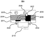
207:リチウムイオンの移動方向
208:電極間に形成された電界
209:着色
210:電源
221:絶縁性基板
222:第1の電極
223:第2の電極
224:電解質層
225:エレクトロクロミック層
226:リチウムイオン
227:リチウムイオンの移動方向
228:電極間に形成された電界
229:着色
230:電源
301:着色パルス
302:消色パルス
303:着色状態
304:消色状態
305:着色パルス
311:ポリカーボネート基板
312:ITO電極
313:ITO電極
314:エレクトロクロミック層
315:電解質層
316:絶縁層
317:ITO電極
318:ITO電極
319:エレクトロクロミック層
320:電解質層
321:基板
322:第1の透明電極
323:第2の透明電極
324:エレクトロクロミック層
325:電解質層
326:エレクトロクロミック層の着色部分
327:電源
328:レーザ光
331:保護層
333:電解質層
334:エレクトロクロミック層
335:電極層
336:紫外線硬化樹脂層
337:貼り合せ保護基板
338:基板
339:グルーブ部
340:ランド部
341:入射レーザ光
351:中心線
352:ディスク中心の穴部分
353:電極
354:絶縁部分
355:電極
356:エレクトロクロミック層
357:電解質層
358:絶縁部分
359:電極を分離するための絶縁部分
360:情報記録部分
361:ディスク下面
371:ダミー基板
372:絶縁部分
373:レジストパターン
374:エッチング工程
375:電極スパッタ工程
376:レジスト除去工程
377:電極形成工程
378:エレクトロクロミック層・電解質層形成工程
379:エレクトロクロミック層
380:電解質層
381:絶縁部分および電極形成工程とダミー基板除去
391:保護層
393:電解質層
394:エレクトロクロミック層
395:電極層
396:紫外線硬化樹脂層
397:貼り合せ保護基板
398:基板
399:グルーブ部
400:ランド部
401:入射レーザ光
411:消色時のスペクトル
412:着色時のスペクトル
421:記録・再生に必要な着色濃度
431:光ディスク
432:8−16変調器
433:記録波形発生回路
434:レーザ駆動回路
435:光ヘッド
436:8−16復調器
437:プリアンプ回路
438:L/Gサーボ回路
439:モータ
440:信号入力
441:信号出力
451:消色時のスペクトル
452:着色時のスペクトル
461:層選択信号
462:可変電源
463:層選択回路
464:電流制御器
465:第1層選択の信号
466:第2層選択の信号
467:第3層選択の信号
468:第4層選択の信号
471:ポリカーボネート基板
472:SiO2層
473:IZO透明電極
474:エレクトロクロミック層
475:電解質層
476:ZnS・SiO2絶縁層
477:ポリカーボネート基板
478:第1層
479:第2層
480:第3層
481:第4層
491:保護層
492:第1の電極層
493:電解質層
494:エレクトロクロミック層
495:第2の電極層
496:紫外線硬化樹脂層
497:貼り合せ保護基板
498:基板
499:グルーブ部
500:ランド部
511:ディスク中心の穴部分
512:記録領域
513:絶縁部分
514:電極
515:絶縁部分
516:電極
517:絶縁部分
518:電極
519:絶縁部分
520:電極
531:ガラス基板
532:第1の電極
533:第1の電極への配線
534:第2の電極
535:第2の電極への配線
536:中心横断線
541:ガラス基板
542:第1の電極
543:第2の電極
544:電解質層
545;エレクトロクロミック層
546:絶縁保護層
551:第1層のガラス基板
552:第1の電極(第1列)への配線
553:第1の電極(第2列)への配線
554:第1の電極
555:第2の電極(第1列)への配線
556:第2の電極(第2列)への配線
557:第2の電極
558:第2層
559:第3層
560:第4層
561:反射層および下部保護層
562:レーザ光の入射方向
563:貫通方向線
571:絶縁層
572:透明電極層
573:電解質層
574:エレクトロクロミック層
575:上部絶縁保護層
576:下部絶縁保護層
577:反射層
581:第1層
582:第2層
583:第3層
584:第4層
585:レーザ光の入射方向
601:基板
602:第1の電極
603:第1の電極への配線
604:第2の電極
605:第3の電極
606:第4の電極
607:第5の電極
608:第2から第5の電極への配線
609:中心横断線
611:基板
612:第1の電極
613:第2の電極
614:第3の電極
615:第4の電極
616:第5の電極
617:電解質層
618:エレクトロクロミック層
619:保護層
621:基板
622:第1の電極
623:第1の電極への配線
624:第2の電極
625:第3の電極
626:第4の電極
627:第5の電極
628:第2から第5の電極への配線
629:中心横断線
631:基板
632:第1の電極
633:第2の電極
634:第3の電極
635:第4の電極
636:第5の電極
637:電解質層
638:エレクトロクロミック層
639:保護層
641:着色部分
642:着色部分
643:着色部分
644:着色部分
661:第1層のガラス基板
662:配線
663:配線
664:第1のエレクトロクロミック単位セル
665:配線
666:配線
667:電極
668:第2層
669:第3層
670:第4層
671:反射層および下部保護層
672:レーザ光の入射方向
673:貫通方向線
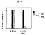
701:規格化された透過率変調度の初期値
702:規格化された1000回後の透過率変調度。
Claims (20)
- 第1の絶縁部材と、
前記第1の絶縁部材の一の平面内に形成された第1および第2の電極と、
前記第1および第2の電極と導通するように設けられたエレクトロクロミック材料を含む第1の導電層を有し、
前記第1、第2の電極間は絶縁されていることを特徴とする情報記録媒体。 - 前記第1の導電層は、
前記第1および第2の電極に接して形成された、前記エレクトロクロミック材料を含むエレクトロクロミック層と、
前記エレクトロクロミック層に接し、前記エレクトロクロミック層へ拡散するイオンを含む電解質層とを有することを特徴とする請求項1記載の情報記録媒体。 - 前記第1の導電層は、
前記第1および第2の電極に接して形成された電解質層と、
前記電解質層に接し、前記エレクトロクロミック材料を含むエレクトロクロミック層とを有することを特徴とする請求項1記載の情報記録媒体。 - 前記第1の導電層は、導電性高分子エレクトロクロミック材料である、ポリチオフェンおよびその誘導体、ポリピロールおよびその誘導体、ポリアニリンおよびその誘導体、ポリ(トリメチルシリルフェニルアセチレン)、ポリ(ジアルコキシフェニレンビニレン)、の中から選ばれた少なくとも1つの化合物を含むことを特徴とする請求項1記載の情報記録媒体。
- 前記第1の導電層は、酸化タングステン、酸化イリジウム、酸化ニッケル、酸化チタン、五酸化バナジウムから選ばれた少なくとも1つの化合物を含むことを特徴とする請求項1に記載の情報記録媒体。
- 前記第1の導電層は、ビオローゲン、炭素数1から20のアルキル基を有するアルキルビオローゲン、金属フタロシアニン錯体、ポルフィリン誘導体、バソフェナントロリン錯体から選ばれた少なくとも1つの化合物を含むことを特徴とする請求項1に記載の情報記録媒体。
- 前記第1および第2の電極は、ITO(indium tin oxide)、IZO(indium zinc oxide)、酸化スズSnO2のいずれかであることを特徴とする請求項1記載の情報記録媒体。
- 前記第1の導電層上に第2の絶縁部材を有し、
前記第2の絶縁部材の一の平面内に形成された第3および第4の電極と、
前記第3および第4の電極と導通するように設けられたエレクトロクロミック材料を含む第2の導電層を有し、
前記第3、第4の電極間は絶縁されていることを特徴とする請求項1記載の情報記録媒体。 - 前記第1の導電層は、
前記第1および第2の電極に接して形成された、前記エレクトロクロミック材料を含む第1のエレクトロクロミック層と、
前記第1のエレクトロクロミック層に接し、前記エレクトロクロミック層へ拡散するイオンを含む第1の電解質層とを有し、
前記第2の導電層は、
前記第3および第4の電極に接して形成された、前記エレクトロクロミック材料を含む第2のエレクトロクロミック層と、
前記第2のエレクトロクロミック層に接し、前記エレクトロクロミック層へ拡散するイオンを含む第2の電解質層とを有することを特徴とする請求項8記載の情報記録媒体。 - 前記第1の導電層は、
前記第1および第2の電極に接して形成された第1の層と、
前記電解質層に接し、前記エレクトロクロミック材料を含む第1のエレクトロクロミック層とを有し、
前記第2の導電層は、
前記第3および第4の電極に接して形成された第2の層と、
前記電解質層に接し、前記エレクトロクロミック材料を含む第2のエレクトロクロミック層とを有することを特徴とする請求項8記載の情報記録媒体。 - 絶縁部材と、
前記絶縁部材の一の平面内に形成された第1および第2および第3の電極と、
前記第1および第2の電極との間および、前記第1および第3の電極との間を導通するように設けられたエレクトロクロミック材料を含む導電層を有し、
前記第1の電極と前記第2の電極と前記第3の電極の間はそれぞれ絶縁されていることを特徴とする情報記録媒体。 - 前記第1の電極に正の電圧がかけられ、前記第2および第3の電極には負の電圧がかけられることを特徴とする請求項11記載の情報記録媒体。
- 前記第1の電極に負の電圧がかけられ、前記第2および第3の電極には正の電圧がかけられることを特徴とする請求項11記載の情報記録媒体。
- 前記第1および第2の電極間、または前記第1および第3の電極間の少なくとも一方に電圧がかけられることを特徴とする請求項11記載の情報記録媒体。
- 前記導電層は、
前記第1および第2および第3の電極に接して形成された、前記エレクトロクロミック材料を含むエレクトロクロミック層と、
前記エレクトロクロミック層に接し、前記エレクトロクロミック層へ拡散するイオンを含む電解質層とを有することを特徴とする請求項11記載の情報記録媒体。 - 前記導電層は、
前記第1および第2および第3の電極に接して形成された電解質層と、
前記電解質層に接し、前記エレクトロクロミック材料を含むエレクトロクロミック層とを有することを特徴とする請求項11記載の情報記録媒体。 - 第1の絶縁部材と、前記絶縁部材の一の平面内に形成された第1および第2の電極と、前記第1および第2の電極と導通するように設けられたエレクトロクロミック材料を含む第1の導電層を有し、前記第1、第2の電極間は絶縁されている情報記録媒体に対して、情報を記録し、または前記情報記録媒体から情報を読み出すための情報記録装置であって、
前記第1および第2の電極間に電圧を印加する電源と、
前記情報記録媒体に光を照射する光源とを有することを特徴とする情報記録装置。 - 前記情報記録媒体は、前記第1の導電層上に第2の絶縁部材を有し、前記第2の絶縁部材の一の平面内に形成された第3および第4の電極と、前記第3および第4の電極と導通するように設けられたエレクトロクロミック材料を含む第2の導電層を有し、前記第3、第4の電極間は絶縁されており、
前記電源は、前記第1および第2の電極間、または前記第3および第4の電極間の少なくとも一方に電圧を印加することを特徴とする請求項17記載の情報記録装置。 - 前記光源から照射され、前記情報記録媒体で反射された光を検出する検出器を有することを特徴とする請求項17記載の情報記録装置。
- 絶縁部材と、絶縁部材の一の平面内に形成された第1および第2の電極と、前記第1および第2の電極と導通するように設けられたエレクトロクロミック材料を含む導電層を有し、前記第1、第2の電極間は絶縁されている情報記録媒体に対して、前記第1および第2の電極間に電圧を印加し、前記導電層を着色するステップと、
着色された前記導電層に対して光を照射し情報を記録するステップとを有することを特徴とする情報記録方法。
Priority Applications (2)
| Application Number | Priority Date | Filing Date | Title |
|---|---|---|---|
| JP2004212461A JP2006031889A (ja) | 2004-07-21 | 2004-07-21 | 情報記録媒体、情報記録装置および情報記録方法 |
| US10/928,284 US7351460B2 (en) | 2004-07-21 | 2004-08-30 | Information recording medium, information recording device, and information recording method |
Applications Claiming Priority (1)
| Application Number | Priority Date | Filing Date | Title |
|---|---|---|---|
| JP2004212461A JP2006031889A (ja) | 2004-07-21 | 2004-07-21 | 情報記録媒体、情報記録装置および情報記録方法 |
Publications (2)
| Publication Number | Publication Date |
|---|---|
| JP2006031889A true JP2006031889A (ja) | 2006-02-02 |
| JP2006031889A5 JP2006031889A5 (ja) | 2007-05-24 |
Family
ID=35656992
Family Applications (1)
| Application Number | Title | Priority Date | Filing Date |
|---|---|---|---|
| JP2004212461A Pending JP2006031889A (ja) | 2004-07-21 | 2004-07-21 | 情報記録媒体、情報記録装置および情報記録方法 |
Country Status (2)
| Country | Link |
|---|---|
| US (1) | US7351460B2 (ja) |
| JP (1) | JP2006031889A (ja) |
Families Citing this family (12)
| Publication number | Priority date | Publication date | Assignee | Title |
|---|---|---|---|---|
| CN100353434C (zh) * | 2004-03-16 | 2007-12-05 | 松下电器产业株式会社 | 光学元件、光头、光信息装置以及光头的控制方法 |
| US7935404B2 (en) * | 2005-01-31 | 2011-05-03 | Hewlett-Packard Development Company, L.P. | System and method for marking an optical disk |
| JP2007102989A (ja) * | 2005-09-12 | 2007-04-19 | Hitachi Ltd | 情報記録媒体及びその製造方法 |
| US8202598B2 (en) * | 2005-11-21 | 2012-06-19 | Nbcuniversal Media, Llc | Optical article having an electrically responsive layer as an anti-theft feature and a system and method for inhibiting theft |
| US20070122735A1 (en) * | 2005-11-30 | 2007-05-31 | Wisnudel Marc B | Optical storage device having limited-use content and method for making same |
| TWI273131B (en) * | 2005-12-29 | 2007-02-11 | Ind Tech Res Inst | Electrochromic film |
| KR101536101B1 (ko) * | 2007-08-02 | 2015-07-13 | 어플라이드 머티어리얼스, 인코포레이티드 | 박막 반도체 물질들을 이용하는 박막 트랜지스터들 |
| US20110037575A1 (en) * | 2008-01-31 | 2011-02-17 | Dieter Horst | Method and Apparatus for Providing Energy to Passive Tags in a Radio-frequency Identification System |
| US8488428B2 (en) * | 2008-05-14 | 2013-07-16 | Nbcuniversal Media, Llc | Enhanced security of optical article |
| US9195883B2 (en) | 2012-04-09 | 2015-11-24 | Avigilon Fortress Corporation | Object tracking and best shot detection system |
| KR20140001502A (ko) * | 2012-06-27 | 2014-01-07 | 엘지이노텍 주식회사 | 전기변색소자 및 그 제조 방법 |
| KR102319360B1 (ko) * | 2017-09-28 | 2021-10-29 | 주식회사 엘지화학 | 전기 변색 복합체, 이를 포함하는 전기 변색 소자 및 전기 변색 소자의 제조방법 |
Family Cites Families (21)
| Publication number | Priority date | Publication date | Assignee | Title |
|---|---|---|---|---|
| JPS60224136A (ja) * | 1984-04-23 | 1985-11-08 | Matsushita Electric Ind Co Ltd | 光学記録材料および記録方法 |
| JPS61133065A (ja) * | 1984-12-03 | 1986-06-20 | Hitachi Ltd | 光情報記録装置 |
| GB8606651D0 (en) * | 1986-03-18 | 1986-04-23 | Green M | Electrochromic data recording systems |
| JPS63122032A (ja) | 1986-11-12 | 1988-05-26 | Hitachi Ltd | 電界効果型光デイスク |
| US6559903B2 (en) * | 1991-11-27 | 2003-05-06 | Reveo, Inc. | Non-absorptive electro-optical glazing structure employing composite infrared reflective polarizing filter |
| JPH11185288A (ja) | 1997-12-17 | 1999-07-09 | Takeshi Aoki | 光ディスクおよび光ディスク装置 |
| JP2000292818A (ja) * | 1999-04-07 | 2000-10-20 | Fuji Photo Film Co Ltd | 光書込み表示素子及びそれを用いた光書込み表示装置 |
| US6597489B1 (en) * | 1999-06-30 | 2003-07-22 | Gentex Corporation | Electrode design for electrochromic devices |
| JP2002082360A (ja) | 2000-09-11 | 2002-03-22 | Fuji Photo Film Co Ltd | 光書き込み型記録材料 |
| JP2002192833A (ja) * | 2000-12-27 | 2002-07-10 | Fuji Photo Film Co Ltd | 画像記録方法及び画像記録装置並びにこれに用いる記録シート |
| US6556470B1 (en) * | 2001-07-31 | 2003-04-29 | Hewlett-Packard Company | Field addressable rewritable media |
| DE60302378T2 (de) * | 2002-03-22 | 2006-08-03 | Ricoh Co. | Optisches Aufzeichnungsmedium und zugehöriges Aufzeichnungsverfahren |
| JP4120268B2 (ja) * | 2002-05-27 | 2008-07-16 | 株式会社日立製作所 | 情報記録媒体および情報記録方法 |
| JP3849606B2 (ja) * | 2002-08-06 | 2006-11-22 | 株式会社日立製作所 | 情報記録媒体、情報記録方法、情報再生方法 |
| DE602004002575T2 (de) * | 2003-02-27 | 2007-05-31 | Koninklijke Philips Electronics N.V. | Mehrstapel-informationsträger mit elektrochromischen materialien |
| JP2004310912A (ja) * | 2003-04-08 | 2004-11-04 | Hitachi Ltd | 情報記録方法および情報記録装置 |
| EP1649457A2 (en) * | 2003-07-18 | 2006-04-26 | Koninklijke Philips Electronics N.V. | Multi-layer information carrier with switching circuit |
| JP2005078722A (ja) * | 2003-09-01 | 2005-03-24 | Hitachi Ltd | 情報記録装置、情報記録媒体及び情報記録方法 |
| US20050052983A1 (en) * | 2003-09-09 | 2005-03-10 | Vincent Kent D. | Method and apparatus for electro-optical disk memory |
| US20050276211A1 (en) * | 2004-06-09 | 2005-12-15 | Akemi Hirotsune | Information recording medium and manufacturing process |
| JP2007149225A (ja) * | 2005-11-28 | 2007-06-14 | Hitachi Ltd | 情報記録装置 |
-
2004
- 2004-07-21 JP JP2004212461A patent/JP2006031889A/ja active Pending
- 2004-08-30 US US10/928,284 patent/US7351460B2/en not_active Expired - Fee Related
Also Published As
| Publication number | Publication date |
|---|---|
| US7351460B2 (en) | 2008-04-01 |
| US20060018231A1 (en) | 2006-01-26 |
Similar Documents
| Publication | Publication Date | Title |
|---|---|---|
| JP4685507B2 (ja) | エレクトロクロミックデバイス | |
| JP4120268B2 (ja) | 情報記録媒体および情報記録方法 | |
| JP4079068B2 (ja) | 情報記録媒体および情報記録方法 | |
| JP3969377B2 (ja) | 情報記録媒体および情報記録方法 | |
| US20050276211A1 (en) | Information recording medium and manufacturing process | |
| JP2006031889A (ja) | 情報記録媒体、情報記録装置および情報記録方法 | |
| US7349319B2 (en) | Information recording apparatus, recording media and recording method | |
| US7263053B2 (en) | Information recording method and information recording apparatus | |
| JP2006228358A (ja) | 情報記録媒体およびその製造方法 | |
| KR20050115247A (ko) | 전자착색 재료를 사용한 다중 적층체 정보매체 | |
| JP4165511B2 (ja) | 情報記録装置 | |
| JP2004273055A (ja) | 情報保持媒体、情報記録方法および装置 | |
| JP4676372B2 (ja) | 多層光記録媒体、情報記録方法及び情報再生方法 | |
| JP4100398B2 (ja) | 情報記録媒体 | |
| US7203152B2 (en) | Multi-stack rolled-up information carrier | |
| JP2006012224A (ja) | 情報記録媒体およびその製造方法 | |
| JP2005203046A (ja) | 情報記録媒体、情報記録方法及び記録装置 | |
| JP2007102989A (ja) | 情報記録媒体及びその製造方法 | |
| JP2006066019A (ja) | 記録媒体 | |
| JP2006519451A (ja) | エレクトロクロミック材料を伴うマルチスタック型蛍光性情報担体 | |
| JP2008165898A (ja) | 多層光記録媒体、情報記録方法及び情報再生方法 |
Legal Events
| Date | Code | Title | Description |
|---|---|---|---|
| RD04 | Notification of resignation of power of attorney |
Free format text: JAPANESE INTERMEDIATE CODE: A7424 Effective date: 20060424 |
|
| A521 | Request for written amendment filed |
Free format text: JAPANESE INTERMEDIATE CODE: A523 Effective date: 20070329 |
|
| A621 | Written request for application examination |
Free format text: JAPANESE INTERMEDIATE CODE: A621 Effective date: 20070329 |
|
| A977 | Report on retrieval |
Free format text: JAPANESE INTERMEDIATE CODE: A971007 Effective date: 20081010 |
|
| A131 | Notification of reasons for refusal |
Free format text: JAPANESE INTERMEDIATE CODE: A131 Effective date: 20081125 |
|
| A02 | Decision of refusal |
Free format text: JAPANESE INTERMEDIATE CODE: A02 Effective date: 20090324 |