JP2005524239A - Direct connect signal system - Google Patents
Direct connect signal system Download PDFInfo
- Publication number
- JP2005524239A JP2005524239A JP2004502330A JP2004502330A JP2005524239A JP 2005524239 A JP2005524239 A JP 2005524239A JP 2004502330 A JP2004502330 A JP 2004502330A JP 2004502330 A JP2004502330 A JP 2004502330A JP 2005524239 A JP2005524239 A JP 2005524239A
- Authority
- JP
- Japan
- Prior art keywords
- integrated circuit
- substrate
- circuit package
- die
- cable
- Prior art date
- Legal status (The legal status is an assumption and is not a legal conclusion. Google has not performed a legal analysis and makes no representation as to the accuracy of the status listed.)
- Withdrawn
Links
Images


Classifications
-
- H—ELECTRICITY
- H05—ELECTRIC TECHNIQUES NOT OTHERWISE PROVIDED FOR
- H05K—PRINTED CIRCUITS; CASINGS OR CONSTRUCTIONAL DETAILS OF ELECTRIC APPARATUS; MANUFACTURE OF ASSEMBLAGES OF ELECTRICAL COMPONENTS
- H05K1/00—Printed circuits
- H05K1/02—Details
- H05K1/14—Structural association of two or more printed circuits
- H05K1/147—Structural association of two or more printed circuits at least one of the printed circuits being bent or folded, e.g. by using a flexible printed circuit
-
- H—ELECTRICITY
- H01—ELECTRIC ELEMENTS
- H01L—SEMICONDUCTOR DEVICES NOT COVERED BY CLASS H10
- H01L23/00—Details of semiconductor or other solid state devices
- H01L23/48—Arrangements for conducting electric current to or from the solid state body in operation, e.g. leads, terminal arrangements ; Selection of materials therefor
- H01L23/488—Arrangements for conducting electric current to or from the solid state body in operation, e.g. leads, terminal arrangements ; Selection of materials therefor consisting of soldered or bonded constructions
- H01L23/498—Leads, i.e. metallisations or lead-frames on insulating substrates, e.g. chip carriers
- H01L23/49805—Leads, i.e. metallisations or lead-frames on insulating substrates, e.g. chip carriers the leads being also applied on the sidewalls or the bottom of the substrate, e.g. leadless packages for surface mounting
-
- H—ELECTRICITY
- H05—ELECTRIC TECHNIQUES NOT OTHERWISE PROVIDED FOR
- H05K—PRINTED CIRCUITS; CASINGS OR CONSTRUCTIONAL DETAILS OF ELECTRIC APPARATUS; MANUFACTURE OF ASSEMBLAGES OF ELECTRICAL COMPONENTS
- H05K3/00—Apparatus or processes for manufacturing printed circuits
- H05K3/22—Secondary treatment of printed circuits
- H05K3/222—Completing of printed circuits by adding non-printed jumper connections
-
- H—ELECTRICITY
- H01—ELECTRIC ELEMENTS
- H01L—SEMICONDUCTOR DEVICES NOT COVERED BY CLASS H10
- H01L2224/00—Indexing scheme for arrangements for connecting or disconnecting semiconductor or solid-state bodies and methods related thereto as covered by H01L24/00
- H01L2224/01—Means for bonding being attached to, or being formed on, the surface to be connected, e.g. chip-to-package, die-attach, "first-level" interconnects; Manufacturing methods related thereto
- H01L2224/02—Bonding areas; Manufacturing methods related thereto
- H01L2224/04—Structure, shape, material or disposition of the bonding areas prior to the connecting process
- H01L2224/05—Structure, shape, material or disposition of the bonding areas prior to the connecting process of an individual bonding area
- H01L2224/0554—External layer
- H01L2224/05599—Material
-
- H—ELECTRICITY
- H01—ELECTRIC ELEMENTS
- H01L—SEMICONDUCTOR DEVICES NOT COVERED BY CLASS H10
- H01L2224/00—Indexing scheme for arrangements for connecting or disconnecting semiconductor or solid-state bodies and methods related thereto as covered by H01L24/00
- H01L2224/01—Means for bonding being attached to, or being formed on, the surface to be connected, e.g. chip-to-package, die-attach, "first-level" interconnects; Manufacturing methods related thereto
- H01L2224/10—Bump connectors; Manufacturing methods related thereto
- H01L2224/15—Structure, shape, material or disposition of the bump connectors after the connecting process
- H01L2224/16—Structure, shape, material or disposition of the bump connectors after the connecting process of an individual bump connector
- H01L2224/161—Disposition
- H01L2224/16151—Disposition the bump connector connecting between a semiconductor or solid-state body and an item not being a semiconductor or solid-state body, e.g. chip-to-substrate, chip-to-passive
- H01L2224/16221—Disposition the bump connector connecting between a semiconductor or solid-state body and an item not being a semiconductor or solid-state body, e.g. chip-to-substrate, chip-to-passive the body and the item being stacked
- H01L2224/16225—Disposition the bump connector connecting between a semiconductor or solid-state body and an item not being a semiconductor or solid-state body, e.g. chip-to-substrate, chip-to-passive the body and the item being stacked the item being non-metallic, e.g. insulating substrate with or without metallisation
-
- H—ELECTRICITY
- H01—ELECTRIC ELEMENTS
- H01L—SEMICONDUCTOR DEVICES NOT COVERED BY CLASS H10
- H01L2224/00—Indexing scheme for arrangements for connecting or disconnecting semiconductor or solid-state bodies and methods related thereto as covered by H01L24/00
- H01L2224/01—Means for bonding being attached to, or being formed on, the surface to be connected, e.g. chip-to-package, die-attach, "first-level" interconnects; Manufacturing methods related thereto
- H01L2224/26—Layer connectors, e.g. plate connectors, solder or adhesive layers; Manufacturing methods related thereto
- H01L2224/31—Structure, shape, material or disposition of the layer connectors after the connecting process
- H01L2224/32—Structure, shape, material or disposition of the layer connectors after the connecting process of an individual layer connector
- H01L2224/321—Disposition
- H01L2224/32151—Disposition the layer connector connecting between a semiconductor or solid-state body and an item not being a semiconductor or solid-state body, e.g. chip-to-substrate, chip-to-passive
- H01L2224/32221—Disposition the layer connector connecting between a semiconductor or solid-state body and an item not being a semiconductor or solid-state body, e.g. chip-to-substrate, chip-to-passive the body and the item being stacked
- H01L2224/32225—Disposition the layer connector connecting between a semiconductor or solid-state body and an item not being a semiconductor or solid-state body, e.g. chip-to-substrate, chip-to-passive the body and the item being stacked the item being non-metallic, e.g. insulating substrate with or without metallisation
-
- H—ELECTRICITY
- H01—ELECTRIC ELEMENTS
- H01L—SEMICONDUCTOR DEVICES NOT COVERED BY CLASS H10
- H01L2224/00—Indexing scheme for arrangements for connecting or disconnecting semiconductor or solid-state bodies and methods related thereto as covered by H01L24/00
- H01L2224/01—Means for bonding being attached to, or being formed on, the surface to be connected, e.g. chip-to-package, die-attach, "first-level" interconnects; Manufacturing methods related thereto
- H01L2224/26—Layer connectors, e.g. plate connectors, solder or adhesive layers; Manufacturing methods related thereto
- H01L2224/31—Structure, shape, material or disposition of the layer connectors after the connecting process
- H01L2224/32—Structure, shape, material or disposition of the layer connectors after the connecting process of an individual layer connector
- H01L2224/321—Disposition
- H01L2224/32151—Disposition the layer connector connecting between a semiconductor or solid-state body and an item not being a semiconductor or solid-state body, e.g. chip-to-substrate, chip-to-passive
- H01L2224/32221—Disposition the layer connector connecting between a semiconductor or solid-state body and an item not being a semiconductor or solid-state body, e.g. chip-to-substrate, chip-to-passive the body and the item being stacked
- H01L2224/32245—Disposition the layer connector connecting between a semiconductor or solid-state body and an item not being a semiconductor or solid-state body, e.g. chip-to-substrate, chip-to-passive the body and the item being stacked the item being metallic
-
- H—ELECTRICITY
- H01—ELECTRIC ELEMENTS
- H01L—SEMICONDUCTOR DEVICES NOT COVERED BY CLASS H10
- H01L2224/00—Indexing scheme for arrangements for connecting or disconnecting semiconductor or solid-state bodies and methods related thereto as covered by H01L24/00
- H01L2224/01—Means for bonding being attached to, or being formed on, the surface to be connected, e.g. chip-to-package, die-attach, "first-level" interconnects; Manufacturing methods related thereto
- H01L2224/42—Wire connectors; Manufacturing methods related thereto
- H01L2224/44—Structure, shape, material or disposition of the wire connectors prior to the connecting process
- H01L2224/45—Structure, shape, material or disposition of the wire connectors prior to the connecting process of an individual wire connector
- H01L2224/45001—Core members of the connector
- H01L2224/45099—Material
-
- H—ELECTRICITY
- H01—ELECTRIC ELEMENTS
- H01L—SEMICONDUCTOR DEVICES NOT COVERED BY CLASS H10
- H01L2224/00—Indexing scheme for arrangements for connecting or disconnecting semiconductor or solid-state bodies and methods related thereto as covered by H01L24/00
- H01L2224/01—Means for bonding being attached to, or being formed on, the surface to be connected, e.g. chip-to-package, die-attach, "first-level" interconnects; Manufacturing methods related thereto
- H01L2224/42—Wire connectors; Manufacturing methods related thereto
- H01L2224/47—Structure, shape, material or disposition of the wire connectors after the connecting process
- H01L2224/48—Structure, shape, material or disposition of the wire connectors after the connecting process of an individual wire connector
- H01L2224/4805—Shape
- H01L2224/4809—Loop shape
- H01L2224/48091—Arched
-
- H—ELECTRICITY
- H01—ELECTRIC ELEMENTS
- H01L—SEMICONDUCTOR DEVICES NOT COVERED BY CLASS H10
- H01L2224/00—Indexing scheme for arrangements for connecting or disconnecting semiconductor or solid-state bodies and methods related thereto as covered by H01L24/00
- H01L2224/01—Means for bonding being attached to, or being formed on, the surface to be connected, e.g. chip-to-package, die-attach, "first-level" interconnects; Manufacturing methods related thereto
- H01L2224/42—Wire connectors; Manufacturing methods related thereto
- H01L2224/47—Structure, shape, material or disposition of the wire connectors after the connecting process
- H01L2224/48—Structure, shape, material or disposition of the wire connectors after the connecting process of an individual wire connector
- H01L2224/481—Disposition
- H01L2224/48151—Connecting between a semiconductor or solid-state body and an item not being a semiconductor or solid-state body, e.g. chip-to-substrate, chip-to-passive
- H01L2224/48221—Connecting between a semiconductor or solid-state body and an item not being a semiconductor or solid-state body, e.g. chip-to-substrate, chip-to-passive the body and the item being stacked
- H01L2224/48245—Connecting between a semiconductor or solid-state body and an item not being a semiconductor or solid-state body, e.g. chip-to-substrate, chip-to-passive the body and the item being stacked the item being metallic
- H01L2224/48247—Connecting between a semiconductor or solid-state body and an item not being a semiconductor or solid-state body, e.g. chip-to-substrate, chip-to-passive the body and the item being stacked the item being metallic connecting the wire to a bond pad of the item
-
- H—ELECTRICITY
- H01—ELECTRIC ELEMENTS
- H01L—SEMICONDUCTOR DEVICES NOT COVERED BY CLASS H10
- H01L2224/00—Indexing scheme for arrangements for connecting or disconnecting semiconductor or solid-state bodies and methods related thereto as covered by H01L24/00
- H01L2224/01—Means for bonding being attached to, or being formed on, the surface to be connected, e.g. chip-to-package, die-attach, "first-level" interconnects; Manufacturing methods related thereto
- H01L2224/42—Wire connectors; Manufacturing methods related thereto
- H01L2224/47—Structure, shape, material or disposition of the wire connectors after the connecting process
- H01L2224/48—Structure, shape, material or disposition of the wire connectors after the connecting process of an individual wire connector
- H01L2224/484—Connecting portions
- H01L2224/48463—Connecting portions the connecting portion on the bonding area of the semiconductor or solid-state body being a ball bond
-
- H—ELECTRICITY
- H01—ELECTRIC ELEMENTS
- H01L—SEMICONDUCTOR DEVICES NOT COVERED BY CLASS H10
- H01L2224/00—Indexing scheme for arrangements for connecting or disconnecting semiconductor or solid-state bodies and methods related thereto as covered by H01L24/00
- H01L2224/73—Means for bonding being of different types provided for in two or more of groups H01L2224/10, H01L2224/18, H01L2224/26, H01L2224/34, H01L2224/42, H01L2224/50, H01L2224/63, H01L2224/71
- H01L2224/732—Location after the connecting process
- H01L2224/73201—Location after the connecting process on the same surface
- H01L2224/73203—Bump and layer connectors
- H01L2224/73204—Bump and layer connectors the bump connector being embedded into the layer connector
-
- H—ELECTRICITY
- H01—ELECTRIC ELEMENTS
- H01L—SEMICONDUCTOR DEVICES NOT COVERED BY CLASS H10
- H01L2224/00—Indexing scheme for arrangements for connecting or disconnecting semiconductor or solid-state bodies and methods related thereto as covered by H01L24/00
- H01L2224/73—Means for bonding being of different types provided for in two or more of groups H01L2224/10, H01L2224/18, H01L2224/26, H01L2224/34, H01L2224/42, H01L2224/50, H01L2224/63, H01L2224/71
- H01L2224/732—Location after the connecting process
- H01L2224/73251—Location after the connecting process on different surfaces
- H01L2224/73253—Bump and layer connectors
-
- H—ELECTRICITY
- H01—ELECTRIC ELEMENTS
- H01L—SEMICONDUCTOR DEVICES NOT COVERED BY CLASS H10
- H01L2224/00—Indexing scheme for arrangements for connecting or disconnecting semiconductor or solid-state bodies and methods related thereto as covered by H01L24/00
- H01L2224/73—Means for bonding being of different types provided for in two or more of groups H01L2224/10, H01L2224/18, H01L2224/26, H01L2224/34, H01L2224/42, H01L2224/50, H01L2224/63, H01L2224/71
- H01L2224/732—Location after the connecting process
- H01L2224/73251—Location after the connecting process on different surfaces
- H01L2224/73265—Layer and wire connectors
-
- H—ELECTRICITY
- H01—ELECTRIC ELEMENTS
- H01L—SEMICONDUCTOR DEVICES NOT COVERED BY CLASS H10
- H01L2224/00—Indexing scheme for arrangements for connecting or disconnecting semiconductor or solid-state bodies and methods related thereto as covered by H01L24/00
- H01L2224/80—Methods for connecting semiconductor or other solid state bodies using means for bonding being attached to, or being formed on, the surface to be connected
- H01L2224/85—Methods for connecting semiconductor or other solid state bodies using means for bonding being attached to, or being formed on, the surface to be connected using a wire connector
- H01L2224/8538—Bonding interfaces outside the semiconductor or solid-state body
- H01L2224/85399—Material
-
- H—ELECTRICITY
- H01—ELECTRIC ELEMENTS
- H01L—SEMICONDUCTOR DEVICES NOT COVERED BY CLASS H10
- H01L24/00—Arrangements for connecting or disconnecting semiconductor or solid-state bodies; Methods or apparatus related thereto
- H01L24/01—Means for bonding being attached to, or being formed on, the surface to be connected, e.g. chip-to-package, die-attach, "first-level" interconnects; Manufacturing methods related thereto
- H01L24/10—Bump connectors ; Manufacturing methods related thereto
- H01L24/15—Structure, shape, material or disposition of the bump connectors after the connecting process
- H01L24/16—Structure, shape, material or disposition of the bump connectors after the connecting process of an individual bump connector
-
- H—ELECTRICITY
- H01—ELECTRIC ELEMENTS
- H01L—SEMICONDUCTOR DEVICES NOT COVERED BY CLASS H10
- H01L24/00—Arrangements for connecting or disconnecting semiconductor or solid-state bodies; Methods or apparatus related thereto
- H01L24/01—Means for bonding being attached to, or being formed on, the surface to be connected, e.g. chip-to-package, die-attach, "first-level" interconnects; Manufacturing methods related thereto
- H01L24/42—Wire connectors; Manufacturing methods related thereto
- H01L24/47—Structure, shape, material or disposition of the wire connectors after the connecting process
- H01L24/48—Structure, shape, material or disposition of the wire connectors after the connecting process of an individual wire connector
-
- H—ELECTRICITY
- H01—ELECTRIC ELEMENTS
- H01L—SEMICONDUCTOR DEVICES NOT COVERED BY CLASS H10
- H01L2924/00—Indexing scheme for arrangements or methods for connecting or disconnecting semiconductor or solid-state bodies as covered by H01L24/00
- H01L2924/0001—Technical content checked by a classifier
- H01L2924/00014—Technical content checked by a classifier the subject-matter covered by the group, the symbol of which is combined with the symbol of this group, being disclosed without further technical details
-
- H—ELECTRICITY
- H01—ELECTRIC ELEMENTS
- H01L—SEMICONDUCTOR DEVICES NOT COVERED BY CLASS H10
- H01L2924/00—Indexing scheme for arrangements or methods for connecting or disconnecting semiconductor or solid-state bodies as covered by H01L24/00
- H01L2924/01—Chemical elements
- H01L2924/01079—Gold [Au]
-
- H—ELECTRICITY
- H01—ELECTRIC ELEMENTS
- H01L—SEMICONDUCTOR DEVICES NOT COVERED BY CLASS H10
- H01L2924/00—Indexing scheme for arrangements or methods for connecting or disconnecting semiconductor or solid-state bodies as covered by H01L24/00
- H01L2924/10—Details of semiconductor or other solid state devices to be connected
- H01L2924/11—Device type
- H01L2924/14—Integrated circuits
-
- H—ELECTRICITY
- H01—ELECTRIC ELEMENTS
- H01L—SEMICONDUCTOR DEVICES NOT COVERED BY CLASS H10
- H01L2924/00—Indexing scheme for arrangements or methods for connecting or disconnecting semiconductor or solid-state bodies as covered by H01L24/00
- H01L2924/15—Details of package parts other than the semiconductor or other solid state devices to be connected
- H01L2924/151—Die mounting substrate
- H01L2924/153—Connection portion
- H01L2924/1531—Connection portion the connection portion being formed only on the surface of the substrate opposite to the die mounting surface
- H01L2924/15311—Connection portion the connection portion being formed only on the surface of the substrate opposite to the die mounting surface being a ball array, e.g. BGA
-
- H—ELECTRICITY
- H01—ELECTRIC ELEMENTS
- H01L—SEMICONDUCTOR DEVICES NOT COVERED BY CLASS H10
- H01L2924/00—Indexing scheme for arrangements or methods for connecting or disconnecting semiconductor or solid-state bodies as covered by H01L24/00
- H01L2924/15—Details of package parts other than the semiconductor or other solid state devices to be connected
- H01L2924/181—Encapsulation
-
- H—ELECTRICITY
- H01—ELECTRIC ELEMENTS
- H01L—SEMICONDUCTOR DEVICES NOT COVERED BY CLASS H10
- H01L2924/00—Indexing scheme for arrangements or methods for connecting or disconnecting semiconductor or solid-state bodies as covered by H01L24/00
- H01L2924/30—Technical effects
- H01L2924/301—Electrical effects
- H01L2924/30105—Capacitance
-
- H—ELECTRICITY
- H01—ELECTRIC ELEMENTS
- H01L—SEMICONDUCTOR DEVICES NOT COVERED BY CLASS H10
- H01L2924/00—Indexing scheme for arrangements or methods for connecting or disconnecting semiconductor or solid-state bodies as covered by H01L24/00
- H01L2924/30—Technical effects
- H01L2924/301—Electrical effects
- H01L2924/30107—Inductance
-
- H—ELECTRICITY
- H01—ELECTRIC ELEMENTS
- H01L—SEMICONDUCTOR DEVICES NOT COVERED BY CLASS H10
- H01L2924/00—Indexing scheme for arrangements or methods for connecting or disconnecting semiconductor or solid-state bodies as covered by H01L24/00
- H01L2924/30—Technical effects
- H01L2924/301—Electrical effects
- H01L2924/3011—Impedance
-
- H—ELECTRICITY
- H01—ELECTRIC ELEMENTS
- H01L—SEMICONDUCTOR DEVICES NOT COVERED BY CLASS H10
- H01L2924/00—Indexing scheme for arrangements or methods for connecting or disconnecting semiconductor or solid-state bodies as covered by H01L24/00
- H01L2924/30—Technical effects
- H01L2924/301—Electrical effects
- H01L2924/3025—Electromagnetic shielding
-
- H—ELECTRICITY
- H05—ELECTRIC TECHNIQUES NOT OTHERWISE PROVIDED FOR
- H05K—PRINTED CIRCUITS; CASINGS OR CONSTRUCTIONAL DETAILS OF ELECTRIC APPARATUS; MANUFACTURE OF ASSEMBLAGES OF ELECTRICAL COMPONENTS
- H05K1/00—Printed circuits
- H05K1/02—Details
- H05K1/0213—Electrical arrangements not otherwise provided for
- H05K1/0216—Reduction of cross-talk, noise or electromagnetic interference
- H05K1/0228—Compensation of cross-talk by a mutually correlated lay-out of printed circuit traces, e.g. for compensation of cross-talk in mounted connectors
-
- H—ELECTRICITY
- H05—ELECTRIC TECHNIQUES NOT OTHERWISE PROVIDED FOR
- H05K—PRINTED CIRCUITS; CASINGS OR CONSTRUCTIONAL DETAILS OF ELECTRIC APPARATUS; MANUFACTURE OF ASSEMBLAGES OF ELECTRICAL COMPONENTS
- H05K1/00—Printed circuits
- H05K1/02—Details
- H05K1/0213—Electrical arrangements not otherwise provided for
- H05K1/0237—High frequency adaptations
-
- H—ELECTRICITY
- H05—ELECTRIC TECHNIQUES NOT OTHERWISE PROVIDED FOR
- H05K—PRINTED CIRCUITS; CASINGS OR CONSTRUCTIONAL DETAILS OF ELECTRIC APPARATUS; MANUFACTURE OF ASSEMBLAGES OF ELECTRICAL COMPONENTS
- H05K2201/00—Indexing scheme relating to printed circuits covered by H05K1/00
- H05K2201/10—Details of components or other objects attached to or integrated in a printed circuit board
- H05K2201/10227—Other objects, e.g. metallic pieces
- H05K2201/10356—Cables
-
- H—ELECTRICITY
- H05—ELECTRIC TECHNIQUES NOT OTHERWISE PROVIDED FOR
- H05K—PRINTED CIRCUITS; CASINGS OR CONSTRUCTIONAL DETAILS OF ELECTRIC APPARATUS; MANUFACTURE OF ASSEMBLAGES OF ELECTRICAL COMPONENTS
- H05K2201/00—Indexing scheme relating to printed circuits covered by H05K1/00
- H05K2201/10—Details of components or other objects attached to or integrated in a printed circuit board
- H05K2201/10227—Other objects, e.g. metallic pieces
- H05K2201/10378—Interposers
-
- H—ELECTRICITY
- H05—ELECTRIC TECHNIQUES NOT OTHERWISE PROVIDED FOR
- H05K—PRINTED CIRCUITS; CASINGS OR CONSTRUCTIONAL DETAILS OF ELECTRIC APPARATUS; MANUFACTURE OF ASSEMBLAGES OF ELECTRICAL COMPONENTS
- H05K2201/00—Indexing scheme relating to printed circuits covered by H05K1/00
- H05K2201/10—Details of components or other objects attached to or integrated in a printed circuit board
- H05K2201/10431—Details of mounted components
- H05K2201/10507—Involving several components
- H05K2201/1053—Mounted components directly electrically connected to each other, i.e. not via the PCB
-
- H—ELECTRICITY
- H05—ELECTRIC TECHNIQUES NOT OTHERWISE PROVIDED FOR
- H05K—PRINTED CIRCUITS; CASINGS OR CONSTRUCTIONAL DETAILS OF ELECTRIC APPARATUS; MANUFACTURE OF ASSEMBLAGES OF ELECTRICAL COMPONENTS
- H05K2201/00—Indexing scheme relating to printed circuits covered by H05K1/00
- H05K2201/10—Details of components or other objects attached to or integrated in a printed circuit board
- H05K2201/10613—Details of electrical connections of non-printed components, e.g. special leads
- H05K2201/10621—Components characterised by their electrical contacts
- H05K2201/10734—Ball grid array [BGA]; Bump grid array
Abstract
ダイレクトコネクト信号システム(200)は、プリント回路ボード(205)と、このプリント回路ボード上に配置された第1(201A)と第2(201B)の集積回路パッケージとを備える。複数の電気信号導体(203)は、第1と第2の集積回路パッケージの間において、プリント回路ボード上に浮遊させて延在させる。The direct connect signal system (200) includes a printed circuit board (205), and first (201A) and second (201B) integrated circuit packages arranged on the printed circuit board. The plurality of electrical signal conductors (203) are suspended and extended on the printed circuit board between the first and second integrated circuit packages.
Description
本願は、2002年4月29日出願の米国仮特許出願第60/376,482号および2002年7月31日出願の米国仮特許出願第60/400,180号に基づく優先権を主張するものである。尚、米国仮特許出願第60/376,482号および米国仮特許出願第60/400,180号の内容は、本文に援用する。 This application claims priority from US Provisional Patent Application No. 60 / 376,482, filed Apr. 29, 2002, and US Provisional Patent Application No. 60 / 400,180, filed July 31, 2002. It is. The contents of US Provisional Patent Application No. 60 / 376,482 and US Provisional Patent Application No. 60 / 400,180 are incorporated herein by reference.
本発明は、一般的には、電子通信の分野に関し、そして詳細には、集積回路デバイス間における高速シグナリングのための相互接続構造に関するものである。
より速い信号レートに対する絶え間のない要求と歩調を合わせるため、集積回路(IC)パッケージは、ワイヤ・ボンディング形パッケージのような比較的に帯域制限される技術から、図1に示す従来技術のフリップチップ・パッケージ100へと発展してきている。このフリップチップ・パッケージ100は、集積回路ダイ103を含み、これは、多層基板105上にパッド側を下にして装着され、そして非導電性ハウジング101内に封入されている。信号ルーティング構造110は、多層基板105内に配置され、これにより比較的密な配置のダイ・パッド107からの信号を、このパッケージの下面のより散らばったボールグリッドアレイ(BGA)109に再分配している。BGA109の個々のコンタクト・ボールは、次に、プリント回路ボード上の対応するランドに対しハンダ付けすることができる。
The present invention relates generally to the field of electronic communications, and in particular to an interconnect structure for high-speed signaling between integrated circuit devices.
In order to keep pace with the constant demand for faster signal rates, integrated circuit (IC) packages have been developed from relatively band-limited technologies such as wire bonded packages, from the prior art flip chip shown in FIG. -It has evolved into a
フリップチップ・パッケージ100は、一般にワイヤ・ボンディング形パッケージよりも良好な性能を提供するが、信号レートがギガヘルツ・レンジへと深く進行するにつれ、システム設計者に多くの難題を提示する。例えば、信号再分配のため基板105に必要とされる層の数が、ダイ・パッド107の数の増大に応じて常に増してきており、これは、フリップチップ・パッケージ100をより複雑でコスト高のものとする。また、スルーホール・ビア110(すなわち、多層基板を完全に貫通するように延在するビア)を多くの場合使用して、これにより基板を貫通して信号をルーティングするようにしている。しかし残念ながら、それらビアのうちの使用されない部分(例えば領域112)は、使い残りであるスタブを構成し、これが、寄生容量を増しまた信号反射を発生するが、これらは双方とも、信号品質を劣化させる。バック・ドリル加工(back-drilling)およびその他の技術を使ってビアのスタブ部分を減少させることもできるが、このような労力は、製造コストをさらに増大させ、またある種のパッケージ基板構造物に適さなかったりあるいは不可能なものとなる。
多層基板105内の信号再分配により提示される別の難題は、ルーティング距離の差が、同時に伝送される信号の間にタイミング・スキューを導入する傾向があることである。すなわち、ダイ103から同時に出力される信号は、複数のBGAコンタクト109に対し異なった時点で到達し、これが、それら信号の集合的データ有効インターバルを減少させてしまう。多くのシステムでは、クロックまたはストローブのような単一の制御信号を、信号受信側デバイス内において使用して、多数の同時に伝送された信号のサンプリングをトリガするようにしている。この結果、信号スキューに起因する集合的データ有効インターバルの圧縮は、受信側のセットアップまたはホールド時間の制約を侵さずにそのようなシステムにおいて実現できる最大の信号レートを、最終的に制限する。このようなスキューに関係する問題を回避するため、込み入ったルーティング法が、多層基板105内で時折用いられ、これにより、ダイ−コンタクト経路長を互いに等しくするが、これは、フリップチップ・パッケージ100の複雑さおよびコストをさらに増大させる。
Another challenge presented by signal redistribution within the
図2は、従来技術の信号システム120を示しており、このシステムは、2つのフリップチップ・パッケージ100Aおよび100Bを含み、そしてこれらは、多層のプリント回路ボード(PCB)121内に配置された信号ルーティング構造を介して互いに結合されている。高速シグナリングの観点からすると、集積回路パッケージ100内における信号再分配から生ずるこれら問題の多くは、PCB121内の多層の信号ルーティングからも生じるものである。例えば、PCBの層間で信号を導くためにスルーホール・ビア123を時折使用するが、これは、スタブ容量および信号反射の問題を提示する。また、集積回路パッケージ100Aおよび100Bの間でルーティングされる各信号経路の長さは、種々のPCBの入口ポイントおよび出口ポイント、並びに種々のトレース126の異なったPCB沈降深度に起因して、異なったものとなる傾向もあり、これにより、タイミング・スキューが導入される。集積回路パッケージ100それ自体では、ビア・スタブを減少させるために多くの技術を使え、また経路長を互いに等しくするためにルーティング戦略を使えるが、これら解決策は、システムの複雑およびコストを増大させる傾向があるものである。
FIG. 2 shows a prior
以下の説明および添付図面においては、本発明の十分な理解が得られるように特定の用語および図面シンボルを用いる。場合によっては、これら用語およびシンボルは、本発明を実施するのに必要でない特定の詳細を意味することがある。例えば、回路要素または回路ブロック間の相互接続は、多数導体または単一導体の信号ラインとして図示し記述することがある。それら多数導体の信号ラインの各々は、代替的には単一導体の信号ラインとすることができ、また、単一導体の信号ラインの各々は、代替的には多数導体の信号ラインとすることもできる。また、シングルエンデッドとして図示または記述する信号および信号経路は、差動形とすることもでき、また、その逆も可能である。 In the following description and in the accompanying drawings, specific terminology and drawing symbols are used in order to provide a thorough understanding of the present invention. In some instances, these terms and symbols may imply specific details that are not required to practice the invention. For example, interconnections between circuit elements or circuit blocks may be illustrated and described as multiconductor or single conductor signal lines. Each of the multi-conductor signal lines may alternatively be a single conductor signal line, and each of the single conductor signal lines may alternatively be a multi-conductor signal line. You can also. Also, the signals and signal paths shown or described as single-ended can be differential and vice versa.
本発明の実施形態においては、各集積回路パッケージ間に電気信号導体を直接接続することにより高速信号システムを実現し、これによりプリント回路ボード上のトレースまたは他の導電性構造を通らずに伝送されるようにする。1実施形態では、1対の集積回路パッケージは、回路ボード上に装着され、そしてこのプリント回路ボードの上方に浮遊させたケーブルを介して互いに結合される。高速信号は、一方の集積回路パッケージから他方へとそのケーブルを介してルーティングされる一方で、より低速の信号並びにシステム電源電圧は、トレースおよびプリント回路ボード内の導電性構造を介してそれら集積回路パッケージにルーティングされる。このケーブルは、本文ではダイレクトコネクト・ケーブルと呼ぶが、これは、それら集積回路パッケージの一方または双方に対し、除去可能にあるいは恒久的に固着することができる。また、1実施形態においては、このケーブル内の導体は、それら集積回路パッケージの少なくとも一方の一体のコンポーネントであり、これは、その集積回路パッケージ内に含まれる1つ以上の集積回路ダイのダイ・パッドに接触するように延在する。基本原理のシステムでは、ダイレクトコネクト・ケーブルで相互接続された2つの集積回路パッケージを含むが、任意の数の追加のICをそのようなシステムに含め、そしてダイレクトコネクト・ケーブルを介してそれらICのうちの他の1つまたは以上のものに結合されるようにできる。また、単一の集積回路パッケージ内に含まれる2つ以上の集積回路ダイ間において、高速のシグナリングを可能にするために、ダイレクトコネクト・ケーブルを使用することもできる。さらにまた、他の実施形態においては、異なった回路ボード上にまたは同じ回路ボード上の反対側に装着された集積回路デバイス間において、高速の信号経路を確立するために、ダイレクトコネクト・ケーブルが使用される。本発明のこれらおよび他の実施形態は、以下でさらに詳細に説明する。 In an embodiment of the present invention, a high speed signal system is realized by directly connecting electrical signal conductors between each integrated circuit package so that they are transmitted without passing through traces or other conductive structures on the printed circuit board. So that In one embodiment, a pair of integrated circuit packages are mounted on a circuit board and coupled together via a cable suspended above the printed circuit board. High-speed signals are routed through the cable from one integrated circuit package to the other, while slower signals and system power supply voltages are integrated into the integrated circuit via traces and conductive structures in the printed circuit board. Routed to the package. This cable, referred to herein as a direct connect cable, can be removably or permanently secured to one or both of these integrated circuit packages. Also, in one embodiment, the conductors in the cable are an integral component of at least one of the integrated circuit packages, which is the die of one or more integrated circuit dies included in the integrated circuit package. Extends to contact the pad. The basic principle system includes two integrated circuit packages interconnected by a direct connect cable, but any number of additional ICs are included in such a system, and the ICs are connected via a direct connect cable. It can be coupled to one or more of the other. Direct connect cables can also be used to enable high speed signaling between two or more integrated circuit dies contained within a single integrated circuit package. Furthermore, in other embodiments, direct connect cables are used to establish high-speed signal paths between integrated circuit devices mounted on different circuit boards or on opposite sides of the same circuit board. Is done. These and other embodiments of the invention are described in further detail below.
本発明について、添付図面の図により、限定目的ではなく例示として説明する。尚、図面において、同様の要素を参照するのに同じ参照番号を使用している。
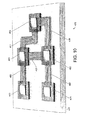
図3は、本発明の1実施形態によるダイレクトコネクト信号システム200を示している。信号システム200は、1対の集積回路パッケージ201Aおよび201B(これらは、“集積回路デバイス”とも呼ぶ)を備え、これらは、プリント回路ボード205に装着しまたダイレクトコネクト・ケーブル203を介して互いに結合されている。図示のように、ダイレクトコネクト・ケーブル203は、集積回路パッケージ201の各々に固着され、そしてプリント回路ボード205より上に持ち上げられた形式で延在している。すなわち、ケーブル203は、プリント回路ボード205より上の空中に浮遊させ、これにより、トレースまたはプリント回路ボード205内の他の導電性構造を通らずに、集積回路パッケージ201間で高速信号の伝送を可能にする。この構成により、プリント回路ボードの入口および出口の構造(例えば、導電性ビア等)から生ずる寄生容量および信号反射が回避される。さらに、ダイレクトコネクト・ケーブル203が1組の同一長さの導体で構成することができるため、プリント回路ボード205を通る信号経路の異なった長さから生ずるタイミング・スキューも、回避される。尚、ダイレクトコネクト・ケーブル203は、図3においては、集積回路パッケージ201への接続部によってのみ支持されるものとして示したが、1つ以上の機械的な支持部を、オプションとして、ケーブル203の下に配置するようにすることもできる。
The invention will now be described by way of example and not limitation with reference to the accompanying drawings. In the drawings, the same reference numerals are used to refer to similar elements.
FIG. 3 illustrates a direct
図3のこの実施形態では、集積回路パッケージ201の各々は、フリップチップ・パッケージであって、これは、基板219の上面に対しパッド側を下にして装着した集積回路ダイ217を備えている。集積回路ダイ217は、オプションとして、非導電性のハウジング215(例えば、セラミックまたはポリマー材料により形成されたもの)にカプセル封入するようにもできる。基板219の上面のダイ217またはハウジング215により覆われていない部分は、露出された領域を構成し、そしてこの領域に対し、1つ以上のダイレクトコネクト・ケーブル203を取り付けることもできる。したがって、この基板219の下側にある回路ボード・コンタクト221へ基板219を通して高速信号をルーティングするのではなく、導電性トレース209は、基板219の上面に配置し、そして高速I/Oパッド225(すなわち、ダイ217上に形成された高速入出力(I/O)回路に結合される、集積回路ダイ217上のパッド)と基板219の上記露出領域との間でルーティングする。コネクタ207を使うことにより、ダイレクトコネクト・ケーブル内の電気信号導体(すなわち、電流を運ぶことができる導体)を導電性トレース209に対し、恒久的に結合するかあるいは除去可能に結合する。この構成により、基板層219内の信号再分配により生ずる寄生容量、信号反射およびタイミング・スキューは、回避される。
In this embodiment of FIG. 3, each of the
続いて図3を参照すると、電源電圧と低速信号(すなわち、高いデータ・スループットを当てにしない信号)は、在来のルーティング技法(例えば、図3に示す部分的入口ビア223およびPCBトレース224等)を使って、パッケージ基板219およびプリント回路ボード205中をルーティングするようにできる。かなりの数のチップ−チップ間接続は、ダイレクトコネクト・ケーブル203により果たすことができるため、パッケージ基板219およびプリント回路ボード200内の信号ルーティングは、実質上密集度が低くなり、これにより基板およびプリント回路ボードの層の数を減少させるのを可能にする。また、パッケージ基板219およびプリント回路ボード205を通してスキュー・トレラントの信号のみ(目的地に対し他の信号と特定の位相関係で到達することが必要でない信号))をルーティングすることにより、パッケージ基板219およびプリント回路ボード205内における信号経路長を等しくするのに使用される、蛇行ルーティング技法およびその他の技法は不要となり、これによりさらに、ルーティング密集を軽減し、パッケージ基板219およびプリント回路ボード205の接続を簡単化する。1実施形態においては、すべての信号またはほぼすべての信号を、1つ以上のダイレクトコネクト・ケーブル203を介してルーティングし、電源電圧(例えば、電力とグランド)および無視できる数の信号(またはゼロ信号)をプリント回路ボード205およびパッケージ基板219内の導電性構造を介して分配する。このような実施形態では、プリント回路ボード205およびパッケージ基板219の一方または双方は、幾つかの基板層のみあるいは単一の層のみをもつ単純な構造へと変えることもできる。
With continued reference to FIG. 3, the power supply voltage and low speed signals (ie, signals that do not rely on high data throughput) can be achieved using conventional routing techniques (eg, partial entry via 223 and
図3を再考すると、注目すべきことは、ダイレクトコネクト信号システム200を実現するためにはプリント回路ボード205に何等変更を要しない点である。このため、設計者が、多数の在来ルーティングの信号経路をもつシステム(すなわち、回路ボード貫通ルーティング形システム(through-circuit-board-routed systems)を、図3のダイレクトコネクト信号ルーティングをもつシステムに移したいとき、このような移しは、ボード・レベルでの変更を必要とせずに、一時に1つの信号経路で実現することもできる。在来のルーティングのためのプリント回路ボード上のトレースは、単に、接続しないままに残しておき、そしてその代わりにダイレクトコネクト・ケーブルで高速信号経路を提供するようにできる。このシステム内の各信号経路(あるいは1グループの信号経路)は、ダイレクトコネクト・信号配置にうまく移されるため、プリント回路ボードの製作は、それら痕跡的なトレースを省くことによって簡略化することもできる。
Reconsidering FIG. 3, it should be noted that no changes are required to the printed circuit board 205 in order to realize the direct
ダイレクトコネクト信号システム200のさらに別の利点は、集積回路パッケージ201のいずれかと高速テスタ(図示せず)との間のダイレクトコネクト・ケーブル接続を通して、高速テスト(“ACテスト”としても知られている)を実行することができることである。後でさらに詳細に説明するが、ダイレクトコネクト・ケーブル接続を通しての集積回路パッケージ201の高速テストは、3状態デバイス201Bに対する必要性を除去し、そしてプリント回路ボード205上のプローブ用トレースから通常生ずる寄生容量および信号反射が回避される。
Yet another advantage of the direct
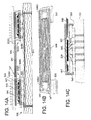
図4Aは、図3の集積回路パッケージ201Aの上面図であり、ハウジング215および集積回路ダイ217の一部を透明にして、パッケージ基板219上に配置されたダイ・パッド225(または集積回路ダイ217上に形成されたバンプまたはその他のタイプのコンタクト)と導電性トレース209を露出させてある。1実施形態においては、導電性トレース209の全長は、基板219の表面に沿って、ダイ・パッドのあるコンタクト(これらは、スプリング・タイプのコンタクト、粒子インターコネクト、または他の高密度のインターコネクト構造により確立することができる)からパッケージ基板219のその露出領域上のコンタクト・ゾーン231へと延在している。以下で説明する代替の実施形態においては、トレース209は、基板219の下側(すなわち装着側)または基板219の内部層上に沿って、全体または部分的に延在させることができる。
4A is a top view of the
このトレース209は、コンタクト・ゾーン231において、例えばダイレクトコネクト・ケーブルからのコンタクトを受けるのに適合させた高密度ランドにおいて終了する。代替的には、トレース209は、ダイレクトコネクト・ケーブルの一体的コンポーネントを形成するため、基板219を超えて延在することができる。また、図4Bおよび図4Cに示すように、追加のコンタクト・ゾーン(すなわち、図4Bのゾーン247および249、図4Cのゾーン267A−267D)を設けることができ、これにより、多数のダイレクトコネクト・ケーブルへの接続ができるようにしたり、あるいは集積回路ダイ217の反対側および隣接する側の一方または双方におけるパッケージ基板の露出領域に接触するため単一のダイレクトコネクト・ケーブルへの接続ができるようにしたりする。また、トレース209のうちの1つ以上のものに、共通のダイ・コンタクトから異なったコンタクト・ゾーンへ延在する2以上のトレース・セグメントを含ませることもできる。例えば、図4Bを参照すると、トレース250は、トレース・セグメント251Aを含み、これは、ダイ・コンタクト245からコンタクト・ゾーン249へ延在し、そして別のトレース・セグメント251Bは、ダイ・コンタクトからコンタクト・ゾーン247へと延在している。以下で説明するが、このような多セグメントのトレースは、任意の数の集積回路パッケージへの高速の多ドロップ形接続(例えば多数のドロップ・バス)を確立するために使用することができる。
This
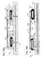
図5Aは、図3の集積回路パッケージ201Aおよび201B並びにダイレクトコネクト・ケーブル203の上面図である。各集積回路パッケージ201のハウジングおよび集積回路ダイは、透明にして、パッケージ基板上に配置したダイ・パッド225およびトレース209を露出させてある。図示した実施形態においては、ダイレクトコネクト・ケーブル203は、リボン・スタイルのケーブルであって、フレキシブルで低ロスの誘電体材料293内にコプレーナ配列で配置した1組の電気信号導体297を備えている。ケーブル・コネクタ207A、207Bを使用することにより、電気信号導体297とパッケージ基板219Aおよび219Bのそれぞれの上に配置したトレース209との間に接続を確立する。1つのシートまたはウェブの導電性材料(図示せず)は、シールド目的(例えば、グランドまたは他の基準電圧への接続により)のため、導体297の上または下に配置することができ、これにより、マイクロ・ストリップライン・ケーブルを実現する。代替的には、導電性のシートまたはウェブを、導体297の上および下の両方に配置することができ、これによって、コプレーナのストリップライン・ケーブルを形成する。また、代替的には、電気信号導体297それ自体を信号とグランドに結合することもでき、これにより、隣接する信号間のクロストークを低減する。さらに、図5Bに示すように、ダイレクトコネクト・ケーブル310内の導体311A,311Bの対を撚り線対構成(例えば、互いに他方の上に交差させるが、絶縁材料で分離)に配置することもでき、これにより、誘導性結合を低減することができる。2つより多い導体を互いに撚ることは、さらに別の実施形態で行うこともできる。また、コプレーナ構造ではなく、それら導体を、同軸構成または他の3次元構造で配置することもできる。さらに、ダイレクトコネクト・ケーブルは好ましくはフレキシブルにすることによって広範なインターコネクト距離および集積回路トポロジーを許容するようにしているが、リジッドな相互接続構造を使用することもできる。図5Aおよび図5Bには単一平面の導体を示しているが、多数の平面の導体をケーブル203および310内に形成することもでき、このとき、各平面は、絶縁層により、オプションとしてはシールド層により隣接する平面から分離する。
5A is a top view of
図6は、代表的なコンタクト・トポロジーを示しており、そしてこれは、集積回路パッケージ201の基板上に配置したトレースと、ダイレクトコネクト・ケーブル203内の導体297との間に電気的接続を確立するために使用することができる。詳細図337Aにおいては、導電性スプールまたは樹枝状コンタクト343を、パッケージ基板209上に配置した各々のトレース209に対しハンダ付けしたり、形成したりあるいはその他の方法で固着したりでき、そしてそれらは、ダイレクトコネクト・ケーブル203内の対応する導体297を突き刺すことにより電気的接続を確立するために使用することができる。また逆に、詳細図337Bに示すように、スプールまたは樹枝状コンタクト353をダイレクトコネクト・ケーブル導体297に固着することができ、そしてこれらは、対応する基板トレース209を突き刺すことによって電気的接続を確立するために使用することもできる。
FIG. 6 shows a typical contact topology, which establishes an electrical connection between traces placed on the substrate of the
再び詳細図337Aを参照するが、コネクタ207を使用することにより、ダイレクトコネクト・ケーブルをパッケージ基板219の露出領域に結合する。また、描いた実施形態では、ダイレクトコネクト・ケーブルは、導体297の上と下に配置した絶縁層351および352と、絶縁層351の上に配置したシールド層349を備えている。上述のように、追加のシールド層を絶縁層352の下に配置することができ、これにより、ストリップラインまたはコプレーナのストリップライン・ケーブルを形成することができる。
Referring again to detail
別の実施形態においては、詳細図337Cに示したように、基板トレース209に固着したフィンガ状の突出要素357を使用することにより、ケーブル導体297と電気的コンタクトをつくる。突出要素357は、好ましくは、弾性のスプリング状の材料から製作し、そしてこれは、ダイレクトコネクト・ケーブル203を基板に固着する際に導体297に対し偏倚させる。但し、他のタイプの材料も使用することができる。詳細図337Dに示すように、フィンガ状の突出要素361は、代替的には、ダイレクトコネクト・ケーブル297に固着することができ、そしてダイレクトコネクト・ケーブル203を基板に接続するときに基板トレース209に対し付勢することもできる。詳細図337Eは、さらに別の実施形態を示しており、これでは、基板トレース209に固着したあるいはそれに対し一体的に形成したポイント・コンタクト365を使用して、ダイレクトコネクト・ケーブル203内の対応する導体297と接触する。詳細図337Fを参照すると、ポイント・コンタクト369を代替的にはケーブル導体297の端部に固着するかあるいは一体的に形成し、そしてこれを使用して基板トレース209と接触する。種々の他の構造も使用でき、これにより、他の実施形態においてダイレクトコネクト・ケーブル203の導体297と基板トレース209との間に電気的接続を確立することができ、そしてこれは、ハンダ・ジョイント、スプリング・スタイルのコンタクト、オス対メスの接続構造、粒子インターコネクト構造等(これらに限定しない)を含む。より一般的には、本発明の要旨および範囲から逸脱することなく、任意の構造または技術を使用することができ、これによりダイレクトコネクト・ケーブル203の導体297を、基板219上にあるいはその中に配意した対応するコンタクトに接続することができる。
In another embodiment, electrical contact is made with
図7は、1組の集積回路パッケージ391,392および393を示しており、これらは、2つのダイレクトコネクト・ケーブル203Aおよび203Bを介して結合されて、多ドロップの信号システム390を確立する。集積回路パッケージ392を参照すると、基板トレースの各々は、1対のトレース・セグメント399Aおよび399Bを含んでいて、反対のコンタクト・ゾーンまで延在している。したがって、集積回路パッケージ392のこの多セグメントの基板トレース(これは、本文ではブリッジ集積回路パッケージ(“ブリッジIC”)と呼ぶ)は、ダイレクトコネクト・ケーブル203Aと203Bとの間のブリッジを形成し、そして一緒になると、ダイレクトコネクト・ケーブル203Aおよび203Bの導体と集積回路パッケージ392の多セグメント・トレースとは、集積回路パッケージ391,392および393の各々間の連続した信号経路を形成する。この信号経路は、集積回路パッケージ392のダイ・パッドに対し、回路ボード・ルーティング形信号経路において通常存在する長いスタブ接続なしで、接触し、多くの多ドロップ形信号システムを悩ます寄生容量および信号反射は実質的に低減される。尚、任意の数のブリッジ用ICを信号システム390に含めることもできる。また、ブリッジIC392は、図示した反対側のエッジ上ではなく、隣接するエッジ上のダイレクトコネクト・コンタクト・ゾーンを含むこともできる。信号システム390は、マスタ/スレーブ・システム(この場合、スレーブ・デバイスは、マスタ・デバイス(例えば、メモリ・コントローラとスレーブ・メモリ・デバイス)からのコマンドまたは要求に応答してダイレクトコネクト・信号経路へ信号を駆動する)としたり、ピア・ツー・ピアの信号システム(この場合、集積回路パッケージのうちの任意のもの(またはその部分集合)が、信号経路の制御を得て、それ自身の意志に基づいて信号経路へ信号を出力する)としたり、もしくは、多ドロップ形動作が望まれる任意の他の信号システムとしたりできる。他の実施形態においては、ブリッジIC392は、2つより多いダイレクトコネクト・コンタクト・ゾーンを含むことができ(各コンタクト・ゾーンに延在する1組のトレース・セグメントを伴う)、これにより、1つより多い多ドロップ形信号経路がブリッジIC392により確立されるのを可能にしたり、あるいはブリッジIC392がハブ・デバイスを構成するスター・トポロジーを可能にしたりするようにできる。
FIG. 7 shows a set of integrated circuit packages 391, 392, and 393 that are coupled via two
図8は、代替のダイレクトコネクト信号システム405を示しており、これは、多ドロップ形信号経路を確立するのに使用する。パッケージ基板上の多セグメント・トレースを通して多ドロップ形ルーティングを確立するのではなく、2組の導体415Aおよび415Bをダイレクトコネクト・ケーブル・アセンブリ412内に設け、そして各組の導体は、中間の集積回路パッケージ406と、エンド・ポイントの集積回路パッケージ407,408のそれぞれとの間に結合する。組415Aの導体は、組415Bの導体にそれぞれ結合して、エンド・ポイントのパッケージ407,408間に延在する多ドロップ信号経路を確立し、また中間パッケージ406に結合される。1実施形態においては、それら導体組は、コネクタ418内で互いに結合(例えば、ハンダ・ジョイント、圧力コンタクトまたは他の導電性結合を介して接続)することにより、各対の導体間にYジョイント414を形成する。代替の実施形態においては、導体415A,415Bは、コネクタ418においてではなく、それらの長さに沿った点において互いに結合することもできる。また、代替の実施形態では、2つより多い組の導体をダイレクトコネクト・ケーブル・アセンブリ412内に含めることができ、そして互いに結合することによって、任意の数の追加の中間集積回路パッケージに対する接続を(例えば、各々の追加の中間集積回路パッケージにおいてYジョイント414を使用することにより)可能にすることができる。
FIG. 8 shows an alternative direct
図9は、スター・タイプのインターコネクト・トポロジー430を示しており、これは、図8の1対のダイレクトコネクト・ケーブル・アセンブリ(すなわち、アセンブリ412Aおよび412Bと図7のブリッジIC392とを使用して実現する。ブリッジIC392は、スター・トポロジーのハブ・デバイスを構成し、そしてこれは、エンド・ポイントの集積回路パッケージ431,432,433および434の各々に結合する。このため、図7,図8および図9の例から見られるように、事実上任意の高速のインターコネクト・トポロジーを、図6および図7で説明したダイレクトコネクト・ケーブル・アセンブリおよびブリッジICの一方または双方を使用して実現することができる。
FIG. 9 shows a star
図10は、ダイレクトコネクト信号経路485,487,489,491,493の例示の配置を示しており、これらは、プリント回路ボード477上の装着した多数の集積回路パッケージ(478,480,481および482)の間に確立する。種々の他のコンポーネント(図示せず)も、プリント回路ボード477に装着し、そして在来の相互接続構造を使用してまたは追加のダイレクトコネクト・ケーブルを使用して、互いに相互接続したりあるいは集積回路パッケージ478−482へ相互接続したりまたはその双方を行うようにすることができる。図示したように、集積回路パッケージ478−482間に信号経路を確立するのに使用するそれらダイレクトコネクト・ケーブルは、直線のケーブル485,487および493、Sタイプのケーブル491およびエルボー形ケーブル489を含んでいる。任意の他の数の湾曲部または形状をもつケーブルも、使用することができる。また、コプレーナのケーブルを図示したが、他のケーブル幾何形状を使用することもできる(例えば、同軸ケーブル)。集積回路パッケージ481は、ブリッジICとして、ダイレクトコネクト・ケーブル485,491および493のすべてまたはその1対間にスルー接続を確立することができる。代替的には、ダイレクトコネクト・ケーブル485,491および493は、各々、集積回路パッケージ481内の別個の組のI/O回路に結合することもできる。集積回路パッケージ480および482は、同様にブリッジICとすることによって、ダイレクトコネクト・ケーブル間にスルー接続を確立することもできる。尚、集積回路パッケージ間の高速のシグナリングが必要とされる事実上任意のタイプのシステムに対し、図10に示したダイレクトコネクト信号経路を適用したり、あるいは適用のため修正することができる。例えば、データ処理システムにおける集積回路パッケージ間(例えば、汎用または専用のプロセッサと対応するチップセット・コンポーネントまたは特定用途向け集積回路との間、またはメモリ・コントローラとメモリ・デバイスおよびメモリ・モジュールの一方または双方との間)、ネットワーク・スイッチング・システム間の集積回路パッケージ間(例えば、1つ意序のライン・カード、スイッチ・ファブリック・カード等上の集積回路パッケージ間)、高速データ多重化システム等の集積回路パッケージ間において、ダイレクトコネクト・ケーブルを使用して接続を確立することができる。
FIG. 10 shows an exemplary arrangement of direct
図11は、本発明の代替の実施形態によるダイレクトコネクト信号システム500を示している。信号システム500は、1対の集積回路パッケージ501Aおよび501Bを備えており、これらは、プリント回路ボード507に装着され、そしてダイレクトコネクト・ケーブル503を介して互いに結合されている。図3のダイレクトコネクト・ケーブル203とは対照的に、ダイレクトコネクト・ケーブル503は、両端にコネクタを含んでおらず、むしろ集積回路パッケージ501Aの一体的なコンポーネントである。図示の実施形態では、ダイレクトコネクト・ケーブル503は、パッケージ基板509のエッジ(例えば、パッケージ基板509の上側表面と下側表面との間に形成された凹部)内に受け、そしてダイレクトコネクト・ケーブル503の電気信号導体502は、基板509内を(例えば、基板の内部の層の表面に沿って)延在することにより、集積回路ダイ512に結合された1組のビア504またはその他の導電性構造に接触する。代替的には、ダイレクトコネクト・ケーブル503の導体502は、パッケージ基板509の上面に沿って延在することができ、これにより、ダイ512に直接接触することもできる(ビア504を不要にする)。さらに別の実施形態では、ダイレクトコネクト・ケーブル503の導体502は、パッケージ基板509の底面に沿って延在し、そしてパッケージ基板509内に配置したビアまたはその他の導電性構造を通してダイ512と接触するようにできる。図3のダイレクトコネクト・ケーブル203の場合と同じように、ダイレクトコネクト・ケーブル503は、フレキシブルあるいはリジッドのものとしたりでき、またマイクロ・ストリップライン(すなわち、導電性シールド506を有する)、コプレーナのストリップライン、あるいは非コプレーナのケーブル(例えば、同軸またはその他の非コプレーナの構成)とすることもできる。
FIG. 11 illustrates a direct
図12は、信号システム実施形態510を示しており、これは、集積回路パッケージ511A,511Bを備えていて、これらは、プリント回路ボード517に装着され、そして各々、一体的なダイレクトコネクト・ケーブル514A,514Bを有し、これらは、それぞれ中間スパン・コネクタ515A,515Bにおいて終端している。1実施形態においては、中間スパン・コネクタ515A,515Bは、互いに異なっており、そして中間スパン・コネクタ515Aは、中間スパン・コネクタ515Bの突出コンタクトを受けるように構成されている(すなわち、オス/メス・コネクタ対)。代替の実施形態においては、中間スパン・コネクタ515A,515Bは、互いに同一のものであり、そしてこれらは、ラッチ構造を含むことによって、ケーブル514A,514B内のそれぞれの組の導体を、互いに整列したコンタクト状態で維持する。中間スパン・コネクタ515A,515Bは、恒久的にあるいは取り外し可能に互いに結合するようにすることができる。図11の実施形態と同じように、ダイレクトコネクト・ケーブル514A,514Bの一方または両方における導体は、全体的にあるいは部分的に、対応するパッケージ基板内において延在するようにしたり(図示)、あるいはそのいずれかの表面上で延在するようにしたりできる。また、ダイレクトコネクト・ケーブル514A,514Bは、フレキシブルあるいはリジッドのものとしたりでき、またマイクロ・ストリップライン(すなわち、導電性シールド506を有する)、コプレーナのストリップライン、あるいは非コプレーナのケーブルとすることもできる。
FIG. 12 shows a
図13は、本発明の別の実施形態によるダイレクトコネクト信号システム512を示している。信号システム512は、集積回路パッケージ522A,522Bを含んでおり、これらは、互いにダイレクトコネクト・ケーブル523を介して結合されており、そしてこのケーブルは、その長さの全体あるいは一部に沿ってプリント回路ボード527上に載置されている。ダイレクトコネクト・ケーブル523は、好ましくは、コプレーナの構造のものであって、複数の並列の導体を有しているが、しかしこれは、代替的には、同軸または他の非コプレーナのケーブルとすることもできる。また、このダイレクトコネクト・ケーブルの導体525は、パッケージ基板526の下側にあるランド524Aまたは他の導電性の構造に直接接触したり、あるいは、図13に示したように、在来のインターコネクト構造、例えばコンタクト・ボール528(例えば、BGAのコンタクト・ボール)、コンタクト・スプリング等によって集積回路パッケージに結合するようにしたりできる。この構成により、ダイレクトコネクト・ケーブル523を従来通りに製作された集積回路パッケージ(図13に示したフリップチップ・パッケージ522A,522B、またはダイレクトコネクト・ケーブル523内の導体と接触するためのリードまたは他のコンタクトを有する集積回路パッケージ)と共に使用することができる。集積回路パッケージ内の信号再分配に関連する上述の問題は、図13の実施形態では依然として存在することがあるが、PCBルーティングに関連する寄生容量、信号反射および信号スキューは、相当低減され、これによって、より高い信号レートを可能にし、プリント回路ボード527におけるルーティング密集を軽減することができる。ダイレクトコネクト・ケーブル523の導体525は、好ましくは、低ロスの誘電体材料の層529によってプリント回路ボードから電気的に分離され、これにより、プリント回路ボード527の上面上にプリントされたあるいは他の方法で形成された導電性トレースを、ケーブルの下側でルーティングできるようにする。図3、図9および図10を参照して上述したダイレクトコネクト・ケーブルの場合と同じように、ダイレクトコネクト・ケーブル523は、好ましくは、フレキシブルのものとし、これによりこのケーブルが、プリント回路ボード527に装着された他のコンポーネント(例えば、集積回路パッケージ522A,522Bの間に配置された他の集積回路デバイスまたは回路コンポーネント)の上へそしてその上(及び/またはその周り)をルーティングできるようにする。代替的には、ダイレクトコネクト・ケーブル523は、リジッドのものとすることもできる。また、ダイレクトコネクト・ケーブル523は、システム・アセンブリの間にプリント回路ボード527に固着したり(例えば、接着剤または締結部材を使用)、あるいはプリント回路ボード527上に固着せずに載置されるようにしたりできる。
FIG. 13 illustrates a direct
図14A〜図14Cは、本発明の別の実施形態によるダイレクトコネクト信号システム530を示している。先ず、図14Aを参照すると、ダイレクトコネクト・ケーブル546は、回路ボード531に装着された集積回路パッケージ533A,533Bの間に延在し、そしてこれは、リッド・コンポーネント535A,535Bのぞれぞれの1つにより各パッケージ533に固着されている。1実施形態においては、スプリング・タイプのコンタクト537は、ダイレクトコネクト・ケーブル546から延在して、パッケージ基板549A,549Bの表面に配置されたトレースと接触する(例えば、図4A〜図4Cで説明したのと同じ)。他のケーブル−パッケージ相互接続の構造および技術は、代替の実施形態において使用することもでき、その代替の実施形態では、限定する訳ではないが、図6で上述したコンタクトの構造および技術を含んでいる。図14Aの実施形態においては、リッド・コンポーネント549は、熱伝導材料から形成され、そしてこれは、パッケージ・ハウジング544の上面と接触した状態で配置されたヒート・シンク構造541(例えば、フィン)を含んでいる。熱伝導性材料539(または接着剤)を使用することもでき、これによって、集積回路パッケージ533からリッド・コンポーネント535への熱伝導を向上させることができる。
14A-14C illustrate a direct
1実施形態においては、図14Bに示したように、ダイレクトコネクト・ケーブル546の個々の導体547は、集積回路ダイ・ハウジング544にしたがってサイズを決めたケーブル546内の開口548A,548Bの周囲にルーティングし、これによって、パッケージ・ハウジング544とリッド・コンポーネント535との間のより直接的な接続を可能にする。代替的には、その開口を省略し、そして導体547を、パッケージ・ハウジングの上面の上に直接ルーティングするようにすることもできる。ヒート・シンク構造541は、リッド・コンポーネント535と区別したものとしたり、あるいは代替の実施形態においては、それらを一緒に省略することができ(例えば、図14Bの551で示す)、そしてリッド・コンポーネント535を、熱伝導性材料以外の材料から形成するようにすることもできる。
In one embodiment, as shown in FIG. 14B,
図14Aの実施形態においては、リッド・コンポーネント535は、突出部材543を含み、これは、パッケージ基板549内の対応する孔またはスロット内へ延在することにより、リッド・コンポーネント535を基板549に固定する。図14Cを参照すると、リッド・コンポーネント561は、代替的には、パッケージ基板549に部材563によって固着することもでき、そして部材563は、パッケージ基板549の外側エッジに周りにスナップして、リッド・コンポーネント561を基板549の上側表面および下側表面に対し固着する。このような実施形態においては、ハウジングを省略し、そして熱伝導材料を、集積回路ダイ545とリッド・コンポーネント561との間に直接配置するようにすることもできる。詳しくは、リッド561(または535)とダイレクトコネクト・ケーブル546を集積回路パッケージ533に固着するための任意の機構または材料を、本発明の要旨および範囲から逸脱せずに使用することもできる。
In the embodiment of FIG. 14A, the
図15Aおよび図15Bは、本発明の別の実施形態によるダイレクトコネクト信号システム580を示している。ディスクリートのダイレクトコネクト・ケーブルではなく、ダイレクトコネクト信号経路587A−587Gをスーパー構造585内に配置し、このスーパー構造585は、プリント回路ボード581に対し、集積回路パッケージ583A〜583Nの上面の上で装着されている(尚、図15Bのプロファイル図では、ダイレクトコネクト信号経路587Aおよび587Bのみを示している)。図15Bの実施形態においては、ポスト591は、プリント回路ボード581に固着され、またスーパー構造585の孔594内に受けられて、これにより、スーパー構造585とプリント回路ボード581を整列させる。その他の整列技術も、代替の実施形態においては使用することができる。
15A and 15B illustrate a direct
ダイレクトコネクト信号経路587は、スーパー構造585上にプリントしたまたはその他の方法で配置した導電性トレースにより形成したり、あるいは、図3〜図14で説明したダイレクトコネクト・ケーブルの1つまたはそれ以上をスーパー構造585の表面上に固着することにより形成することもできる。いずれの場合でも、コンタクト構造589を設けることによって、ダイレクトコネクト信号経路の端子592と、集積回路パッケージ583の基板上に配置されたコンタクトとの間にコンタクトを確立する。図15Bにおいては、コンタクト構造589を、突出フィンガ・タイプのコンタクトとして示したが、他のタイプのコンタクト構造も使用することができ、それには、限定する訳ではないが、図6で説明したコンタクト構造が含まれる。図15Aを参照すると、これら分かるように、ダイレクトコネクト信号経路587A〜587Gは、多ドロップ信号構造487Dおよび587Eだけでなく、集積回路パッケージ間のポイント・ツー・ポイントのリンク587A,587B,587C,587Fおよび587Gを形成することができる。多ドロップ構造587Eを特に参照すると、分かるように、コンタクト領域599は、信号経路587Eの長さに沿った1点において配置され(すなわち、両端とは異なる)、これにより、コンタクト領域599内の各コンタクトからコンタクト構造589とパッケージ基板トレースとの組み合わさった長さまで延在するスタブを制限する。尚、このような中間スパン・コンタクトは、本文に記述した他のダイレクトコネクト・ケーブルと共に使用することができ、これにより、図7で説明したブリッジIC382あるいは図8で説明したケーブル・アセンブリ412を必要とせずに、多ドロップ信号経路を確立することができる。また、ダイレクトコネクト・信号経路587A〜587Gのコンタクトと集積回路パッケージ583上の対応するコンタクトとの間に細かな配列を容易にするため、アパーチャを、スーパー構造585においてコンタクト・ポイント592の上に設けることもできる。
The direct connect signal path 587 may be formed by conductive traces printed or otherwise disposed on the
図16Aおよび図16Bは、ダイレクトコネクト信号システム610,625をそれぞれ示しており、これらは、図3および図9〜図12に示したフリップチップ・パッケージではなくあるいはそれらフリップチップ・パッケージと組み合わせて、リード付きの集積回路パッケージを含んでいる。図16Aを参照すると、ダイレクトコネクト・ケーブル617は、リード付き集積回路パッケージ613および645の上を延在し、そしてソケット614および616により集積回路パッケージに固着されている。すなわち、ソケット614は、集積回路パッケージ613の周りに配置し、そしてこれは、導電性部材618Aを含んでいて、この部材は、それぞれのケーブル接続ポイント612Aから集積回路パッケージ613の対応するリード621まで延在している。同様に、ソケット616は、集積回路パッケージ615の周りに配置し、そしてこれは、導電性部材618Bを含んでいて、この部材は、それぞれのケーブル接続ポイント612Bから集積回路パッケージ615の対応するリード622まで延在している。ケーブル内の導体619A〜619Nは、導電性部材618をもつ各対のコンタクト620間に延在する。上述のダイレクトコネクト・ケーブルの場合と同じように、ダイレクトコネクト・ケーブル617は、好ましくは、フレキシブルのものとして、集積回路パッケージ613および615が互いに異なった異なった位置および向きで配置されるときに、これらパッケージの相互接続を可能にする。代替的には、ダイレクトコネクト・ケーブル617は、リジッドのものとすることもできる。また、このダイレクトコネクト・ケーブルは、マイクロ・ストリップライン、コプレーナのストリップライン、あるいは非コプレーナのケーブルとすることもできる。最後に、集積回路パッケージ613および615は、ガルウィング・リード付きまたはJリード付きのパッケージとして図示したが、他のタイプのリードをもつパッケージを代替の実施形態において使用することもできる。
FIGS. 16A and 16B show direct
図16Bにおいて、ダイレクトコネクト・ケーブル635を使用することにより、フリップチップ集積回路パッケージ626とリード付きパッケージ627とを相互接続する。フリップチップ・パッケージ626は、概して図3を参照して説明したように実現し、そして導電性トレース629は、パッケージ基板628の表面に沿ってルーティングして、基板628の露出した領域にあるゾーンに接触させる。導電性構造630は、トレース629と接触する状態で配置し、そしてこれは、このパッケージ・ハウジングの表面に沿ってこのハウジングの上面まで延在する。コンタクト631(例えば、ハンダ・ボールまたはその他の構造)を設けることにより、構造630とダイレクトコネクト・ケーブル635の導体632A〜632Nとの間の電気的接続を行う。リード付きパッケージ627では、導電性構造642は、同様にパッケージ・リード641からパッケージ・ハウジングの上面へ延在し、そしてその上面で、コンタクト643を使用してダイレクトコネクト・ケーブル635の導体632A〜632Nとの電気的接続を行う。代替の実施形態においては、フリップチップ・パッケージ626は、図3〜図14で上述した接続技術および構造の任意のものを使用して、ダイレクトコネクト・ケーブル635に結合することもできる。同様に、リード付きパッケージ627は、図16Aで説明したソケット構成を使用してダイレクトコネクト・ケーブル635に結合することもできる。さらに、図15Aおよび図15Bで説明したダイレクトコネクト・スーパー構造585は、図16Aおよび図16Bに示したディスクリートのダイレクトコネクト・ケーブル617および635の代わりに使用することもできる。
In FIG. 16B, the
図17A〜図17Fは、追加のダイレクトコネクト信号システムの実施形態を示している。先ず図17Aを参照すると、集積回路パッケージ653および657は、別個のプリント回路ボード651および655にそれぞれ装着しており、そしてダイレクトコネクト・ケーブル659を介して互いに結合している。プリント回路ボード651および655は、互いに任意に位置決めし、そして任意の許容可能なシグナリング距離で分離するようにすることができる。プリント回路ボード651および655は、追加の集積回路パッケージを有することができ、そしてこれらは、1つ以上の他のダイレクトコネクト・ケーブルを通して互いに結合するか、あるいは図7で説明した多ドロップ構成で結合することができる。また、ダイレクトコネクト・ケーブル659は、図8で説明した多数の組の導体を含むことができ、これにより、それら2つのプリント回路ボード651および655上の多数の集積回路パッケージの相互接続を可能にする。
17A-17F illustrate additional direct connect signaling system embodiments. Referring first to FIG. 17A, integrated
図17Bは、ダイレクトコネクト信号システムを示しており、これにおいては、マザーボードまたはバックプレーン661上に装着された集積回路パッケージ663は、ドーターボード665上に装着した集積回路パッケージ667に対しダイレクトコネクト・ケーブル669を介して結合する(すなわち、プリント回路ボードは、マザーボードに対しコネクタ670または類似の構造を介して取り外し可能に結合される)。図17Cは、別のダイレクトコネクト信号システムを示しており、これにおいては、集積回路パッケージ678および682は、それぞれのドーターボード676および680に装着され、またダイレクトコネクト・ケーブル684を介して互いに結合されている。ドーターボード676および680は、バックプレーンまたはマザーボード675のそれぞれのコネクタ684および686内へ取り外し可能に挿入される。図17Bおよび図17Cの信号システムの例示的な応用例には、これに限定する訳ではないが、ネットワーク・スイッチング装置(例えば、スイッチまたはルータ)内のバックプレーンに挿入されるライン・カードまたは他のカード、コンピューティング・デバイスまたはコンシューマ電子デバイス等のマザーボードまたはバックプレーンに挿入されるメモリ・モジュールが含まれる。
FIG. 17B illustrates a direct connect signaling system in which an
図17Dは、さらに別のダイレクトコネクト信号システムを示しており、これにおいて、集積回路パッケージ697および699は、プリント回路ボード695または他の基板の対向する側に装着し、そしてこれらは、ダイレクトコネクト・ケーブル700を介して互いに結合する。図17Aの信号システムの場合と同じように、図17B〜図14Dで示した実施形態の各々は、ダイレクトコネクト・ケーブルで互いに結合した追加の集積回路パッケージを含むことができ、また、ダイレクトコネクト・ケーブル669,684および700は、図7で説明した多数の組のコネクタを含むことができ、これによって多数の集積回路パッケージの相互接続を可能にすることができる。
FIG. 17D shows yet another direct connect signaling system in which
図17Eは、本発明の別の実施形態による信号システム710を示している。信号システム710は、第1の集積回路パッケージ712を含み、これは、プリント回路ボード711に装着され、そしてボンド・ワイヤ715または他のコンタクト構造を介してダイレクトコネクト・ケーブル・アセンブリ717の導体に結合されている。その他のボンド・ワイヤを使用することもでき、これにより、集積回路パッケージ712の下面上のハンダ・ボールまたは他のコンタクトに対し、集積回路ダイを結合することができる。ダイレクトコネクト・ケーブル・アセンブリ717は、締結部材716をもつリッド・コンポーネント714を含み、これにより、このアセンブリ717を集積回路パッケージ712に固着する。また、このダイレクトコネクト・ケーブル・アセンブリは、コネクタ719を含み、これにより、ケーブル・アセンブリ717の遠い方の端部を別のプリント回路ボード721に固着し、またケーブル・アセンブリ717の導体をプリント回路ボード721上に配置したトレースに結合する。このプリント回路ボード・トレースは、別の集積回路パッケージ723のリード(または他のコンタクト)に結合し、これにより、集積回路パッケージ712と723との間の高速信号経路を完成させる。このように、システム710の高速信号経路全体は、ハイブリッド経路であって、集積回路パッケージ712へのダイレクトコネクト・ケーブル接続と、集積回路パッケージ723への在来の接続とを有している。ケーブル−ボード・コネクタ719は、プリント回路ボード721に対し恒久的にあるいは取り外し可能に結合することができる。
FIG. 17E illustrates a
引き続き図17Eを参照すると、理解されるべきであるが、集積回路パッケージ712は、代替的には、図3〜図13で説明したタイプの集積回路パッケージのうちの任意のものとすることができ、また図3〜図13で説明したケーブル接続のうちの任意のものを有するようにできる。同様に、集積回路パッケージ723は、Jリード付き表面実装集積回路パッケージとして示したが、任意の他のタイプの集積回路パッケージを代替の実施形態において使用することもできる。また、ダイレクトコネクト・ケーブル・アセンブリ717は、たった1つの集積回路パッケージ712に結合したものとして示したが、このケーブルは、図6および図7で上述したように1つまたはそれより多い追加のパッケージに結合することもできる。さらに、集積回路パッケージ712および723は、図17Eに示した別個の回路ボード711および721ではなく、同じ回路ボード上に装着することもできる。
With continued reference to FIG. 17E, it should be understood that the
図17Fは、本発明の別の実施形態による信号システム730を示している。信号システム730は、第1の集積回路パッケージ733を含み、これは、プリント回路ボード731に装着され、またダイレクトコネクト・ケーブル735に結合されている。しかし、もう1つの集積回路パッケージに結合する代わりに、ダイレクトコネクト・ケーブル735の導体は、集積回路ボード・コネクタ737内の端子738に結合されている。1実施形態においては、集積回路ボード・コネクタ737は、ソケット・スタイルのコネクタであり、これは、他のコンポーネント740が上に配置されたプリント回路ボード739(例えば、ライン・カード、メモリ・モジュール等)のエッジ・コネクタを受けるように構成されている。代替の実施形態においては、他のタイプのコネクタを、コネクタ737の代わりに使用することもでき(例えば、ドーターボード上のメス・コネクタに挿入するように構成したピン拡張部)、そしてダイレクトコネクト・ケーブル735は、コネクタ737に対し恒久的にまたは取り外し可能に結合することもできる。また、コネクタ737は、代替的には、プリント回路ボード731の集積回路パッケージ733とは反対の側に装着したり、あるいは全く別のプリント回路ボード上に装着することもできる。集積回路パッケージ733は、代替的には、図3〜図16で説明したタイプの集積回路パッケージのうちの任意のものとしたり、またそれら図で説明したダイレクトコネクト・ケーブル接続のうちの任意のものを有するようにすることができる。
FIG. 17F shows a
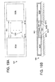
図18A〜図18Dは、例示的なコネクタ・システム763を示しており、これは、集積回路パッケージ761Aと761Bとの間において、または集積回路パッケージ761とプリント回路ボード(メモリ・モジュールのようなモジュールを含む)との間において、ダイレクトコネクト・ケーブル接続を確立するのに使用することができる。先ず、図18Aおよび図18Bにおいては、接続は、“クラム・シェル(clam shell)”状のコネクタ・システム763により行い、これは、伝送ケーブル760を、プレーナのインラインまたはアレイのコンタクトにより、相互接続コンポーネントのエッジに整列させしっかりホールドする(例えば、集積回路パッケージ761の基板またはプリント回路ボードまたはモジュール)。
FIGS. 18A-18D illustrate an
図18Cにより詳細に示した実施形態においては、クラム・シェル接続システム763は、以下のものを含んでいる。すなわち、平らなクラムシェル・コネクタ773の上部リップ(電気的接続を基板の上面においてのみ作るべき用途のため)と、インターコネクト・コンポーネント761の基板の厚さのスペーサ772を含むクラムシェル・コネクタ771の底部リップと、インターコネクト・コンポーネント761上に配置された導体(図18Dに792で示す)との間で電気信号を運び、またケーブル760の導体またはインターコネクト・コンポーネント761の導体のいずれかにある盛り上がり表面または突出構造(すなわち、端子として作用)を通して接続を行うフレックスの回路/伝送ケーブル760と、インターコネクト・コンポーネント761のコンタクト端子に対するダイレクトコネクト・ケーブルの位置合わせを確実に行い、また機械的なアンカーを提供して衝撃または振動により意図しないプルオフを防止する位置合わせピン781と、コネクタ771と773の上部リップと底部リップが、これらがz方向に動くときに互いに位置合わせ状態を保持できるようにするガイド・ピン775(代替の実施形態ではより多いまたはより少ないガイド・ピンを設けることもできる)と、コネクタの各半部を挿入に対してあるいは取り外しが必要なときは取り外しに対して互いに離れる方向に偏倚させるスプリング777と、クラムシェル771,773の上部リップと底部リップを、インターコネクト・コンポーネント761の対応する表面に対し物理的にクランプする締結機構779(例えば、ネジ、または他の閉止力伝達デバイス)とである。ここで、インターコネクト・コンポーネント(例えば、集積回路パッケージ基板、プリント回路ボードまたはモジュール等)は、位置合わせピン781を受けるような形状にした、孔またはスロットのような凹部区域を含んでいる。図18Bおよび図18Cにおいては2つの位置合わせピン781を示しているが、代替の実施形態においては、それより多いまたは少ない位置合わせピン781を設けることもできる。尚、スペーサ772がインターコネクト・コンポーネント761のエッジに当接してインターコネクト・コンポーネント761に向かって延びる方向における位置合わせを制御するように、クラムシェル・コネクタ・システム763を設計する場合、単一の位置合わせ孔を使うこともでき、これによって、インターコネクト・コンポーネント761のエッジに沿った横方向における位置合わせを確立することができる。また、ピンではなく、長手方向の突起(例えば、フィンまたはブレード)あるいは他の突起幾何形状を使用することができ、これにより、コネクタ・システム763とインターコネクト・コンポーネント761の間の位置合わせを確立することができ、そしてインターコネクト・コンポーネント761内の凹部区域785(例えば、孔、チャンネル、溝等)は、その突起幾何形状にしたがった形状とする。位置合わせピン781は、コネクタ・システム763のリップ771および773の一方または両方に配置することもできる。また、これら位置合わせピンは、代替的には、インターコネクト・コンポーネント761上に配置することができ、そして凹部区域785をリップ771および773の一方または両方に配置することもできる。
In the embodiment shown in greater detail in FIG. 18C, clam
続けて図18Cを参照すると、コネクタ・システム763の喉部(すなわち、リップ771および773のインターコネクト・コンポーネント761より上への延長)の深さは、重要ではないが、より薄いスペーサ772が使用される場合、より浅い喉部は剛性を向上させることができる。また、コネクタ771の底部リップは、上部リップ773と同じ深さのものとする必要はなく、したがって1実施形態では、より浅い深さのものとする。上述したように、底部リップ771はまた、より大きな機械的堅牢性のために位置合わせピン781を含むこともできる。また、図18Dに示したように、コネクタの底部リップ771の厚さを、パッケージ基板とプリント回路ボード790との間の予期される隙間794よりも小さな値に減少させる(その隙間は、少なくとも部分的に、パッケージ−ボード間コンタクト791の性質により決まる)。コネクタの上部リップおよび底部リップ771および773は、任意の材料から形成することができ、そして導電性材料で作る場合、これらは、ケーブル760およびインターコネクト・コンポーネント761の一方または双方内のグランド基準(例えば、シールド層)に結合することもできる。1実施形態では、位置合わせピン781を使用することによって、インターコネクト・コンポーネント761上またはインターコネクト・コンポーネント761内に配置されたグランド基準導体(またはグランド・プレーン)および電源電圧導体の一方または双方に係合するようにし、これにより、グランドおよび電源の一方または双方の接続を確立する。
With continued reference to FIG. 18C, the depth of the throat of connector system 763 (ie, the extension of
図18Dを参照すると、ケーブル760上に配置された電気コンタクト・ポイント794(例えば、パッド)とインターコネクト・コンポーネント761上の対応する導体792との間の位置合わせは、位置合わせピン781により確立する。1実施形態においては、インターコネクト・コンポーネント761内の位置合わせ孔785は、基板導体792の端部に対して指定した位置で穿孔する。この位置合わせピンのためのスルーホール796も、ケーブル760において、ケーブル・コンタクト794に対し指定した位置で穿孔する。コネクタ上部リップ773の位置合わせピン781が、ケーブル760のスルーホール796中に挿入されると、このコネクタがインターコネクト・コンポーネント761に閉じられるときに、ケーブル・コンタクト794は、導体792の端部に接触するように位置合わせされる。図18Cに示したように、位置合わせピン781の先端は、ピン781のセルフ・アライメントを可能にするため、先細とすることもできる。
Referring to FIG. 18D, alignment between electrical contact points 794 (eg, pads) disposed on
ダイレクトコネクト・ケーブル導体とインターコネクト・コンポーネント761状のトレース792との間に電気的コンタクトを確立するのに使用する構造は、これに限定する訳ではないが、金ドット、ナノピアス・コンタクト、ポゴピン、エラストマ・パッド、マイクロ・スプリング、メッキ・バンプ、粒子インターコネクト、異方性導電性フィルム等を含むことができる。異なったバンプ・コンタクト間の高さの共面性、特に高いピン・カウントに対するものは、任意の多くの技術を使用して実現することができ、それら技術には、これに限定する訳ではないが、ダイレクトコネクト・ケーブルとコネクタの上部リップとの間のエラストマをサンドイッチすること、および図18Dに示したようなダイレクトコネクト・ケーブル導体上の任意のバンプ・コンタクト794の背後のスプリング装荷コンタクト795の一方または双方が含まれる。
The structure used to establish electrical contact between the direct connect cable conductor and the
図17Eおよび図17Fで上述したように、ダイレクトコネクト・ケーブルは、一端を集積回路パッケージにそして他端をプリント回路ボードまたは回路ボード(またはモジュール)コネクタに結合することができる。したがって、ダイレクトコネクト・ケーブルは、図18A〜図18Dで説明したコネクタ・システム763を、一端にのみ含むことができる。このコネクタの他端は、プリント回路ボード(またはモジュール)への接続のため表面実装タイプまたはメザニン・タイプのコネクタを含むようにしたり、あるいは、例えば図17Fに示したようなボードまたはモジュールのコネクタのコンタクトへの接続に対し適合させるようにしたりできる。
As described above in FIGS. 17E and 17F, the direct connect cable may be coupled at one end to an integrated circuit package and at the other end to a printed circuit board or circuit board (or module) connector. Therefore, the direct connect cable can include the
図19Aおよび図19Bは、本発明の別の実施形態によるダイレクトコネクト信号システムを示している。図19Aは、集積回路パッケージ820の上面図であって、このパッケージは、共用のパッケージ基板上に配置された多数の集積回路ダイ823Aおよび823Bを有している(図19Aには、2つのダイを示しているが、他の実施形態では、任意の数のダイを設けることができる)。このような集積回路パッケージ(これは本文では多チップ・モジュール(MCM)と呼ぶ)においては、それらダイ823間の相互接続は、通常、共用基板821のトレースがプリントされた1つ以上の層により行われる。このアプローチに対する1つの欠点は、一旦基板821に実装すると、個々のダイ823の高速のテストが、1つ以上の他のダイ823への接続により困難となることである。他のダイ823が、ある場合には、高インピーダンスのノード(例えば、3状態にされたすべてのI/O回路)内に置かれることがあるが、このような他のダイ823への基板トレースは、高速シグナリング・テスト中はスタブとして作用する傾向があり、これは、信号品質を劣化させ、ランタイム周波数でのテストを困難にするかもしくは不可能とする。また、個々のダイは、ウエハ・プロービング技術を使ってテストすることもできるが、それらプローブの比較的高いインダクタンスは、通常、ランタイム周波数でのテストを妨げる。その結果、多チップ・モジュールは、完全に組み立てられて、そしてその集積された形態でテストされることが多い。このアプローチでの問題は、多チップ・モジュール内のダイのうちの任意のものが欠陥であった場合、多チップ・モジュール全体が通常廃棄されることである。
19A and 19B illustrate a direct connect signaling system according to another embodiment of the present invention. FIG. 19A is a top view of an
本発明の1実施形態においては、多チップ・モジュールに関連するテスト容易性問題の多くは、ダイレクトコネクト・ケーブルを使用してダイ間に高速リンク(例えば、信号経路)を確立することにより、克服される(あるいは少なくとも軽減される)。したがって、図19Aにおける不連続部825(“x-----x”)により示すように、ダイ間の基板トレース接続は、不完全なままとされ、そして代わりとしてそれらトレースは、ダイレクトコネクト・ケーブル内の電気信号導体と接触するように構成したコンタクト・ゾーン(827A,827B)において終端される。図19Bは、図19Aの配置の側面図であり、ダイレクトコネクト・ケーブル841の配置を示している。ダイレクトコネクト・ケーブル841は、1対のコネクタ843A,843Bを含み、これらは、集積回路ダイ823A,823Bのコンタクトから延在した各組のトレースにより確立されたコンタクト・ゾーン827A,827Bに対し、恒久的にもしくは取り外し可能に固着される。この配置により、各ダイ823がパッケージ基板821に装着されると、高速回路テスタ(図示せず)は、ダイレクトコネクト・テスト・ケーブル(例えば、パッケージ・ダイ823を互いに相互接続するのに使用するケーブル841に対応したケーブル)を使って対応するコンタクト・ゾーン827に結合し、そしてランタイム周波数でテストすることができる。もしこのダイがテストに合格すると、別のダイをパッケージに装着し、そしてこの別のダイを、合格したダイの対またはグループ間にダイレクトコネクト・ケーブル841を結合した状態で、同様にテストする。もし1つのダイが、テストに合格しなかったとすると、これを基板から取り外し、そして別のダイと交換する。あるいは、その部分的に組み立てたモジュールを廃棄することもできる。いずれにしても、個々のダイは、多チップ・モジュール全体の組立を完成させる必要なしで、ランタイム周波数でテストすることができる。尚、図19Aおよび図19Bに示した多チップ・モジュール820はプレーナ・スタイルのモジュール(すなわち、すべてのダイが、同一の平面、例えば、共通基板821の表面に装着されたもの)であるが、ダイレクトコネクト・ケーブルは、スタック形多チップ・モジュールの異なった平面に装着されたダイの間の高速信号経路を形成するのにも使用することができる。
In one embodiment of the present invention, many of the testability problems associated with multichip modules are overcome by establishing high speed links (eg, signal paths) between dies using direct connect cables. (Or at least reduced). Thus, as indicated by the discontinuity 825 (“x ---- x”) in FIG. 19A, the substrate trace connections between the dies remain incomplete, and instead they are connected directly to Terminated in contact zones (827A, 827B) configured to contact electrical signal conductors in the cable. FIG. 19B is a side view of the arrangement of FIG. 19A and shows the arrangement of the
図20は、テスト配置を示しており、これは、ダイレクトコネクト・ケーブルを介して相互接続されるべき回路ボード実装した集積回路パッケージ879A,879Bをテストするのに使うことができる。これと類似の配置を、ダイレクトコネクト・ケーブルを介して相互接続すべき多チップ・モジュールの基板上に装着されたダイをテストするのに使うことができる。点線881は、これから取り付けるべきダイレクトコネクト接続ケーブルの導体の経路を示し、883は、高速テスト装置(例えば、プログラムしたパターンのテスト信号を発生する装置)へのダイレクトコネクト・ケーブル取り付けを示している。集積回路パッケージ879A,879B間の相互接続はまだ確立していないため、パッケージ879Aは、879Bをテストするために高インピーダンス状態に駆動される必要はない。また、プリント回路ボード877上のテスト・ポイントに接触するためにプローブを使用するボード・レベルのテストとは異なり、プリント回路ボード・トレースのスタブ部分からの寄生容量および信号反射は、回避され、これにより高速テスト装置がランタイム周波数でシグナリング・テストを実行できるようにする。パッケージ879Bをテストした後、集積回路パッケージ879Bへのダイレクトコネクト・ケーブル接続を取り外し、そして集積回路パッケージ879Aへのダイレクトコネクト・ケーブル接続を確立する。このように、ボード・レベルの集積回路パッケージ・テストを、ランタイム周波数で、一時に1つの集積回路パッケージにて実行することができる。ダイレクトコネクト・ケーブルは、パッケージ・レベルのテストに合格したと判定した集積回路パッケージの各対(または集積回路パッケージのグループ)間に固着することができる。
FIG. 20 shows a test arrangement, which can be used to test circuit board mounted integrated circuit packages 879A, 879B to be interconnected via direct connect cables. A similar arrangement can be used to test dies mounted on the substrate of a multichip module to be interconnected via direct connect cables.
以上、本発明について特定の例示の実施形態を参照して説明したが、特許請求の範囲に記載した本発明の要旨および範囲から逸脱せずに、種々の修正、変更を行えることが明かである。したがって、本明細書および図面は、限定する意味でなく、例示として見なされるべきである。 Although the present invention has been described with reference to specific exemplary embodiments, it will be apparent that various modifications and changes can be made without departing from the spirit and scope of the invention as set forth in the claims. . The specification and drawings are accordingly to be regarded in an illustrative rather than restrictive sense.
Claims (105)
基板と、
該基板の第1の表面に配置され、第1の複数のコンタクトを含む集積回路ダイと、
前記基板の前記第1表面に配置された複数の導電性トレースであって、前記第1表面に沿って前記第1の複数のコンタクトから前記第1表面の露出領域まで延在した、前記の複数の導電性トレースと、
を備えた集積回路パッケージ。 An integrated circuit package,
A substrate,
An integrated circuit die disposed on the first surface of the substrate and including a first plurality of contacts;
A plurality of conductive traces disposed on the first surface of the substrate, the plurality of conductive traces extending from the first plurality of contacts along the first surface to an exposed region of the first surface; Conductive traces of
Integrated circuit package with
前記基板に固着されたコネクタであって、前記導電性トレースの端子端部に接触する複数の導電性コンタクトを有する、前記のコネクタと、
前記複数の導電性トレースの前記端子端部に対し、前記複数の導電性コンタクトを介して結合された複数の導体を有するケーブルと、
を備えたこと、を特徴とする集積回路パッケージ。 The integrated circuit package of claim 1, further comprising:
A connector affixed to the substrate, the connector having a plurality of conductive contacts in contact with terminal ends of the conductive traces; and
A cable having a plurality of conductors coupled to the terminal ends of the plurality of conductive traces via the plurality of conductive contacts;
An integrated circuit package characterized by comprising:
第1の組のコンタクトと第2の組のコンタクトとを有する集積回路ダイと、
該集積回路ダイに隣接して配置された第1の表面と、該第1表面と対向する第1の表面とを有する基板と、
前記第1組のコンタクトに結合した第1の組の導電性構造であって、前記第1表面から前記基板を貫通して前記第2表面へ延在する、前記の第1組の導電性構造と、
前記第2組のコンタクトに結合した第2の組の導電性構造であって、前記第1表面と第2表面との間に形成された前記基板のエッジまで延在する、前記の第2の組の導電性構造と、
を備えた集積回路パッケージ。 An integrated circuit package,
An integrated circuit die having a first set of contacts and a second set of contacts;
A substrate having a first surface disposed adjacent to the integrated circuit die, and a first surface opposite the first surface;
A first set of conductive structures coupled to the first set of contacts, wherein the first set of conductive structures extends from the first surface through the substrate to the second surface. When,
A second set of conductive structures coupled to the second set of contacts, the second set of conductive structures extending to an edge of the substrate formed between the first surface and the second surface; A set of conductive structures;
Integrated circuit package with
前記第1表面と第2表面との間において前記基板内に配置され、かつ前記基板の前記エッジまで延在する複数の導電性トレースと、
前記複数の導電性トレースと接触するため前記第1表面から延在した複数の導電性ビアと、
を備えたこと、を特徴とする集積回路パッケージ。 30. The integrated circuit package of claim 29, wherein the second set of conductive structures is
A plurality of conductive traces disposed in the substrate between the first surface and the second surface and extending to the edge of the substrate;
A plurality of conductive vias extending from the first surface to contact the plurality of conductive traces;
An integrated circuit package characterized by comprising:
プリント回路ボードと、
該プリント回路ボード上に配置された第1の集積回路パッケージと、
前記プリント回路ボード上に配置された第2の集積回路パッケージと、
前記プリント回路ボード上に浮遊させた複数の電気信号導体であって、前記第1集積回路パッケージと第2集積回路パッケージとの間に延在する、前記の複数の電気信号導体と、
を備えた信号システム。 A signaling system,
A printed circuit board,
A first integrated circuit package disposed on the printed circuit board;
A second integrated circuit package disposed on the printed circuit board;
A plurality of electrical signal conductors suspended on the printed circuit board, the plurality of electrical signal conductors extending between the first integrated circuit package and the second integrated circuit package;
Signal system with
基板と、
該基板の第1の表面に配置され、第1の複数のコンタクトを含む集積回路ダイと、
前記基板の前記第1表面に配置され、かつ前記第1表面に沿って前記第1の複数のコンタクトから前記第1表面の露出領域まで延在した複数の導電性トレースであって、前記第1コネクタが、前記複数の導電性トレースに対し前記露出領域において結合された、前記の複数の導電性トレースと、
を含むこと、を特徴とする信号システム。 49. The signaling system of claim 48, wherein the first integrated circuit package is
A substrate,
An integrated circuit die disposed on the first surface of the substrate and including a first plurality of contacts;
A plurality of conductive traces disposed on the first surface of the substrate and extending along the first surface from the first plurality of contacts to an exposed region of the first surface; The plurality of conductive traces, wherein a connector is coupled to the plurality of conductive traces in the exposed region;
Including a signal system.
前記プリント回路ボードに装着された第3の集積回路パッケージと、
前記プリント回路ボード上に浮遊させ、かつ前記第1集積回路パッケージと第3集積回路パッケージとの間に延在した第2の複数の電気信号導体と、
を含むこと、を特徴とする信号システム。 40. The signal system of claim 39, wherein the plurality of electrical signal conductors extending between the first integrated circuit package and the second integrated circuit package constitute a first plurality of electrical signal conductors, The system further
A third integrated circuit package mounted on the printed circuit board;
A second plurality of electrical signal conductors suspended on the printed circuit board and extending between the first and third integrated circuit packages;
Including a signal system.
前記第1の複数の電気信号導体の第1の端部に固着され、かつ前記第1集積回路パッケージに結合された第1のコネクタと、
前記第2の複数の電気信号導体の第1の端部に固着され、かつ前記第1集積回路パッケージに結合された第2のコネクタと、
を含むこと、を特徴とする信号システム。 53. A signaling system according to claim 52, further comprising:
A first connector secured to a first end of the first plurality of electrical signal conductors and coupled to the first integrated circuit package;
A second connector secured to a first end of the second plurality of electrical signal conductors and coupled to the first integrated circuit package;
Including a signal system.
プリント回路ボードと、
該プリント回路ボード上に配置された第1の集積回路パッケージと、
前記プリント回路ボード上に配置された第2の集積回路パッケージと、
前記第1集積回路パッケージと前記第2集積回路パッケージとに固着されたケーブルであって、複数の電気信号導体を含む、前記のケーブルと、
を備えた信号システム。 A signaling system,
A printed circuit board,
A first integrated circuit package disposed on the printed circuit board;
A second integrated circuit package disposed on the printed circuit board;
A cable secured to the first integrated circuit package and the second integrated circuit package, the cable including a plurality of electrical signal conductors;
Signal system with
第1の回路ボードと、
該第1回路ボード上に配置され、かつ第1のインバータ上に配置された第1の集積回路ダイを含む第1の集積回路パッケージと、
第2の基板上に配置された第2の集積回路ダイを含む第2の集積回路パッケージと、
前記第1基板と前記第2基板とに固着された、複数の電気信号導体を含むケーブルと、
を備えた信号システム。 A signaling system,
A first circuit board;
A first integrated circuit package including a first integrated circuit die disposed on the first circuit board and disposed on a first inverter;
A second integrated circuit package including a second integrated circuit die disposed on a second substrate;
A cable including a plurality of electrical signal conductors secured to the first substrate and the second substrate;
Signal system with
基板と、
該基板上に配置された第1の集積回路ダイと、
該基板上に配置された第2の集積回路ダイと、
前記第1集積回路ダイと第2集積回路ダイとの間に電気的に結合されたケーブルと、
を備えた集積回路パッケージ。 An integrated circuit package for mounting on a circuit board,
A substrate,
A first integrated circuit die disposed on the substrate;
A second integrated circuit die disposed on the substrate;
A cable electrically coupled between the first integrated circuit die and the second integrated circuit die;
Integrated circuit package with
前記第1ダイを、前記集積回路パッケージの表面に装着し、
前記第1ダイを前記基板に装着した後に、前記第1ダイをテスト装置でテストし、
前記第2ダイを前記基板に装着し、
前記第2ダイを前記基板に装着した後に、前記第2ダイを前記テスト装置でテストし、
前記テスト装置により前記第1ダイと前記第2ダイを成功裏にテストできた場合、前記第1ダイと前記第2ダイとの間に第1のケーブルを結合すること、
を備えた製造方法。 A method for manufacturing an integrated circuit package comprising a first die and a second die, comprising:
Mounting the first die on the surface of the integrated circuit package;
After mounting the first die on the substrate, the first die is tested with a test device;
Attaching the second die to the substrate;
After mounting the second die on the substrate, testing the second die with the test device;
If the test device has successfully tested the first die and the second die, coupling a first cable between the first die and the second die;
A manufacturing method comprising:
前記基板上に配置されかつ前記第1ダイのコンタクトに接続された第1の複数のトレースに対し、前記第1ケーブルの第1の端部を結合し、
前記基板上に配置されかつ前記第2ダイのコンタクトに接続された第2の複数のトレースに対し、前記第1ケーブルの第2の端部を結合すること、
を含むこと、を特徴とする製造方法。 94. The method of claim 93, wherein the first cable is coupled between the first die and the second die.
Coupling a first end of the first cable to a first plurality of traces disposed on the substrate and connected to contacts of the first die;
Coupling a second end of the first cable to a second plurality of traces disposed on the substrate and connected to contacts of the second die;
The manufacturing method characterized by including.
Applications Claiming Priority (3)
| Application Number | Priority Date | Filing Date | Title |
|---|---|---|---|
| US37648202P | 2002-04-29 | 2002-04-29 | |
| US40018002P | 2002-07-31 | 2002-07-31 | |
| PCT/US2003/013524 WO2003094203A2 (en) | 2002-04-29 | 2003-04-29 | Direct-connect signaling system |
Related Child Applications (1)
| Application Number | Title | Priority Date | Filing Date |
|---|---|---|---|
| JP2010089212A Division JP5437137B2 (en) | 2002-04-29 | 2010-04-08 | Direct connect signal system |
Publications (2)
| Publication Number | Publication Date |
|---|---|
| JP2005524239A true JP2005524239A (en) | 2005-08-11 |
| JP2005524239A5 JP2005524239A5 (en) | 2006-06-15 |
Family
ID=29406757
Family Applications (2)
| Application Number | Title | Priority Date | Filing Date |
|---|---|---|---|
| JP2004502330A Withdrawn JP2005524239A (en) | 2002-04-29 | 2003-04-29 | Direct connect signal system |
| JP2010089212A Expired - Fee Related JP5437137B2 (en) | 2002-04-29 | 2010-04-08 | Direct connect signal system |
Family Applications After (1)
| Application Number | Title | Priority Date | Filing Date |
|---|---|---|---|
| JP2010089212A Expired - Fee Related JP5437137B2 (en) | 2002-04-29 | 2010-04-08 | Direct connect signal system |
Country Status (6)
| Country | Link |
|---|---|
| US (2) | US7307293B2 (en) |
| EP (1) | EP1506568B1 (en) |
| JP (2) | JP2005524239A (en) |
| CN (1) | CN1659810B (en) |
| AU (1) | AU2003223783A1 (en) |
| WO (1) | WO2003094203A2 (en) |
Cited By (6)
| Publication number | Priority date | Publication date | Assignee | Title |
|---|---|---|---|---|
| JP2011515762A (en) * | 2008-03-21 | 2011-05-19 | ソニー株式会社 | Innovative method to build a bus-based switching scheme for HDMI or similar I / F |
| JP2012503887A (en) * | 2008-09-29 | 2012-02-09 | インテル コーポレイション | Mounted processor I / O architecture |
| WO2018124004A1 (en) * | 2016-12-28 | 2018-07-05 | 株式会社村田製作所 | Electronic device |
| WO2018142884A1 (en) * | 2017-02-03 | 2018-08-09 | 株式会社村田製作所 | Interposer and electronic device |
| KR20190044622A (en) * | 2016-09-19 | 2019-04-30 | 인텔 코포레이션 | Alternative circuit devices for long host routing |
| JP2022511581A (en) * | 2019-11-15 | 2022-02-01 | バイドゥ ドットコム タイムス テクノロジー (ベイジン) カンパニー リミテッド | Distributed AI training topology based on flexible cable connections |
Families Citing this family (131)
| Publication number | Priority date | Publication date | Assignee | Title |
|---|---|---|---|---|
| US7750446B2 (en) * | 2002-04-29 | 2010-07-06 | Interconnect Portfolio Llc | IC package structures having separate circuit interconnection structures and assemblies constructed thereof |
| US7307293B2 (en) * | 2002-04-29 | 2007-12-11 | Silicon Pipe, Inc. | Direct-connect integrated circuit signaling system for bypassing intra-substrate printed circuit signal paths |
| US6897556B2 (en) * | 2003-09-08 | 2005-05-24 | Intel Corporation | I/O architecture for integrated circuit package |
| US7345359B2 (en) * | 2004-03-05 | 2008-03-18 | Intel Corporation | Integrated circuit package with chip-side signal connections |
| KR100632469B1 (en) * | 2004-04-20 | 2006-10-09 | 삼성전자주식회사 | Semiconductor chip package |
| US8217381B2 (en) * | 2004-06-04 | 2012-07-10 | The Board Of Trustees Of The University Of Illinois | Controlled buckling structures in semiconductor interconnects and nanomembranes for stretchable electronics |
| EP2650906A3 (en) | 2004-06-04 | 2015-02-18 | The Board of Trustees of the University of Illinois | Methods and devices for fabricating and assembling printable semiconductor elements |
| US7521292B2 (en) | 2004-06-04 | 2009-04-21 | The Board Of Trustees Of The University Of Illinois | Stretchable form of single crystal silicon for high performance electronics on rubber substrates |
| US7262121B2 (en) * | 2004-07-29 | 2007-08-28 | Micron Technology, Inc. | Integrated circuit and methods of redistributing bondpad locations |
| US7705445B2 (en) * | 2005-02-11 | 2010-04-27 | Rambus Inc. | Semiconductor package with low and high-speed signal paths |
| JP4470784B2 (en) * | 2005-03-28 | 2010-06-02 | トヨタ自動車株式会社 | Semiconductor device |
| TWI533459B (en) * | 2005-06-02 | 2016-05-11 | 美國伊利諾大學理事會 | Printable semiconductor structures and related methods of making and assembling |
| US20060289981A1 (en) * | 2005-06-28 | 2006-12-28 | Nickerson Robert M | Packaging logic and memory integrated circuits |
| US7518238B2 (en) * | 2005-12-02 | 2009-04-14 | Intel Corporation | Mounting flexible circuits onto integrated circuit substrates |
| US8102184B2 (en) | 2006-01-17 | 2012-01-24 | Johnstech International | Test contact system for testing integrated circuits with packages having an array of signal and power contacts |
| US7569916B2 (en) * | 2006-03-14 | 2009-08-04 | Paricon Technologies Corp. | Separable network interconnect systems and assemblies |
| US7746661B2 (en) * | 2006-06-08 | 2010-06-29 | Sandisk Corporation | Printed circuit board with coextensive electrical connectors and contact pad areas |
| TWI351085B (en) * | 2006-08-08 | 2011-10-21 | Silicon Base Dev Inc | Structure and manufacturing method of package base for power semiconductor device |
| US20080157320A1 (en) * | 2006-12-29 | 2008-07-03 | Harrison Ray D | Laterally Interconnected IC Packages and Methods |
| WO2008090558A2 (en) * | 2007-01-24 | 2008-07-31 | Gidel Ltd. | Device, system, and method of flexible hardware connectivity |
| US7978030B2 (en) * | 2007-02-12 | 2011-07-12 | Finisar Corporation | High-speed interconnects |
| US7859367B2 (en) * | 2007-02-12 | 2010-12-28 | Finisar Corporation | Non-coplanar high-speed interconnects |
| US20080229371A1 (en) * | 2007-02-22 | 2008-09-18 | Mick Colin K | Digital multimedia network including method and apparatus for high speed user download of digital files |
| US20080228964A1 (en) * | 2007-03-13 | 2008-09-18 | Henning Braunisch | Hybrid flex-and-board memory interconnect system |
| KR101150454B1 (en) * | 2007-08-06 | 2012-06-01 | 삼성전자주식회사 | Memory module having star-type topology and method of fabricating the same |
| DE102007044602A1 (en) * | 2007-09-19 | 2009-04-23 | Continental Automotive Gmbh | Multilayer printed circuit board and use of a multilayer printed circuit board |
| US7880570B2 (en) * | 2007-10-25 | 2011-02-01 | Finisar Corporation | Feed thru with flipped signal plane using guided vias |
| US7671450B2 (en) * | 2007-12-17 | 2010-03-02 | Agere Systems Inc. | Integrated circuit package for high-speed signals |
| JP5743553B2 (en) * | 2008-03-05 | 2015-07-01 | ザ ボード オブ トラスティーズ オブ ザ ユニヴァーシティー オブ イリノイ | Stretchable and foldable electronic devices |
| US7888784B2 (en) * | 2008-09-30 | 2011-02-15 | Intel Corporation | Substrate package with through holes for high speed I/O flex cable |
| US8886334B2 (en) | 2008-10-07 | 2014-11-11 | Mc10, Inc. | Systems, methods, and devices using stretchable or flexible electronics for medical applications |
| US8389862B2 (en) | 2008-10-07 | 2013-03-05 | Mc10, Inc. | Extremely stretchable electronics |
| EP2349440B1 (en) | 2008-10-07 | 2019-08-21 | Mc10, Inc. | Catheter balloon having stretchable integrated circuitry and sensor array |
| US8372726B2 (en) | 2008-10-07 | 2013-02-12 | Mc10, Inc. | Methods and applications of non-planar imaging arrays |
| US8097926B2 (en) | 2008-10-07 | 2012-01-17 | Mc10, Inc. | Systems, methods, and devices having stretchable integrated circuitry for sensing and delivering therapy |
| US9011177B2 (en) | 2009-01-30 | 2015-04-21 | Molex Incorporated | High speed bypass cable assembly |
| TWI592996B (en) | 2009-05-12 | 2017-07-21 | 美國伊利諾大學理事會 | Printed assemblies of ultrathin, microscale inorganic light emitting diodes for deformable and semitransparent displays |
| US8339760B2 (en) * | 2009-06-15 | 2012-12-25 | Apple Inc. | Thermal protection circuits and structures for electronic devices and cables |
| US9322542B2 (en) | 2009-08-12 | 2016-04-26 | Edward Bryant Stoneham | Versatile sealed LED lamp |
| WO2011041727A1 (en) | 2009-10-01 | 2011-04-07 | Mc10, Inc. | Protective cases with integrated electronics |
| US8498087B2 (en) * | 2009-11-03 | 2013-07-30 | Apple Inc. | Thermal protection circuits for electronic device cables |
| US9936574B2 (en) | 2009-12-16 | 2018-04-03 | The Board Of Trustees Of The University Of Illinois | Waterproof stretchable optoelectronics |
| WO2011084450A1 (en) | 2009-12-16 | 2011-07-14 | The Board Of Trustees Of The University Of Illinois | Electrophysiology in-vivo using conformal electronics |
| US10441185B2 (en) | 2009-12-16 | 2019-10-15 | The Board Of Trustees Of The University Of Illinois | Flexible and stretchable electronic systems for epidermal electronics |
| KR101729507B1 (en) * | 2010-06-30 | 2017-04-24 | 삼성전자 주식회사 | Printed circuit board unit and computer device having the same |
| JP2012064338A (en) * | 2010-09-14 | 2012-03-29 | Fujitsu Ltd | Terminal structure of coaxial cable, connector and board unit |
| KR101871865B1 (en) | 2010-09-18 | 2018-08-02 | 페어차일드 세미컨덕터 코포레이션 | Multi-die mems package |
| KR20130052652A (en) | 2010-09-18 | 2013-05-22 | 페어차일드 세미컨덕터 코포레이션 | Sealed packaging for microelectromechanical systems |
| WO2012037538A2 (en) | 2010-09-18 | 2012-03-22 | Fairchild Semiconductor Corporation | Micromachined monolithic 6-axis inertial sensor |
| WO2012037501A2 (en) | 2010-09-18 | 2012-03-22 | Cenk Acar | Flexure bearing to reduce quadrature for resonating micromachined devices |
| US9278845B2 (en) | 2010-09-18 | 2016-03-08 | Fairchild Semiconductor Corporation | MEMS multi-axis gyroscope Z-axis electrode structure |
| EP2616772B1 (en) | 2010-09-18 | 2016-06-22 | Fairchild Semiconductor Corporation | Micromachined monolithic 3-axis gyroscope with single drive |
| CN103221795B (en) | 2010-09-20 | 2015-03-11 | 快捷半导体公司 | Microelectromechanical pressure sensor including reference capacitor |
| US8841560B1 (en) * | 2010-11-17 | 2014-09-23 | Dawn VME Products | Backplane slot interconnection system, method and apparatus |
| CA2829986C (en) * | 2011-03-21 | 2015-02-10 | University Of Windsor | Apparatus for the automated testing and validation of electronic components |
| WO2012138924A1 (en) * | 2011-04-06 | 2012-10-11 | Huawei Technologies Co., Ltd. | Method for expanding a single chassis network or computing platform using soft interconnects |
| CN103609037A (en) * | 2011-04-06 | 2014-02-26 | 华为技术有限公司 | Method for expanding a single chassis network or computing platform using soft interconnects |
| WO2012158709A1 (en) | 2011-05-16 | 2012-11-22 | The Board Of Trustees Of The University Of Illinois | Thermally managed led arrays assembled by printing |
| JP2014523633A (en) | 2011-05-27 | 2014-09-11 | エムシー10 インコーポレイテッド | Electronic, optical and / or mechanical devices and systems and methods of manufacturing these devices and systems |
| US8934965B2 (en) | 2011-06-03 | 2015-01-13 | The Board Of Trustees Of The University Of Illinois | Conformable actively multiplexed high-density surface electrode array for brain interfacing |
| US9324678B2 (en) | 2011-12-20 | 2016-04-26 | Intel Corporation | Low profile zero/low insertion force package top side flex cable connector architecture |
| JP5795541B2 (en) * | 2012-01-05 | 2015-10-14 | 株式会社東海理化電機製作所 | Detection signal output device |
| US9062972B2 (en) | 2012-01-31 | 2015-06-23 | Fairchild Semiconductor Corporation | MEMS multi-axis accelerometer electrode structure |
| JP2015521303A (en) | 2012-03-30 | 2015-07-27 | ザ ボード オブ トラスティーズ オブ ザ ユニヴァーシ | An electronic device that can be attached to the surface and can be attached to an accessory |
| US9488693B2 (en) | 2012-04-04 | 2016-11-08 | Fairchild Semiconductor Corporation | Self test of MEMS accelerometer with ASICS integrated capacitors |
| KR102058489B1 (en) | 2012-04-05 | 2019-12-23 | 페어차일드 세미컨덕터 코포레이션 | Mems device front-end charge amplifier |
| EP2647952B1 (en) | 2012-04-05 | 2017-11-15 | Fairchild Semiconductor Corporation | Mems device automatic-gain control loop for mechanical amplitude drive |
| EP2647955B8 (en) | 2012-04-05 | 2018-12-19 | Fairchild Semiconductor Corporation | MEMS device quadrature phase shift cancellation |
| US9625272B2 (en) | 2012-04-12 | 2017-04-18 | Fairchild Semiconductor Corporation | MEMS quadrature cancellation and signal demodulation |
| US8841845B2 (en) * | 2012-07-24 | 2014-09-23 | Ricardo Montemayor | Proximity-based wireless lighting system |
| US20140027157A1 (en) * | 2012-07-26 | 2014-01-30 | Futurewei Technologies, Inc. | Device and Method for Printed Circuit Board with Embedded Cable |
| CN104704682B (en) | 2012-08-22 | 2017-03-22 | 安费诺有限公司 | High-frequency electrical connector |
| DE102013014881B4 (en) | 2012-09-12 | 2023-05-04 | Fairchild Semiconductor Corporation | Enhanced silicon via with multi-material fill |
| US9171794B2 (en) | 2012-10-09 | 2015-10-27 | Mc10, Inc. | Embedding thin chips in polymer |
| JP2014096667A (en) * | 2012-11-08 | 2014-05-22 | Murata Mfg Co Ltd | Module |
| US9470858B2 (en) | 2013-01-11 | 2016-10-18 | Multiphoton Optics Gmbh | Optical package and a process for its preparation |
| TWI518868B (en) | 2013-02-05 | 2016-01-21 | 聯詠科技股份有限公司 | Integrated circuit |
| CN103996677B (en) * | 2013-02-19 | 2016-12-28 | 联咏科技股份有限公司 | Integrated circuit |
| US9142921B2 (en) | 2013-02-27 | 2015-09-22 | Molex Incorporated | High speed bypass cable for use with backplanes |
| JP6208878B2 (en) | 2013-09-04 | 2017-10-04 | モレックス エルエルシー | Connector system with cable bypass |
| US9837191B2 (en) * | 2014-01-02 | 2017-12-05 | Raytheon Company | Method of connecting an additive communication cable to an electrical harness |
| JP6442713B2 (en) | 2014-03-26 | 2018-12-26 | パナソニックIpマネジメント株式会社 | Electronic device and display device |
| US10451652B2 (en) * | 2014-07-16 | 2019-10-22 | Teradyne, Inc. | Coaxial structure for transmission of signals in test equipment |
| US10297572B2 (en) * | 2014-10-06 | 2019-05-21 | Mc10, Inc. | Discrete flexible interconnects for modules of integrated circuits |
| US9685736B2 (en) | 2014-11-12 | 2017-06-20 | Amphenol Corporation | Very high speed, high density electrical interconnection system with impedance control in mating region |
| CN107112666B (en) | 2015-01-11 | 2019-04-23 | 莫列斯有限公司 | Plate connector assembly, connector and bypass cable-assembly |
| US10135211B2 (en) | 2015-01-11 | 2018-11-20 | Molex, Llc | Circuit board bypass assemblies and components therefor |
| JP6574266B2 (en) | 2015-05-04 | 2019-09-11 | モレックス エルエルシー | Computer device using bypass assembly |
| CN107851208B (en) | 2015-06-01 | 2021-09-10 | 伊利诺伊大学评议会 | Miniaturized electronic system with wireless power supply and near field communication capability |
| EP3304130B1 (en) | 2015-06-01 | 2021-10-06 | The Board of Trustees of the University of Illinois | Alternative approach to uv sensing |
| US20230130045A1 (en) * | 2021-10-27 | 2023-04-27 | Teramount Ltd. | Detachable connector for co-packaged optics |
| KR102497583B1 (en) * | 2015-10-27 | 2023-02-10 | 삼성전자주식회사 | Semiconductor devices having flexible interconnection and methods for fabricating the same |
| US10312967B2 (en) * | 2015-12-15 | 2019-06-04 | Nvidia Corporation | System and method for cross-talk cancellation in single-ended signaling |
| WO2017123574A1 (en) | 2016-01-11 | 2017-07-20 | Molex, Llc | Routing assembly and system using same |
| US10424878B2 (en) | 2016-01-11 | 2019-09-24 | Molex, Llc | Cable connector assembly |
| CN108475870B (en) * | 2016-01-19 | 2019-10-18 | 莫列斯有限公司 | Integrated routing component and the system for using integrated routing component |
| WO2017210276A1 (en) | 2016-05-31 | 2017-12-07 | Amphenol Corporation | High performance cable termination |
| CN110088985B (en) | 2016-10-19 | 2022-07-05 | 安费诺有限公司 | Flexible shield for ultra-high speed high density electrical interconnects |
| US10044155B1 (en) * | 2017-05-10 | 2018-08-07 | Qualcomm Incorporated | Connector for connecting a device to a plurality of pads arranged at different radial distances from the source |
| TW202315246A (en) | 2017-08-03 | 2023-04-01 | 美商安芬諾股份有限公司 | Cable assembly and method of manufacturing the same |
| US20190051587A1 (en) * | 2017-08-11 | 2019-02-14 | Marvell Israel (M.I.S.L) Ltd. | Ic package |
| FR3070573A1 (en) * | 2017-08-25 | 2019-03-01 | Stmicroelectronics (Grenoble 2) Sas | ELECTRONIC DEVICE INCLUDING AT LEAST ONE ELECTRONIC CHIP AND ELECTRONIC ASSEMBLY |
| US10741951B2 (en) | 2017-11-13 | 2020-08-11 | Te Connectivity Corporation | Socket connector assembly for an electronic package |
| US11508663B2 (en) | 2018-02-02 | 2022-11-22 | Marvell Israel (M.I.S.L) Ltd. | PCB module on package |
| US10665973B2 (en) | 2018-03-22 | 2020-05-26 | Amphenol Corporation | High density electrical connector |
| WO2019195319A1 (en) | 2018-04-02 | 2019-10-10 | Ardent Concepts, Inc. | Controlled-impedance compliant cable termination |
| CN109193200B (en) * | 2018-06-08 | 2024-01-23 | 安费诺电子装配(厦门)有限公司 | Wire end connector with rotary lock rod, connector assembly and use method of connector assembly |
| US10716213B2 (en) | 2018-07-28 | 2020-07-14 | Hewlett Packard Enterprise Development Lp | Direct connection of high speed signals on PCB chip |
| CN209016312U (en) | 2018-07-31 | 2019-06-21 | 安费诺电子装配(厦门)有限公司 | A kind of line-end connector and connector assembly |
| US10931062B2 (en) | 2018-11-21 | 2021-02-23 | Amphenol Corporation | High-frequency electrical connector |
| CN111367727B (en) * | 2018-12-25 | 2023-11-17 | 中兴通讯股份有限公司 | Connector structure, and method and device for calculating time delay difference |
| CN113557459B (en) | 2019-01-25 | 2023-10-20 | 富加宜(美国)有限责任公司 | I/O connector configured for cable connection to midplane |
| CN113474706B (en) | 2019-01-25 | 2023-08-29 | 富加宜(美国)有限责任公司 | I/O connector configured for cable connection to midplane |
| CN113728521A (en) | 2019-02-22 | 2021-11-30 | 安费诺有限公司 | High performance cable connector assembly |
| WO2020172743A1 (en) * | 2019-02-25 | 2020-09-03 | Reflex Photonics Inc. | Method and assembly for board to board connection of active devices |
| CN109856499A (en) * | 2019-03-22 | 2019-06-07 | 京东方科技集团股份有限公司 | A kind of driving part and its detection method, display device |
| WO2020250162A1 (en) | 2019-06-10 | 2020-12-17 | Marvell Israel (M.I.S.L) Ltd. | Ic package with top-side memory module |
| US11552432B2 (en) * | 2019-08-12 | 2023-01-10 | High Speed Interconnects, Llc | Methods and apparatus for RF shield and cable attachment system |
| US20190387634A1 (en) * | 2019-08-29 | 2019-12-19 | Intel Corporation | System, apparatus and method for providing a symmetric multi-processor high-speed link |
| WO2021055584A1 (en) | 2019-09-19 | 2021-03-25 | Amphenol Corporation | High speed electronic system with midboard cable connector |
| US11282806B2 (en) | 2019-10-11 | 2022-03-22 | Marvell Asia Pte, Ltd. | Partitioned substrates with interconnect bridge |
| TW202135385A (en) | 2020-01-27 | 2021-09-16 | 美商Fci美國有限責任公司 | High speed connector |
| TW202147716A (en) | 2020-01-27 | 2021-12-16 | 美商Fci美國有限責任公司 | High speed, high density direct mate orthogonal connector |
| CN113258325A (en) | 2020-01-28 | 2021-08-13 | 富加宜(美国)有限责任公司 | High-frequency middle plate connector |
| US11862901B2 (en) | 2020-12-15 | 2024-01-02 | Teradyne, Inc. | Interposer |
| US11604219B2 (en) | 2020-12-15 | 2023-03-14 | Teradyne, Inc. | Automatic test equipement having fiber optic connections to remote servers |
| EP4318564A1 (en) * | 2021-04-29 | 2024-02-07 | Huawei Technologies Co., Ltd. | Circuit board assembly part and electronic device |
| CN115426541A (en) * | 2021-05-17 | 2022-12-02 | 华为技术有限公司 | Electronic component, switch and computer system |
| USD1002553S1 (en) | 2021-11-03 | 2023-10-24 | Amphenol Corporation | Gasket for connector |
| US20230163113A1 (en) * | 2021-11-22 | 2023-05-25 | Qualcomm Incorporated | Package comprising channel interconnects located between solder interconnects |
| US20230299035A1 (en) * | 2022-03-18 | 2023-09-21 | Meta Platforms, Inc. | Flex bonded integrated circuits |
Family Cites Families (135)
| Publication number | Priority date | Publication date | Assignee | Title |
|---|---|---|---|---|
| US3795845A (en) | 1972-12-26 | 1974-03-05 | Ibm | Semiconductor chip having connecting pads arranged in a non-orthogonal array |
| JPS5278069A (en) | 1975-12-24 | 1977-07-01 | Fuji Kinzoku Kakou Kk | Printed circuit board |
| US4095866A (en) | 1977-05-19 | 1978-06-20 | Ncr Corporation | High density printed circuit board and edge connector assembly |
| US4202007A (en) | 1978-06-23 | 1980-05-06 | International Business Machines Corporation | Multi-layer dielectric planar structure having an internal conductor pattern characterized with opposite terminations disposed at a common edge surface of the layers |
| DE3038665C2 (en) | 1980-10-13 | 1990-03-29 | Riba-Prüftechnik GmbH, 7801 Schallstadt | Testing device for testing printed circuit boards provided with conductor tracks |
| FR2495846A1 (en) | 1980-12-05 | 1982-06-11 | Cii Honeywell Bull | ELECTRICAL CONNECTION DEVICE HAVING HIGH DENSITY OF CONTACTS |
| US4458297A (en) | 1981-01-16 | 1984-07-03 | Mosaic Systems, Inc. | Universal interconnection substrate |
| JPS59155950A (en) | 1983-02-25 | 1984-09-05 | Shinko Electric Ind Co Ltd | Low melting-point glass seal type ceramic package for semiconductor device |
| US4543715A (en) | 1983-02-28 | 1985-10-01 | Allied Corporation | Method of forming vertical traces on printed circuit board |
| US4543713A (en) * | 1983-08-08 | 1985-10-01 | At&T Technologies, Inc. | Technique for inserting connector leads into a circuit board |
| US4812792A (en) | 1983-12-22 | 1989-03-14 | Trw Inc. | High-frequency multilayer printed circuit board |
| GB2161033B (en) | 1984-06-21 | 1988-05-25 | Gen Electric Co Plc | Programmable bed-of-nails test access jigs with electro-rheological fluid actuation |
| CA1237820A (en) | 1985-03-20 | 1988-06-07 | Hitachi, Ltd. | Multilayer printed circuit board |
| JPS61287253A (en) * | 1985-06-14 | 1986-12-17 | Hitachi Ltd | Semiconductor device |
| US4644092A (en) * | 1985-07-18 | 1987-02-17 | Amp Incorporated | Shielded flexible cable |
| US4748495A (en) | 1985-08-08 | 1988-05-31 | Dypax Systems Corporation | High density multi-chip interconnection and cooling package |
| US4731643A (en) | 1985-10-21 | 1988-03-15 | International Business Machines Corporation | Logic-circuit layout for large-scale integrated circuits |
| JPS62136098A (en) | 1985-12-09 | 1987-06-19 | 富士通株式会社 | High density wiring board |
| US4881905A (en) | 1986-05-23 | 1989-11-21 | Amp Incorporated | High density controlled impedance connector |
| US4768154A (en) | 1987-05-08 | 1988-08-30 | Telesis Systems Corporation | Computer aided printed circuit board wiring |
| FR2616503B1 (en) * | 1987-06-11 | 1992-07-10 | Ferco Int Usine Ferrures | DOUBLE ACTION SHOCK ABSORBER CAUSING LAMINATION OF A FLUID ON THE PASSAGE OF A THREAD |
| US5136123A (en) | 1987-07-17 | 1992-08-04 | Junkosha Co., Ltd. | Multilayer circuit board |
| US4814945A (en) | 1987-09-18 | 1989-03-21 | Trw Inc. | Multilayer printed circuit board for ceramic chip carriers |
| FR2621173B1 (en) | 1987-09-29 | 1989-12-08 | Bull Sa | HIGH DENSITY INTEGRATED CIRCUIT BOX |
| US4799617A (en) | 1987-10-09 | 1989-01-24 | Advanced Techniques Co., Inc. | Convection heat attachment and removal instrument for surface mounted assemblies |
| US4956749A (en) | 1987-11-20 | 1990-09-11 | Hewlett-Packard Company | Interconnect structure for integrated circuits |
| US4861251A (en) | 1988-02-29 | 1989-08-29 | Diehard Engineering, Inc. | Apparatus for encapsulating selected portions of a printed circuit board |
| US4838800A (en) | 1988-05-23 | 1989-06-13 | Gte Products Corporation | High density interconnect system |
| US4935584A (en) | 1988-05-24 | 1990-06-19 | Tektronix, Inc. | Method of fabricating a printed circuit board and the PCB produced |
| US5019946A (en) | 1988-09-27 | 1991-05-28 | General Electric Company | High density interconnect with high volumetric efficiency |
| US4994938A (en) | 1988-12-28 | 1991-02-19 | Texas Instruments Incorporated | Mounting of high density components on substrate |
| US4991115A (en) | 1989-05-16 | 1991-02-05 | Excellon Industries, Inc. | Method of mapping geometric entities from a continuous plane to a discrete plane |
| JPH07111971B2 (en) | 1989-10-11 | 1995-11-29 | 三菱電機株式会社 | Method of manufacturing integrated circuit device |
| US4960386A (en) | 1989-10-17 | 1990-10-02 | Molex Incorporated | High deflection, high density single sided electrical connector |
| US5185502A (en) | 1989-12-01 | 1993-02-09 | Cray Research, Inc. | High power, high density interconnect apparatus for integrated circuits |
| US4969826A (en) | 1989-12-06 | 1990-11-13 | Amp Incorporated | High density connector for an IC chip carrier |
| US5012924A (en) | 1990-03-19 | 1991-05-07 | R. H. Murphy Company, Inc. | Carriers for integrated circuits and the like |
| US5009611A (en) | 1990-05-23 | 1991-04-23 | Molex Incorporated | High density electrical connector for printed circuit boards |
| US5162792A (en) | 1990-08-03 | 1992-11-10 | American Telephone And Telegraph Company | On-the-fly arrangement for interconnecting leads and connectors |
| US5135123A (en) * | 1990-09-20 | 1992-08-04 | Phoenix Closures, Inc. | Tamper-evident closure with a separately formed break away band |
| US5220490A (en) | 1990-10-25 | 1993-06-15 | Microelectronics And Computer Technology Corporation | Substrate interconnect allowing personalization using spot surface links |
| US5155577A (en) | 1991-01-07 | 1992-10-13 | International Business Machines Corporation | Integrated circuit carriers and a method for making engineering changes in said carriers |
| US5634093A (en) | 1991-01-30 | 1997-05-27 | Kabushiki Kaisha Toshiba | Method and CAD system for designing wiring patterns using predetermined rules |
| US5227013A (en) | 1991-07-25 | 1993-07-13 | Microelectronics And Computer Technology Corporation | Forming via holes in a multilevel substrate in a single step |
| US5165984A (en) | 1991-07-30 | 1992-11-24 | At&T Bell Laboratories | Stepped multilayer interconnection apparatus and method of making the same |
| JPH0536857A (en) * | 1991-07-30 | 1993-02-12 | Toshiba Corp | Semiconductor integrated circuit mounting board |
| US5291375A (en) | 1991-09-30 | 1994-03-01 | Kabushiki Kaisha Toshiba | Printed circuit board and electric device configured to facilitate bonding |
| US5309324A (en) | 1991-11-26 | 1994-05-03 | Herandez Jorge M | Device for interconnecting integrated circuit packages to circuit boards |
| JPH0730224A (en) * | 1991-12-02 | 1995-01-31 | Nippon Telegr & Teleph Corp <Ntt> | Mounting structure for electronic device |
| US5222014A (en) | 1992-03-02 | 1993-06-22 | Motorola, Inc. | Three-dimensional multi-chip pad array carrier |
| US5404047A (en) | 1992-07-17 | 1995-04-04 | Lsi Logic Corporation | Semiconductor die having a high density array of composite bond pads |
| US5417577A (en) | 1992-09-23 | 1995-05-23 | At&T Corp. | Interconnection method and apparatus |
| JP2595541Y2 (en) | 1993-01-13 | 1999-05-31 | 住友電装株式会社 | connector |
| US5306162A (en) * | 1993-04-14 | 1994-04-26 | Compaq Computer Corporation | Clamp connector apparatus for removably coupling a flexible ribbon cable to a printed circuit board |
| DE4313251C2 (en) | 1993-04-23 | 2003-03-27 | Bosch Gmbh Robert | Sensor element for determining the gas component concentration |
| US5572040A (en) | 1993-07-12 | 1996-11-05 | Peregrine Semiconductor Corporation | High-frequency wireless communication system on a single ultrathin silicon on sapphire chip |
| US5343074A (en) * | 1993-10-04 | 1994-08-30 | Motorola, Inc. | Semiconductor device having voltage distribution ring(s) and method for making the same |
| JP3037043B2 (en) | 1993-10-29 | 2000-04-24 | 日本電気株式会社 | Circuit mounting method for easy test of printed circuit board |
| US5490040A (en) | 1993-12-22 | 1996-02-06 | International Business Machines Corporation | Surface mount chip package having an array of solder ball contacts arranged in a circle and conductive pin contacts arranged outside the circular array |
| US5424492A (en) | 1994-01-06 | 1995-06-13 | Dell Usa, L.P. | Optimal PCB routing methodology for high I/O density interconnect devices |
| US6339191B1 (en) | 1994-03-11 | 2002-01-15 | Silicon Bandwidth Inc. | Prefabricated semiconductor chip carrier |
| JP3192057B2 (en) | 1994-03-18 | 2001-07-23 | 富士通株式会社 | Wiring program generation method and device |
| TW256013B (en) * | 1994-03-18 | 1995-09-01 | Hitachi Seisakusyo Kk | Installation board |
| US5544018A (en) | 1994-04-13 | 1996-08-06 | Microelectronics And Computer Technology Corporation | Electrical interconnect device with customizeable surface layer and interwoven signal lines |
| US5684332A (en) | 1994-05-27 | 1997-11-04 | Advanced Semiconductor Engineering, Inc. | Method of packaging a semiconductor device with minimum bonding pad pitch and packaged device therefrom |
| JP3202490B2 (en) | 1994-07-22 | 2001-08-27 | 株式会社東芝 | Integrated circuit layout method and integrated circuit layout device |
| US5491364A (en) | 1994-08-31 | 1996-02-13 | Delco Electronics Corporation | Reduced stress terminal pattern for integrated circuit devices and packages |
| US5498767A (en) | 1994-10-11 | 1996-03-12 | Motorola, Inc. | Method for positioning bond pads in a semiconductor die layout |
| US5822214A (en) | 1994-11-02 | 1998-10-13 | Lsi Logic Corporation | CAD for hexagonal architecture |
| JP2570637B2 (en) | 1994-11-28 | 1997-01-08 | 日本電気株式会社 | MCM carrier |
| US5715274A (en) | 1995-01-09 | 1998-02-03 | Lsi Logic Corporation | Method and system for communicating between a plurality of semiconductor devices |
| US5701233A (en) * | 1995-01-23 | 1997-12-23 | Irvine Sensors Corporation | Stackable modules and multimodular assemblies |
| KR0159987B1 (en) | 1995-07-05 | 1998-12-01 | 아남산업주식회사 | Heat sink structure of ball grid array package |
| US5578870A (en) | 1995-08-03 | 1996-11-26 | Precision Connector Designs, Inc. | Top loading test socket for ball grid arrays |
| US5786631A (en) | 1995-10-04 | 1998-07-28 | Lsi Logic Corporation | Configurable ball grid array package |
| TW353223B (en) | 1995-10-10 | 1999-02-21 | Acc Microelectronics Corp | Semiconductor board providing high signal pin utilization |
| US5784262A (en) | 1995-11-06 | 1998-07-21 | Symbios, Inc. | Arrangement of pads and through-holes for semiconductor packages |
| EP0864588B1 (en) * | 1995-11-27 | 2002-10-09 | Kaneka Corporation | Processes for producing polymers having functional groups |
| US5796589A (en) | 1995-12-20 | 1998-08-18 | Intel Corporation | Ball grid array integrated circuit package that has vias located within the solder pads of a package |
| US5691569A (en) | 1995-12-20 | 1997-11-25 | Intel Corporation | Integrated circuit package that has a plurality of staggered pins |
| JPH09232697A (en) | 1996-02-20 | 1997-09-05 | Canon Inc | Printed wiring board |
| US5587944A (en) | 1996-03-18 | 1996-12-24 | Motorola | High density multistate SRAM and cell |
| US5730606A (en) | 1996-04-02 | 1998-03-24 | Aries Electronics, Inc. | Universal production ball grid array socket |
| US5781446A (en) | 1996-05-07 | 1998-07-14 | Flexible Solutions, Inc. | System and method for multi-constraint domain electronic system design mapping |
| US5723906A (en) * | 1996-06-07 | 1998-03-03 | Hewlett-Packard Company | High-density wirebond chip interconnect for multi-chip modules |
| US6361794B1 (en) * | 1996-06-12 | 2002-03-26 | Basf Corporation | Method of making ibuprofen and narcotic analgesic composition |
| US5774340A (en) | 1996-08-28 | 1998-06-30 | International Business Machines Corporation | Planar redistribution structure and printed wiring device |
| US5715724A (en) * | 1996-09-03 | 1998-02-10 | Chambersburg Engineering Company | Adaptive, self-regulating forging hammer control system |
| US5926714A (en) * | 1996-12-03 | 1999-07-20 | Advanced Micro Devices, Inc. | Detached drain MOSFET |
| NZ336863A (en) * | 1996-12-27 | 2000-10-27 | Sumitomo Construction Company | Damping device, damping rod and damping device using same |
| US6181718B1 (en) * | 1997-01-08 | 2001-01-30 | Matsushita Electric Industrial Co., Ltd. | Electronically cooled semiconductor laser module with modified ground line inductance |
| JPH10270496A (en) * | 1997-03-27 | 1998-10-09 | Hitachi Ltd | Electronic device, information processor, semiconductor device, semiconductor chip, and mounting method thereof |
| US6281590B1 (en) * | 1997-04-09 | 2001-08-28 | Agere Systems Guardian Corp. | Circuit and method for providing interconnections among individual integrated circuit chips in a multi-chip module |
| US6060772A (en) * | 1997-06-30 | 2000-05-09 | Kabushiki Kaisha Toshiba | Power semiconductor module with a plurality of semiconductor chips |
| JPH1168031A (en) * | 1997-08-11 | 1999-03-09 | Mitsubishi Electric Corp | Ic module and semiconductor components |
| US6121679A (en) | 1998-03-10 | 2000-09-19 | Luvara; John J. | Structure for printed circuit design |
| US6310303B1 (en) | 1998-03-10 | 2001-10-30 | John J. Luvara | Structure for printed circuit design |
| JPH11340601A (en) * | 1998-05-25 | 1999-12-10 | Fujikura Ltd | Attaching method of optical element and flexible printed wiring board |
| US6704204B1 (en) | 1998-06-23 | 2004-03-09 | Intel Corporation | IC package with edge connect contacts |
| US6250934B1 (en) | 1998-06-23 | 2001-06-26 | Intel Corporation | IC package with quick connect feature |
| US5977640A (en) | 1998-06-26 | 1999-11-02 | International Business Machines Corporation | Highly integrated chip-on-chip packaging |
| JP2000091751A (en) * | 1998-09-10 | 2000-03-31 | Toyo Commun Equip Co Ltd | High-frequency circuit using laminated board |
| US6087732A (en) | 1998-09-28 | 2000-07-11 | Lucent Technologies, Inc. | Bond pad for a flip-chip package |
| US6310398B1 (en) | 1998-12-03 | 2001-10-30 | Walter M. Katz | Routable high-density interfaces for integrated circuit devices |
| JP3767246B2 (en) * | 1999-05-26 | 2006-04-19 | 富士通株式会社 | Composite module and printed circuit board unit |
| US6137064A (en) | 1999-06-11 | 2000-10-24 | Teradyne, Inc. | Split via surface mount connector and related techniques |
| US6388208B1 (en) | 1999-06-11 | 2002-05-14 | Teradyne, Inc. | Multi-connection via with electrically isolated segments |
| US6150729A (en) | 1999-07-01 | 2000-11-21 | Lsi Logic Corporation | Routing density enhancement for semiconductor BGA packages and printed wiring boards |
| US6304450B1 (en) | 1999-07-15 | 2001-10-16 | Incep Technologies, Inc. | Inter-circuit encapsulated packaging |
| US6285560B1 (en) | 1999-09-20 | 2001-09-04 | Texas Instruments Incorporated | Method for increasing device reliability by selectively depopulating solder balls from a foot print of a ball grid array (BGA) package, and device so modified |
| US6559531B1 (en) | 1999-10-14 | 2003-05-06 | Sun Microsystems, Inc. | Face to face chips |
| US6264476B1 (en) | 1999-12-09 | 2001-07-24 | High Connection Density, Inc. | Wire segment based interposer for high frequency electrical connection |
| JP2001185648A (en) * | 1999-12-24 | 2001-07-06 | Mitsubishi Electric Corp | Semiconductor device |
| JP2001244409A (en) * | 2000-02-29 | 2001-09-07 | Kyocera Corp | High-frequency module |
| US6642808B2 (en) * | 2000-05-30 | 2003-11-04 | Kyocera Corporation | High frequency package, wiring board, and high frequency module having a cyclically varying transmission characteristic |
| JP4215378B2 (en) * | 2000-06-05 | 2009-01-28 | 新光電気工業株式会社 | Electronic component mounting carrier, electronic component mounting method, and semiconductor device |
| JP2002252506A (en) * | 2000-12-22 | 2002-09-06 | Canon Inc | Cable splicing structure and electronic equipment having it |
| US6507496B2 (en) | 2001-05-31 | 2003-01-14 | Intel Corporation | Module having integrated circuit packages coupled to multiple sides with package types selected based on inductance of leads to couple the module to another component |
| JP2003039331A (en) * | 2001-08-01 | 2003-02-13 | Noritake Co Ltd | Grinding wheel having resin core part, manufacturing method thereof, and recycling method thereof |
| US6882034B2 (en) * | 2001-08-29 | 2005-04-19 | Micron Technology, Inc. | Routing element for use in multi-chip modules, multi-chip modules including the routing element, and methods |
| US6599031B2 (en) * | 2001-09-12 | 2003-07-29 | Intel Corporation | Optical/electrical interconnects and package for high speed signaling |
| US6882546B2 (en) * | 2001-10-03 | 2005-04-19 | Formfactor, Inc. | Multiple die interconnect system |
| US6893885B2 (en) * | 2002-01-18 | 2005-05-17 | The Regents Of The University Of Michigan | Method for electrically and mechanically connecting microstructures using solder |
| US6797891B1 (en) * | 2002-03-18 | 2004-09-28 | Applied Micro Circuits Corporation | Flexible interconnect cable with high frequency electrical transmission line |
| US6867668B1 (en) * | 2002-03-18 | 2005-03-15 | Applied Micro Circuits Corporation | High frequency signal transmission from the surface of a circuit substrate to a flexible interconnect cable |
| US7021833B2 (en) * | 2002-03-22 | 2006-04-04 | Ban-Poh Loh | Waveguide based optical coupling of a fiber optic cable and an optoelectronic device |
| US7307293B2 (en) * | 2002-04-29 | 2007-12-11 | Silicon Pipe, Inc. | Direct-connect integrated circuit signaling system for bypassing intra-substrate printed circuit signal paths |
| US7750446B2 (en) * | 2002-04-29 | 2010-07-06 | Interconnect Portfolio Llc | IC package structures having separate circuit interconnection structures and assemblies constructed thereof |
| US6686666B2 (en) | 2002-05-16 | 2004-02-03 | Intel Corporation | Breaking out signals from an integrated circuit footprint |
| US6839885B2 (en) * | 2002-08-22 | 2005-01-04 | Agilent Technologies, Inc. | Determining via placement in the printed circuit board of a wireless test fixture |
| US6919508B2 (en) * | 2002-11-08 | 2005-07-19 | Flipchip International, Llc | Build-up structures with multi-angle vias for chip to chip interconnects and optical bussing |
| US20040094328A1 (en) * | 2002-11-16 | 2004-05-20 | Fjelstad Joseph C. | Cabled signaling system and components thereof |
| US7550842B2 (en) * | 2002-12-12 | 2009-06-23 | Formfactor, Inc. | Integrated circuit assembly |
| JP3936925B2 (en) * | 2003-06-30 | 2007-06-27 | 日本オプネクスト株式会社 | Optical transmission module |
| US20050133929A1 (en) * | 2003-12-18 | 2005-06-23 | Howard Gregory E. | Flexible package with rigid substrate segments for high density integrated circuit systems |
-
2003
- 2003-04-29 US US10/426,930 patent/US7307293B2/en not_active Expired - Lifetime
- 2003-04-29 WO PCT/US2003/013524 patent/WO2003094203A2/en active Application Filing
- 2003-04-29 JP JP2004502330A patent/JP2005524239A/en not_active Withdrawn
- 2003-04-29 AU AU2003223783A patent/AU2003223783A1/en not_active Abandoned
- 2003-04-29 CN CN038137585A patent/CN1659810B/en not_active Expired - Lifetime
- 2003-04-29 EP EP03719987.4A patent/EP1506568B1/en not_active Expired - Lifetime
-
2007
- 2007-10-31 US US11/930,217 patent/US7989929B2/en active Active
-
2010
- 2010-04-08 JP JP2010089212A patent/JP5437137B2/en not_active Expired - Fee Related
Cited By (13)
| Publication number | Priority date | Publication date | Assignee | Title |
|---|---|---|---|---|
| JP2011515762A (en) * | 2008-03-21 | 2011-05-19 | ソニー株式会社 | Innovative method to build a bus-based switching scheme for HDMI or similar I / F |
| KR101376458B1 (en) | 2008-03-21 | 2014-04-01 | 소니 일렉트로닉스 인코포레이티드 | Innovative method to create a bus based switching scheme for a hdmi or similar i/f's |
| JP2012503887A (en) * | 2008-09-29 | 2012-02-09 | インテル コーポレイション | Mounted processor I / O architecture |
| JP2014063740A (en) * | 2008-09-29 | 2014-04-10 | Intel Corp | I/o architecture of mounted processor |
| KR20190044622A (en) * | 2016-09-19 | 2019-04-30 | 인텔 코포레이션 | Alternative circuit devices for long host routing |
| JP2019535122A (en) * | 2016-09-19 | 2019-12-05 | インテル・コーポレーション | An alternative circuit arrangement for long host routing. |
| JP2021184480A (en) * | 2016-09-19 | 2021-12-02 | インテル・コーポレーション | Alternative circuit apparatus for long host routing |
| KR102583597B1 (en) * | 2016-09-19 | 2023-09-26 | 인텔 코포레이션 | Alternative circuit arrangement for long host routing |
| WO2018124004A1 (en) * | 2016-12-28 | 2018-07-05 | 株式会社村田製作所 | Electronic device |
| WO2018142884A1 (en) * | 2017-02-03 | 2018-08-09 | 株式会社村田製作所 | Interposer and electronic device |
| US10616991B2 (en) | 2017-02-03 | 2020-04-07 | Murata Manufacturing Co., Ltd. | Interposer and electronic apparatus |
| JP2022511581A (en) * | 2019-11-15 | 2022-02-01 | バイドゥ ドットコム タイムス テクノロジー (ベイジン) カンパニー リミテッド | Distributed AI training topology based on flexible cable connections |
| US11615295B2 (en) | 2019-11-15 | 2023-03-28 | Baidu Usa Llc | Distributed AI training topology based on flexible cable connection |
Also Published As
| Publication number | Publication date |
|---|---|
| EP1506568A2 (en) | 2005-02-16 |
| JP2010192918A (en) | 2010-09-02 |
| EP1506568A4 (en) | 2008-09-24 |
| US7307293B2 (en) | 2007-12-11 |
| US20030222282A1 (en) | 2003-12-04 |
| AU2003223783A1 (en) | 2003-11-17 |
| EP1506568B1 (en) | 2016-06-01 |
| WO2003094203A3 (en) | 2004-01-08 |
| US7989929B2 (en) | 2011-08-02 |
| CN1659810A (en) | 2005-08-24 |
| AU2003223783A8 (en) | 2003-11-17 |
| JP5437137B2 (en) | 2014-03-12 |
| US20090108416A1 (en) | 2009-04-30 |
| CN1659810B (en) | 2012-04-25 |
| WO2003094203A2 (en) | 2003-11-13 |
Similar Documents
| Publication | Publication Date | Title |
|---|---|---|
| JP5437137B2 (en) | Direct connect signal system | |
| US7652381B2 (en) | Interconnect system without through-holes | |
| US7671449B2 (en) | Structures and methods for an application of a flexible bridge | |
| USRE42785E1 (en) | Semiconductor module with serial bus connection to multiple dies | |
| KR100502119B1 (en) | Contact structure and assembly mechanism thereof | |
| US5343366A (en) | Packages for stacked integrated circuit chip cubes | |
| KR101118711B1 (en) | Enhanced stacked microelectric assemblies with central contacts | |
| US9768536B2 (en) | Socket with routed contacts | |
| US7517228B2 (en) | Surface mounted micro-scale springs for separable interconnection of package substrate and high-speed flex-circuit | |
| US20060095639A1 (en) | Structures and methods for proximity communication using bridge chips | |
| US7649245B2 (en) | Structures and methods for a flexible bridge that enables high-bandwidth communication | |
| US20030068920A1 (en) | High density, high frequency memory chip modules having thermal management structures | |
| KR20010006931A (en) | Packaging and interconnection of contact structure | |
| JP2005505923A (en) | Multi-die interconnection system | |
| JPH04229645A (en) | Package module for electronic circuit | |
| US5473190A (en) | Tab tape | |
| US20130181360A1 (en) | Integrated circuit connectivity using flexible circuitry | |
| TW442910B (en) | Packaging and interconnection of contact structure | |
| US7068120B2 (en) | Electromagnetic bus coupling having an electromagnetic coupling interposer | |
| JPH04290258A (en) | Multichip module | |
| US9245828B2 (en) | High speed signal conditioning package | |
| KR101811738B1 (en) | Enhanced stacked microelectric assemblies with central contacts | |
| CN111384609A (en) | Interconnection device for chip and backplane connector | |
| US6697260B1 (en) | High-speed package design with suspended substrates and PCB |
Legal Events
| Date | Code | Title | Description |
|---|---|---|---|
| A521 | Written amendment |
Free format text: JAPANESE INTERMEDIATE CODE: A523 Effective date: 20060425 |
|
| A621 | Written request for application examination |
Free format text: JAPANESE INTERMEDIATE CODE: A621 Effective date: 20060425 |
|
| A131 | Notification of reasons for refusal |
Free format text: JAPANESE INTERMEDIATE CODE: A131 Effective date: 20090512 |
|
| A601 | Written request for extension of time |
Free format text: JAPANESE INTERMEDIATE CODE: A601 Effective date: 20090811 |
|
| A602 | Written permission of extension of time |
Free format text: JAPANESE INTERMEDIATE CODE: A602 Effective date: 20090818 |
|
| A521 | Written amendment |
Free format text: JAPANESE INTERMEDIATE CODE: A523 Effective date: 20090914 |
|
| A131 | Notification of reasons for refusal |
Free format text: JAPANESE INTERMEDIATE CODE: A131 Effective date: 20091008 |
|
| A711 | Notification of change in applicant |
Free format text: JAPANESE INTERMEDIATE CODE: A711 Effective date: 20091028 |
|
| A521 | Written amendment |
Free format text: JAPANESE INTERMEDIATE CODE: A821 Effective date: 20091028 |
|
| A601 | Written request for extension of time |
Free format text: JAPANESE INTERMEDIATE CODE: A601 Effective date: 20100107 |
|
| A602 | Written permission of extension of time |
Free format text: JAPANESE INTERMEDIATE CODE: A602 Effective date: 20100115 |
|
| A601 | Written request for extension of time |
Free format text: JAPANESE INTERMEDIATE CODE: A601 Effective date: 20100205 |
|
| A602 | Written permission of extension of time |
Free format text: JAPANESE INTERMEDIATE CODE: A602 Effective date: 20100215 |
|
| A601 | Written request for extension of time |
Free format text: JAPANESE INTERMEDIATE CODE: A601 Effective date: 20100305 |
|
| A602 | Written permission of extension of time |
Free format text: JAPANESE INTERMEDIATE CODE: A602 Effective date: 20100312 |
|
| A761 | Written withdrawal of application |
Free format text: JAPANESE INTERMEDIATE CODE: A761 Effective date: 20100428 |