US6150729A - Routing density enhancement for semiconductor BGA packages and printed wiring boards - Google Patents
Routing density enhancement for semiconductor BGA packages and printed wiring boards Download PDFInfo
- Publication number
- US6150729A US6150729A US09/345,432 US34543299A US6150729A US 6150729 A US6150729 A US 6150729A US 34543299 A US34543299 A US 34543299A US 6150729 A US6150729 A US 6150729A
- Authority
- US
- United States
- Prior art keywords
- electrical contacts
- group
- angle
- row
- traces
- Prior art date
- Legal status (The legal status is an assumption and is not a legal conclusion. Google has not performed a legal analysis and makes no representation as to the accuracy of the status listed.)
- Expired - Lifetime
Links
Images
Classifications
-
- H—ELECTRICITY
- H01—ELECTRIC ELEMENTS
- H01L—SEMICONDUCTOR DEVICES NOT COVERED BY CLASS H10
- H01L23/00—Details of semiconductor or other solid state devices
- H01L23/48—Arrangements for conducting electric current to or from the solid state body in operation, e.g. leads, terminal arrangements ; Selection of materials therefor
- H01L23/488—Arrangements for conducting electric current to or from the solid state body in operation, e.g. leads, terminal arrangements ; Selection of materials therefor consisting of soldered or bonded constructions
- H01L23/498—Leads, i.e. metallisations or lead-frames on insulating substrates, e.g. chip carriers
- H01L23/49827—Via connections through the substrates, e.g. pins going through the substrate, coaxial cables
-
- H—ELECTRICITY
- H01—ELECTRIC ELEMENTS
- H01L—SEMICONDUCTOR DEVICES NOT COVERED BY CLASS H10
- H01L23/00—Details of semiconductor or other solid state devices
- H01L23/48—Arrangements for conducting electric current to or from the solid state body in operation, e.g. leads, terminal arrangements ; Selection of materials therefor
- H01L23/488—Arrangements for conducting electric current to or from the solid state body in operation, e.g. leads, terminal arrangements ; Selection of materials therefor consisting of soldered or bonded constructions
- H01L23/498—Leads, i.e. metallisations or lead-frames on insulating substrates, e.g. chip carriers
- H01L23/49838—Geometry or layout
-
- H—ELECTRICITY
- H05—ELECTRIC TECHNIQUES NOT OTHERWISE PROVIDED FOR
- H05K—PRINTED CIRCUITS; CASINGS OR CONSTRUCTIONAL DETAILS OF ELECTRIC APPARATUS; MANUFACTURE OF ASSEMBLAGES OF ELECTRICAL COMPONENTS
- H05K1/00—Printed circuits
- H05K1/02—Details
- H05K1/11—Printed elements for providing electric connections to or between printed circuits
- H05K1/111—Pads for surface mounting, e.g. lay-out
- H05K1/112—Pads for surface mounting, e.g. lay-out directly combined with via connections
- H05K1/114—Pad being close to via, but not surrounding the via
-
- H—ELECTRICITY
- H01—ELECTRIC ELEMENTS
- H01L—SEMICONDUCTOR DEVICES NOT COVERED BY CLASS H10
- H01L2224/00—Indexing scheme for arrangements for connecting or disconnecting semiconductor or solid-state bodies and methods related thereto as covered by H01L24/00
- H01L2224/01—Means for bonding being attached to, or being formed on, the surface to be connected, e.g. chip-to-package, die-attach, "first-level" interconnects; Manufacturing methods related thereto
- H01L2224/10—Bump connectors; Manufacturing methods related thereto
- H01L2224/15—Structure, shape, material or disposition of the bump connectors after the connecting process
- H01L2224/16—Structure, shape, material or disposition of the bump connectors after the connecting process of an individual bump connector
-
- H—ELECTRICITY
- H01—ELECTRIC ELEMENTS
- H01L—SEMICONDUCTOR DEVICES NOT COVERED BY CLASS H10
- H01L2924/00—Indexing scheme for arrangements or methods for connecting or disconnecting semiconductor or solid-state bodies as covered by H01L24/00
- H01L2924/0001—Technical content checked by a classifier
- H01L2924/00014—Technical content checked by a classifier the subject-matter covered by the group, the symbol of which is combined with the symbol of this group, being disclosed without further technical details
-
- H—ELECTRICITY
- H01—ELECTRIC ELEMENTS
- H01L—SEMICONDUCTOR DEVICES NOT COVERED BY CLASS H10
- H01L2924/00—Indexing scheme for arrangements or methods for connecting or disconnecting semiconductor or solid-state bodies as covered by H01L24/00
- H01L2924/15—Details of package parts other than the semiconductor or other solid state devices to be connected
- H01L2924/151—Die mounting substrate
- H01L2924/1517—Multilayer substrate
- H01L2924/15172—Fan-out arrangement of the internal vias
- H01L2924/15173—Fan-out arrangement of the internal vias in a single layer of the multilayer substrate
-
- H—ELECTRICITY
- H05—ELECTRIC TECHNIQUES NOT OTHERWISE PROVIDED FOR
- H05K—PRINTED CIRCUITS; CASINGS OR CONSTRUCTIONAL DETAILS OF ELECTRIC APPARATUS; MANUFACTURE OF ASSEMBLAGES OF ELECTRICAL COMPONENTS
- H05K2201/00—Indexing scheme relating to printed circuits covered by H05K1/00
- H05K2201/09—Shape and layout
- H05K2201/09209—Shape and layout details of conductors
- H05K2201/09218—Conductive traces
- H05K2201/09227—Layout details of a plurality of traces, e.g. escape layout for Ball Grid Array [BGA] mounting
-
- H—ELECTRICITY
- H05—ELECTRIC TECHNIQUES NOT OTHERWISE PROVIDED FOR
- H05K—PRINTED CIRCUITS; CASINGS OR CONSTRUCTIONAL DETAILS OF ELECTRIC APPARATUS; MANUFACTURE OF ASSEMBLAGES OF ELECTRICAL COMPONENTS
- H05K2201/00—Indexing scheme relating to printed circuits covered by H05K1/00
- H05K2201/10—Details of components or other objects attached to or integrated in a printed circuit board
- H05K2201/10613—Details of electrical connections of non-printed components, e.g. special leads
- H05K2201/10621—Components characterised by their electrical contacts
- H05K2201/10734—Ball grid array [BGA]; Bump grid array
Definitions
- This invention relates to the packaging of semiconductor devices, and in particular to methods and apparatus for increasing the routing density of a ball grid array package, a printed wiring board or the like.
- PWB printed wiring board
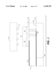
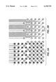
- FIG. 1 shows a typical two surface routing scheme for a PWB.
- a plurality of ball pads 10 serves to electrically couple a PWB 12 with a plurality of solder balls 14 on a ball grid array (BGA) package 16.
- the PWB comprises a substrate with two surfaces, 18 and 20, which are located on first and second planes, 19 and 21, which are parallel to one another.
- the plurality of ball pads 10 are on surface 18.
- a first group 20 of the plurality of ball pads 10 is routed by traces 22 on surface 18 while a second group 24 of the plurality of ball pads 10 is routed by traces 26 on surface 20.
- Each of a plurality of short traces 29 (see FIG. 2a) electrically couples a corresponding one of the second group 24 with a corresponding one of a plurality of vias 28, which in turn is connected to a corresponding one of the traces 26 on surface 20.
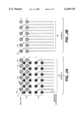
- FIGS. 2a and 2b spacing constraints between traces prevent all the plurality of solder ball pads 10 from being routed on the same surface; thus, the two (or more) level routing scheme is required for the that is routed as shown in FIGS. 2a and 2b.
- FIG. 2a shows the routing scheme for surface 18 while FIG. 2b shows the routing scheme for surface 20.
- the distance between the traces 22 must exceed a certain threshold. (The same holds true for the traces 26 in FIG. 2b). Therefore, given the area of surface 18, the second group of ball pads 24 could not be routed on surface 18.
- each of the vias 28 connects one of the second group of ball pads 24 to the traces 26 on surface 20.
- the vias 28 are arranged in a grid like structure; that is, the orientation between each of the vias 28 and its respective ball pad is constant.
- Each of a first group of electrical contacts such as bond pads is disposed on a first surface and is electrically coupled to one of a plurality of conductive surface connectors such as vias.
- Each of a second group of electrical contacts is disposed on the first surface and is routed by one of a second plurality of traces.
- Each of a plurality of short traces couple each of the bond pads in the first group with corresponding ones of the vias, which in turn are electrically coupled to one of a plurality of first traces on the second surface.
- the orientation between certain electrical contacts in the first group and their associated vias is different than the orientation between certain other electrical contacts in the first group and their associated vias. This varying orientation allows greater routing density on the second surface.
- FIG. 1 is a side view of a two layer PWB.
- FIGS. 2a and 2b respectively, show a conventional wire routing scheme for each of the two layers of the PWB shown in FIG. 1.
- FIGS. 3a and 3b respectively, show a wire routing scheme according to an embodiment of the present invention for each of the two layers of the PWB shown in FIG. 1.
- FIG. 4 is a simplified view of a portion of FIG. 3a, illustrating some of the geometrical relationships between electrical contacts and corresponding vias.
- FIGS. 5a and 5b respectively, show a wire routing scheme according to an alternate embodiment of the present invention for each of the two layers of the PWB shown in FIG. 1.
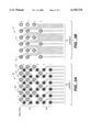
- FIGS. 3a and 3b respectively, show a routing schemes for a first surface 30 and a second surface 31 of a two surface PWB such as that shown in FIG. 1.
- the first surface 30 and the second surface 31, respectively lie on planes 39 and 41, respectively; in the preferred embodiment, planes 39 and 41 are parallel to one another since these planes correspond to planes 19 and 21 of FIG. 1.
- PWB routing for example, without limitation, ball grid array routing.
- each of a first group of electrical contacts (bond pads) 32 is electrically coupled to one of a plurality of conductive surface connectors (vias) 34.
- Each of a second group of electrical contacts (bond pads) 36 is routed by one of a second plurality of traces 38.
- Each of a plurality of short traces 35 couple each of the bond pads in the first group 32 with a corresponding one of the vias 34, which in turn is electrically coupled to a corresponding one of a plurality of first traces 40 on the second surface 32.
- the vias 34 need not end on the same surface; that is, different groups' vias 34 could connect to a corresponding one of a plurality of surfaces. This scheme would make sense, for example, in a PWB with surfaces having different surface areas.
- the bond pads 32 are arranged in a grid of evenly spaced rows and columns comprising rows 1 through 5 and columns 1-6. (It will be appreciated, however, that the present invention is not limited to grid type layouts).
- rows 1 and 2 the orientation between each of the vias 34 and its corresponding one of the bond pads 32 is identical.
- row 3 the orientation of the vias 34 in columns 1, 3, and 5 is different than the orientation of the vias in columns 2, 4 and 6.
- This altered orientation results in a greater pitch (distance) between certain of the vias 34 which in turn means that more of the first plurality of traces 40 may be routed between these vias 34.
- two traces, 40a and 40b may be routed between vias 34a and 34b.
- This extra spacing allows an extra row (row 3) of bond pads 32 to be routed in the second surface 21, compared with the prior art technique as shown in FIGS. 2a and 2b (assuming that the PWB surface area in those Figures is the same as the surface are of the PWB shown in FIGS. 3a and 3b).
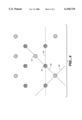
- FIG. 4 shows the geometrical features of the layout of FIG. 3a.
- FIG. 4 shows columns 1-3 of rows 3 and 4 of FIG. 3a; the remaining rows and columns have been omitted for the purposes of illustration.
- electrical contacts that are a subset of the first group of electrical contacts 32 and each of the plurality of vias 34 has a geometric center located a corresponding point on the first surface 30, shown as points 52 and 54 respectively.
- the geometric center of a bond pad and its associated vias defines a line, such as line 56 or line 58.
- Lines corresponding to bond pads in columns 2, 4, and 6 of row 3 are all parallel to one another and intersect lines corresponding to bond pads in columns 1, 3, and 5 of row 3 (fourth group of bond pads) at an angle of 90 degrees, which is shown in FIG. 4 as the angle between the intersection of line 56 and line 58.
- lines corresponding to the third group of bond pads 52, such as line 56 intersect any line, such as line 60, parallel to row 3 (i.e. a line that passes through the geometric center of the bond pads in row 3) at an angle of 45 degrees.
- Lines corresponding to bond pads in the fourth group of bond pads 54, such as line 58 intersect any line parallel to row 3 at an angle of -45 degrees.
- FIGS. 5a and 5b respectively, show first and second surfaces, routed in accordance with a preferred embodiment of the present invention, for a 6 ⁇ 8 array of bond pads.
Abstract
Description
Claims (11)
Priority Applications (1)
| Application Number | Priority Date | Filing Date | Title |
|---|---|---|---|
| US09/345,432 US6150729A (en) | 1999-07-01 | 1999-07-01 | Routing density enhancement for semiconductor BGA packages and printed wiring boards |
Applications Claiming Priority (1)
| Application Number | Priority Date | Filing Date | Title |
|---|---|---|---|
| US09/345,432 US6150729A (en) | 1999-07-01 | 1999-07-01 | Routing density enhancement for semiconductor BGA packages and printed wiring boards |
Publications (1)
| Publication Number | Publication Date |
|---|---|
| US6150729A true US6150729A (en) | 2000-11-21 |
Family
ID=23355025
Family Applications (1)
| Application Number | Title | Priority Date | Filing Date |
|---|---|---|---|
| US09/345,432 Expired - Lifetime US6150729A (en) | 1999-07-01 | 1999-07-01 | Routing density enhancement for semiconductor BGA packages and printed wiring boards |
Country Status (1)
| Country | Link |
|---|---|
| US (1) | US6150729A (en) |
Cited By (32)
| Publication number | Priority date | Publication date | Assignee | Title |
|---|---|---|---|---|
| KR20020023889A (en) * | 2001-12-27 | 2002-03-29 | 박종선 | BGA printed circuit board and the manufacturing method |
| EP1361612A2 (en) * | 2002-05-07 | 2003-11-12 | Kabushiki Kaisha Toshiba | Organic substrate for flip chip bonding |
| US6664483B2 (en) * | 2001-05-15 | 2003-12-16 | Intel Corporation | Electronic package with high density interconnect and associated methods |
| US20040164427A1 (en) * | 2003-02-25 | 2004-08-26 | Broadcom Corporation | Optimization of routing layers and board space requirements for ball grid array package implementations including array corner considerations |
| US20040164431A1 (en) * | 2003-02-25 | 2004-08-26 | Broadcom Corporation | Optimization of routing layers and board space requirements for ball grid array package implementations including single and multi-layer routing |
| US20050014395A1 (en) * | 2003-01-13 | 2005-01-20 | Fjelstad Joseph C. | System for making high-speed connections to board-mounted modules |
| EP1515366A2 (en) * | 2003-09-09 | 2005-03-16 | Nortel Networks Limited | Techniques for pad arrangements on circuit chips |
| US6891272B1 (en) | 2002-07-31 | 2005-05-10 | Silicon Pipe, Inc. | Multi-path via interconnection structures and methods for manufacturing the same |
| WO2005076677A1 (en) * | 2004-02-04 | 2005-08-18 | Koninklijke Philips Electronics, N.V. | Method for increasing a routing density for a circuit board and such a circuit board |
| WO2006053891A1 (en) * | 2004-11-19 | 2006-05-26 | Alcatel Lucent | Off-width pitch for improved circuit card routing |
| WO2006056473A2 (en) * | 2004-11-29 | 2006-06-01 | Fci | Improved matched-impedance surface-mount technology footprints |
| US20060231833A1 (en) * | 2004-11-29 | 2006-10-19 | Fci Americas Technology, Inc. | High-Frequency, High-Signal-Density, Surface-Mount Technology Footprint Definitions |
| US20060232301A1 (en) * | 2004-11-29 | 2006-10-19 | Fci Americas Technology, Inc. | Matched-impedance surface-mount technology footprints |
| US7307293B2 (en) | 2002-04-29 | 2007-12-11 | Silicon Pipe, Inc. | Direct-connect integrated circuit signaling system for bypassing intra-substrate printed circuit signal paths |
| US20080017971A1 (en) * | 2006-07-21 | 2008-01-24 | Bae Systems Information And Electronic Systems Integration Inc. | High speed, high density, low power die interconnect system |
| US20080178139A1 (en) * | 2006-11-08 | 2008-07-24 | Pfeil Charles L | Use of breakouts in printed circuit board designs |
| US20080185181A1 (en) * | 2006-11-08 | 2008-08-07 | Pfeil Charles L | Alternating via fanout patterns |
| US20090115072A1 (en) * | 2007-11-01 | 2009-05-07 | Texas Instruments Incorporated | BGA Package with Traces for Plating Pads Under the Chip |
| US20090178829A1 (en) * | 2008-01-15 | 2009-07-16 | Wintex Corporation | Anti-breakage structure for transmitting end formed on flexible printed circuitboard |
| US7708569B2 (en) | 2006-10-30 | 2010-05-04 | Fci Americas Technology, Inc. | Broadside-coupled signal pair configurations for electrical connectors |
| US7713088B2 (en) | 2006-10-05 | 2010-05-11 | Fci | Broadside-coupled signal pair configurations for electrical connectors |
| US7750446B2 (en) | 2002-04-29 | 2010-07-06 | Interconnect Portfolio Llc | IC package structures having separate circuit interconnection structures and assemblies constructed thereof |
| US7837505B2 (en) | 2006-08-21 | 2010-11-23 | Fci Americas Technology Llc | Electrical connector system with jogged contact tails |
| US7837504B2 (en) | 2003-09-26 | 2010-11-23 | Fci Americas Technology, Inc. | Impedance mating interface for electrical connectors |
| CN101932207A (en) * | 2010-09-06 | 2010-12-29 | 创扬通信技术(深圳)有限公司 | Multilayer PCB (Printed Circuit Board) and design method thereof |
| US20130215588A1 (en) * | 2012-02-21 | 2013-08-22 | Fujitsu Limited | Multilayered wiring substrate and electronic apparatus |
| CN103500717A (en) * | 2013-10-23 | 2014-01-08 | 青岛歌尔声学科技有限公司 | Layout method for PCB (Printed Circuit Board) mounted with BGA (Ball Grid Array) chip and PCB prepared by applying same |
| US8715003B2 (en) | 2009-12-30 | 2014-05-06 | Fci Americas Technology Llc | Electrical connector having impedance tuning ribs |
| US9136634B2 (en) | 2010-09-03 | 2015-09-15 | Fci Americas Technology Llc | Low-cross-talk electrical connector |
| CN107251663A (en) * | 2015-02-12 | 2017-10-13 | 古河电气工业株式会社 | Flexible base board and optical module |
| US20190239338A1 (en) * | 2018-01-29 | 2019-08-01 | Hewlett Packard Enterprise Development Lp | Single ended vias with shared voids |
| US20200083155A1 (en) * | 2018-09-11 | 2020-03-12 | Intel Corporation | Electrical routing component layout for crosstalk reduction |
Citations (7)
| Publication number | Priority date | Publication date | Assignee | Title |
|---|---|---|---|---|
| US5450290A (en) * | 1993-02-01 | 1995-09-12 | International Business Machines Corporation | Printed circuit board with aligned connections and method of making same |
| US5625944A (en) * | 1992-12-30 | 1997-05-06 | Interconnect Systems, Inc. | Methods for interconnecting integrated circuits |
| US5650660A (en) * | 1995-12-20 | 1997-07-22 | Intel Corp | Circuit pattern for a ball grid array integrated circuit package |
| US5686764A (en) * | 1996-03-20 | 1997-11-11 | Lsi Logic Corporation | Flip chip package with reduced number of package layers |
| US5686699A (en) * | 1995-10-10 | 1997-11-11 | Acc Microelectronics Corporation | Semiconductor board providing high signal pin utilization |
| US5903051A (en) * | 1998-04-03 | 1999-05-11 | Motorola, Inc. | Electronic component and method of manufacture |
| US6008543A (en) * | 1995-03-09 | 1999-12-28 | Sony Corporation | Conductive bumps on pads for flip chip application |
-
1999
- 1999-07-01 US US09/345,432 patent/US6150729A/en not_active Expired - Lifetime
Patent Citations (7)
| Publication number | Priority date | Publication date | Assignee | Title |
|---|---|---|---|---|
| US5625944A (en) * | 1992-12-30 | 1997-05-06 | Interconnect Systems, Inc. | Methods for interconnecting integrated circuits |
| US5450290A (en) * | 1993-02-01 | 1995-09-12 | International Business Machines Corporation | Printed circuit board with aligned connections and method of making same |
| US6008543A (en) * | 1995-03-09 | 1999-12-28 | Sony Corporation | Conductive bumps on pads for flip chip application |
| US5686699A (en) * | 1995-10-10 | 1997-11-11 | Acc Microelectronics Corporation | Semiconductor board providing high signal pin utilization |
| US5650660A (en) * | 1995-12-20 | 1997-07-22 | Intel Corp | Circuit pattern for a ball grid array integrated circuit package |
| US5686764A (en) * | 1996-03-20 | 1997-11-11 | Lsi Logic Corporation | Flip chip package with reduced number of package layers |
| US5903051A (en) * | 1998-04-03 | 1999-05-11 | Motorola, Inc. | Electronic component and method of manufacture |
Cited By (74)
| Publication number | Priority date | Publication date | Assignee | Title |
|---|---|---|---|---|
| US6664483B2 (en) * | 2001-05-15 | 2003-12-16 | Intel Corporation | Electronic package with high density interconnect and associated methods |
| KR20020023889A (en) * | 2001-12-27 | 2002-03-29 | 박종선 | BGA printed circuit board and the manufacturing method |
| US7750446B2 (en) | 2002-04-29 | 2010-07-06 | Interconnect Portfolio Llc | IC package structures having separate circuit interconnection structures and assemblies constructed thereof |
| US7307293B2 (en) | 2002-04-29 | 2007-12-11 | Silicon Pipe, Inc. | Direct-connect integrated circuit signaling system for bypassing intra-substrate printed circuit signal paths |
| US7989929B2 (en) | 2002-04-29 | 2011-08-02 | Samsung Electronics Co., Ltd. | Direct-connect signaling system |
| EP1361612A2 (en) * | 2002-05-07 | 2003-11-12 | Kabushiki Kaisha Toshiba | Organic substrate for flip chip bonding |
| US6768206B2 (en) * | 2002-05-07 | 2004-07-27 | Kabushiki Kaisha Toshiba | Organic substrate for flip chip bonding |
| EP1361612A3 (en) * | 2002-05-07 | 2006-05-17 | Kabushiki Kaisha Toshiba | Organic substrate for flip chip bonding |
| US6891272B1 (en) | 2002-07-31 | 2005-05-10 | Silicon Pipe, Inc. | Multi-path via interconnection structures and methods for manufacturing the same |
| US20050014395A1 (en) * | 2003-01-13 | 2005-01-20 | Fjelstad Joseph C. | System for making high-speed connections to board-mounted modules |
| US7014472B2 (en) | 2003-01-13 | 2006-03-21 | Siliconpipe, Inc. | System for making high-speed connections to board-mounted modules |
| US20050016749A1 (en) * | 2003-02-25 | 2005-01-27 | Broadcom Corporation | Method and system for optimizing routing layers and board space requirements for a ball grid array land pattern |
| US7855448B2 (en) | 2003-02-25 | 2010-12-21 | Broadcom Corporation | Optimization of routing layers and board space requirements for ball grid array package implementations including array corner considerations |
| US20040164427A1 (en) * | 2003-02-25 | 2004-08-26 | Broadcom Corporation | Optimization of routing layers and board space requirements for ball grid array package implementations including array corner considerations |
| US7005753B2 (en) | 2003-02-25 | 2006-02-28 | Broadcom Corporation | Optimization of routing layers and board space requirements for a ball grid array land pattern |
| US7009115B2 (en) | 2003-02-25 | 2006-03-07 | Broadcom Corporation | Optimization of routing layers and board space requirements for a ball grid array package |
| US20050077634A1 (en) * | 2003-02-25 | 2005-04-14 | Seaman Kevin L. | Optimization of routing layers and board space requirements for a ball grid array package |
| US20050077625A1 (en) * | 2003-02-25 | 2005-04-14 | Broadcom Corporation | Optimization of routing layers and board space requirements for a ball grid array land pattern |
| US7816247B2 (en) | 2003-02-25 | 2010-10-19 | Broadcom Corporation | Optimization of routing layers and board space requirements for ball grid array package implementations including array corner considerations |
| US8695212B2 (en) | 2003-02-25 | 2014-04-15 | Broad Corporation | Method for optimizing routing layers and board space requirements for a ball grid array land pattern |
| US6916995B2 (en) * | 2003-02-25 | 2005-07-12 | Broadcom Corporation | Optimization of routing layers and board space requirements for ball grid array package implementations including single and multi-layer routing |
| US20040164431A1 (en) * | 2003-02-25 | 2004-08-26 | Broadcom Corporation | Optimization of routing layers and board space requirements for ball grid array package implementations including single and multi-layer routing |
| EP1515366A2 (en) * | 2003-09-09 | 2005-03-16 | Nortel Networks Limited | Techniques for pad arrangements on circuit chips |
| EP1515366A3 (en) * | 2003-09-09 | 2007-03-21 | Nortel Networks Limited | Techniques for pad arrangements on circuit chips |
| US7837504B2 (en) | 2003-09-26 | 2010-11-23 | Fci Americas Technology, Inc. | Impedance mating interface for electrical connectors |
| US20080251286A1 (en) * | 2004-02-04 | 2008-10-16 | Koninklijke Philips Electronics N.V. | Method For Increasing a Routing Density For a Circuit Board and Such a Circuit Board |
| WO2005076677A1 (en) * | 2004-02-04 | 2005-08-18 | Koninklijke Philips Electronics, N.V. | Method for increasing a routing density for a circuit board and such a circuit board |
| WO2006053891A1 (en) * | 2004-11-19 | 2006-05-26 | Alcatel Lucent | Off-width pitch for improved circuit card routing |
| CN101673886B (en) * | 2004-11-29 | 2012-07-25 | Fci公司 | Improved matched-impedance surface-mount technology footprints |
| CN101112135B (en) * | 2004-11-29 | 2010-12-29 | Fci公司 | Improved matched-impedance surface-mount technology footprints |
| WO2006056473A2 (en) * | 2004-11-29 | 2006-06-01 | Fci | Improved matched-impedance surface-mount technology footprints |
| US8383951B2 (en) | 2004-11-29 | 2013-02-26 | Fci | Matched-impedance connector footprints |
| US20100041256A1 (en) * | 2004-11-29 | 2010-02-18 | Fci Americas Technology, Inc. | Matched-Impedance Connector Footprints |
| US20100041275A1 (en) * | 2004-11-29 | 2010-02-18 | Fci Americas Technology, Inc. | Matched-Impedance Connector Footprints |
| US20100048043A1 (en) * | 2004-11-29 | 2010-02-25 | Fci Americas Technology, Inc. | Matched-Impedance Connector Footprints |
| US7709747B2 (en) | 2004-11-29 | 2010-05-04 | Fci | Matched-impedance surface-mount technology footprints |
| WO2006056473A3 (en) * | 2004-11-29 | 2006-09-08 | Framatome Connectors Int | Improved matched-impedance surface-mount technology footprints |
| CN101673885B (en) * | 2004-11-29 | 2012-07-18 | Fci公司 | Improved matched-impedance surface-mount technology footprints |
| US8183466B2 (en) | 2004-11-29 | 2012-05-22 | Fci | Matched-impedance connector footprints |
| CN101674707B (en) * | 2004-11-29 | 2012-02-22 | Fci公司 | Improved matched-impedance surface-mount technology footprints |
| US20060231833A1 (en) * | 2004-11-29 | 2006-10-19 | Fci Americas Technology, Inc. | High-Frequency, High-Signal-Density, Surface-Mount Technology Footprint Definitions |
| US7284221B2 (en) | 2004-11-29 | 2007-10-16 | Fci Americas Technology, Inc. | High-frequency, high-signal-density, surface-mount technology footprint definitions |
| US20060232301A1 (en) * | 2004-11-29 | 2006-10-19 | Fci Americas Technology, Inc. | Matched-impedance surface-mount technology footprints |
| US7935896B2 (en) | 2004-11-29 | 2011-05-03 | Fci | Matched-impedance connector footprints |
| US8426968B2 (en) | 2006-07-21 | 2013-04-23 | Sagacious Investment Group L.L.C. | High speed, high density, low power die interconnect system |
| US9905461B2 (en) | 2006-07-21 | 2018-02-27 | Gula Consulting Limited Liability Company | High speed, high density, low power die interconnect system |
| US7999383B2 (en) | 2006-07-21 | 2011-08-16 | Bae Systems Information And Electronic Systems Integration Inc. | High speed, high density, low power die interconnect system |
| US9324658B2 (en) | 2006-07-21 | 2016-04-26 | Gula Consulting Limited Liability Company | High speed, high density, low power die interconnect system |
| US11069571B2 (en) | 2006-07-21 | 2021-07-20 | Gula Consulting Limited Liability Company | High speed, high density, low power die interconnect system |
| US20080017971A1 (en) * | 2006-07-21 | 2008-01-24 | Bae Systems Information And Electronic Systems Integration Inc. | High speed, high density, low power die interconnect system |
| US10872816B2 (en) | 2006-07-21 | 2020-12-22 | Gula Consulting Limited Liabiity Company | High speed, high density, low power die interconnect system |
| US9917008B2 (en) | 2006-07-21 | 2018-03-13 | Gula Consulting Limited Liability Company | High speed, high density, low power die interconnect system |
| US9922873B2 (en) | 2006-07-21 | 2018-03-20 | Gula Consulting Limited Liability Company | High speed, high density, low power die interconnect system |
| US8426244B2 (en) | 2006-07-21 | 2013-04-23 | Sagacious Investment Group L.L.C. | High speed, high density, low power die interconnect system |
| US9240382B2 (en) | 2006-07-21 | 2016-01-19 | Sagacious Investment Group, L.L.C. | High speed, high density, low power die interconnect system |
| US7837505B2 (en) | 2006-08-21 | 2010-11-23 | Fci Americas Technology Llc | Electrical connector system with jogged contact tails |
| US7713088B2 (en) | 2006-10-05 | 2010-05-11 | Fci | Broadside-coupled signal pair configurations for electrical connectors |
| US7708569B2 (en) | 2006-10-30 | 2010-05-04 | Fci Americas Technology, Inc. | Broadside-coupled signal pair configurations for electrical connectors |
| US20080185181A1 (en) * | 2006-11-08 | 2008-08-07 | Pfeil Charles L | Alternating via fanout patterns |
| US20080178139A1 (en) * | 2006-11-08 | 2008-07-24 | Pfeil Charles L | Use of breakouts in printed circuit board designs |
| US8103988B2 (en) | 2006-11-08 | 2012-01-24 | Mentor Graphics Corporation | Use of breakouts in printed circuit board designs |
| US20090115072A1 (en) * | 2007-11-01 | 2009-05-07 | Texas Instruments Incorporated | BGA Package with Traces for Plating Pads Under the Chip |
| US8053349B2 (en) | 2007-11-01 | 2011-11-08 | Texas Instruments Incorporated | BGA package with traces for plating pads under the chip |
| US20090178829A1 (en) * | 2008-01-15 | 2009-07-16 | Wintex Corporation | Anti-breakage structure for transmitting end formed on flexible printed circuitboard |
| US8715003B2 (en) | 2009-12-30 | 2014-05-06 | Fci Americas Technology Llc | Electrical connector having impedance tuning ribs |
| US9136634B2 (en) | 2010-09-03 | 2015-09-15 | Fci Americas Technology Llc | Low-cross-talk electrical connector |
| CN101932207B (en) * | 2010-09-06 | 2012-02-29 | 创扬通信技术(深圳)有限公司 | Multilayer PCB (Printed Circuit Board) and design method thereof |
| CN101932207A (en) * | 2010-09-06 | 2010-12-29 | 创扬通信技术(深圳)有限公司 | Multilayer PCB (Printed Circuit Board) and design method thereof |
| US20130215588A1 (en) * | 2012-02-21 | 2013-08-22 | Fujitsu Limited | Multilayered wiring substrate and electronic apparatus |
| CN103500717A (en) * | 2013-10-23 | 2014-01-08 | 青岛歌尔声学科技有限公司 | Layout method for PCB (Printed Circuit Board) mounted with BGA (Ball Grid Array) chip and PCB prepared by applying same |
| CN107251663A (en) * | 2015-02-12 | 2017-10-13 | 古河电气工业株式会社 | Flexible base board and optical module |
| US20190239338A1 (en) * | 2018-01-29 | 2019-08-01 | Hewlett Packard Enterprise Development Lp | Single ended vias with shared voids |
| US10477672B2 (en) * | 2018-01-29 | 2019-11-12 | Hewlett Packard Enterprise Development Lp | Single ended vias with shared voids |
| US20200083155A1 (en) * | 2018-09-11 | 2020-03-12 | Intel Corporation | Electrical routing component layout for crosstalk reduction |
Similar Documents
| Publication | Publication Date | Title |
|---|---|---|
| US6150729A (en) | Routing density enhancement for semiconductor BGA packages and printed wiring boards | |
| US10804139B2 (en) | Semiconductor system | |
| US8039320B2 (en) | Optimized circuit design layout for high performance ball grid array packages | |
| US5847936A (en) | Optimized routing scheme for an integrated circuit/printed circuit board | |
| US6976848B2 (en) | Sockets for module extension and memory system using same | |
| US7456505B2 (en) | Integrated circuit chip and integrated device | |
| US6373139B1 (en) | Layout for a ball grid array | |
| US6011695A (en) | External bus interface printed circuit board routing for a ball grid array integrated circuit package | |
| US20020086459A1 (en) | Circuit mounting method, circuit mounted board, and semiconductor device | |
| US7095107B2 (en) | Ball assignment schemes for integrated circuit packages | |
| US6534872B1 (en) | Apparatus and system with increased signal trace routing options in printed wiring boards and integrated circuit packaging | |
| US6831233B2 (en) | Chip package with degassing holes | |
| US20020038724A1 (en) | Chip scale package, printed circuit board, and method of designing a piinted circuit board | |
| US6664620B2 (en) | Integrated circuit die and/or package having a variable pitch contact array for maximization of number of signal lines per routing layer | |
| US6777815B2 (en) | Configuration of conductive bumps and redistribution layer on a flip chip | |
| US5691569A (en) | Integrated circuit package that has a plurality of staggered pins | |
| US6662250B1 (en) | Optimized routing strategy for multiple synchronous bus groups | |
| US11812544B2 (en) | Breakout structure for an integrated circuit device | |
| US6945791B2 (en) | Integrated circuit redistribution package | |
| KR100725517B1 (en) | multi-layered circuit substrate having bonding pads and ball lands arranged on two or more layers, and semiconductor package structure using the same | |
| KR102578797B1 (en) | Semiconductor package | |
| US6603200B1 (en) | Integrated circuit package | |
| CN116487359A (en) | Semiconductor package | |
| JP2002164474A (en) | Chip scale package, circuit board, electronic module and method for designing circuit board | |
| JPH08181250A (en) | Semiconductor package |
Legal Events
| Date | Code | Title | Description |
|---|---|---|---|
| AS | Assignment |
Owner name: LSI LOGIC CORPORATION, CALIFORNIA Free format text: ASSIGNMENT OF ASSIGNORS INTEREST;ASSIGNOR:GHAHGHAHI, FARSHAD;REEL/FRAME:010093/0543 Effective date: 19990630 |
|
| STCF | Information on status: patent grant |
Free format text: PATENTED CASE |
|
| FPAY | Fee payment |
Year of fee payment: 4 |
|
| FEPP | Fee payment procedure |
Free format text: PAYOR NUMBER ASSIGNED (ORIGINAL EVENT CODE: ASPN); ENTITY STATUS OF PATENT OWNER: LARGE ENTITY Free format text: PAYER NUMBER DE-ASSIGNED (ORIGINAL EVENT CODE: RMPN); ENTITY STATUS OF PATENT OWNER: LARGE ENTITY |
|
| FPAY | Fee payment |
Year of fee payment: 8 |
|
| FPAY | Fee payment |
Year of fee payment: 12 |
|
| AS | Assignment |
Owner name: DEUTSCHE BANK AG NEW YORK BRANCH, AS COLLATERAL AG Free format text: PATENT SECURITY AGREEMENT;ASSIGNORS:LSI CORPORATION;AGERE SYSTEMS LLC;REEL/FRAME:032856/0031 Effective date: 20140506 |
|
| AS | Assignment |
Owner name: LSI CORPORATION, CALIFORNIA Free format text: CHANGE OF NAME;ASSIGNOR:LSI LOGIC CORPORATION;REEL/FRAME:033102/0270 Effective date: 20070406 |
|
| AS | Assignment |
Owner name: AVAGO TECHNOLOGIES GENERAL IP (SINGAPORE) PTE. LTD Free format text: ASSIGNMENT OF ASSIGNORS INTEREST;ASSIGNOR:LSI CORPORATION;REEL/FRAME:035390/0388 Effective date: 20140814 |
|
| AS | Assignment |
Owner name: LSI CORPORATION, CALIFORNIA Free format text: TERMINATION AND RELEASE OF SECURITY INTEREST IN PATENT RIGHTS (RELEASES RF 032856-0031);ASSIGNOR:DEUTSCHE BANK AG NEW YORK BRANCH, AS COLLATERAL AGENT;REEL/FRAME:037684/0039 Effective date: 20160201 Owner name: AGERE SYSTEMS LLC, PENNSYLVANIA Free format text: TERMINATION AND RELEASE OF SECURITY INTEREST IN PATENT RIGHTS (RELEASES RF 032856-0031);ASSIGNOR:DEUTSCHE BANK AG NEW YORK BRANCH, AS COLLATERAL AGENT;REEL/FRAME:037684/0039 Effective date: 20160201 |
|
| AS | Assignment |
Owner name: BANK OF AMERICA, N.A., AS COLLATERAL AGENT, NORTH CAROLINA Free format text: PATENT SECURITY AGREEMENT;ASSIGNOR:AVAGO TECHNOLOGIES GENERAL IP (SINGAPORE) PTE. LTD.;REEL/FRAME:037808/0001 Effective date: 20160201 Owner name: BANK OF AMERICA, N.A., AS COLLATERAL AGENT, NORTH Free format text: PATENT SECURITY AGREEMENT;ASSIGNOR:AVAGO TECHNOLOGIES GENERAL IP (SINGAPORE) PTE. LTD.;REEL/FRAME:037808/0001 Effective date: 20160201 |
|
| AS | Assignment |
Owner name: AVAGO TECHNOLOGIES GENERAL IP (SINGAPORE) PTE. LTD., SINGAPORE Free format text: TERMINATION AND RELEASE OF SECURITY INTEREST IN PATENTS;ASSIGNOR:BANK OF AMERICA, N.A., AS COLLATERAL AGENT;REEL/FRAME:041710/0001 Effective date: 20170119 Owner name: AVAGO TECHNOLOGIES GENERAL IP (SINGAPORE) PTE. LTD Free format text: TERMINATION AND RELEASE OF SECURITY INTEREST IN PATENTS;ASSIGNOR:BANK OF AMERICA, N.A., AS COLLATERAL AGENT;REEL/FRAME:041710/0001 Effective date: 20170119 |
|
| AS | Assignment |
Owner name: BELL SEMICONDUCTOR, LLC, ILLINOIS Free format text: ASSIGNMENT OF ASSIGNORS INTEREST;ASSIGNORS:AVAGO TECHNOLOGIES GENERAL IP (SINGAPORE) PTE. LTD.;BROADCOM CORPORATION;REEL/FRAME:044886/0766 Effective date: 20171208 |
|
| AS | Assignment |
Owner name: CORTLAND CAPITAL MARKET SERVICES LLC, AS COLLATERA Free format text: SECURITY INTEREST;ASSIGNORS:HILCO PATENT ACQUISITION 56, LLC;BELL SEMICONDUCTOR, LLC;BELL NORTHERN RESEARCH, LLC;REEL/FRAME:045216/0020 Effective date: 20180124 |
|
| AS | Assignment |
Owner name: BELL NORTHERN RESEARCH, LLC, ILLINOIS Free format text: RELEASE BY SECURED PARTY;ASSIGNOR:CORTLAND CAPITAL MARKET SERVICES LLC;REEL/FRAME:059723/0382 Effective date: 20220401 Owner name: BELL SEMICONDUCTOR, LLC, ILLINOIS Free format text: RELEASE BY SECURED PARTY;ASSIGNOR:CORTLAND CAPITAL MARKET SERVICES LLC;REEL/FRAME:059723/0382 Effective date: 20220401 Owner name: HILCO PATENT ACQUISITION 56, LLC, ILLINOIS Free format text: RELEASE BY SECURED PARTY;ASSIGNOR:CORTLAND CAPITAL MARKET SERVICES LLC;REEL/FRAME:059723/0382 Effective date: 20220401 |