EP1515366A2 - Techniques for pad arrangements on circuit chips - Google Patents
Techniques for pad arrangements on circuit chips Download PDFInfo
- Publication number
- EP1515366A2 EP1515366A2 EP04394053A EP04394053A EP1515366A2 EP 1515366 A2 EP1515366 A2 EP 1515366A2 EP 04394053 A EP04394053 A EP 04394053A EP 04394053 A EP04394053 A EP 04394053A EP 1515366 A2 EP1515366 A2 EP 1515366A2
- Authority
- EP
- European Patent Office
- Prior art keywords
- channels
- electrical contacts
- circuit chip
- circuit
- chip
- Prior art date
- Legal status (The legal status is an assumption and is not a legal conclusion. Google has not performed a legal analysis and makes no representation as to the accuracy of the status listed.)
- Withdrawn
Links
Images


Classifications
-
- H—ELECTRICITY
- H05—ELECTRIC TECHNIQUES NOT OTHERWISE PROVIDED FOR
- H05K—PRINTED CIRCUITS; CASINGS OR CONSTRUCTIONAL DETAILS OF ELECTRIC APPARATUS; MANUFACTURE OF ASSEMBLAGES OF ELECTRICAL COMPONENTS
- H05K1/00—Printed circuits
- H05K1/02—Details
- H05K1/11—Printed elements for providing electric connections to or between printed circuits
- H05K1/111—Pads for surface mounting, e.g. lay-out
- H05K1/112—Pads for surface mounting, e.g. lay-out directly combined with via connections
-
- H—ELECTRICITY
- H05—ELECTRIC TECHNIQUES NOT OTHERWISE PROVIDED FOR
- H05K—PRINTED CIRCUITS; CASINGS OR CONSTRUCTIONAL DETAILS OF ELECTRIC APPARATUS; MANUFACTURE OF ASSEMBLAGES OF ELECTRICAL COMPONENTS
- H05K1/00—Printed circuits
- H05K1/02—Details
- H05K1/11—Printed elements for providing electric connections to or between printed circuits
- H05K1/115—Via connections; Lands around holes or via connections
-
- H10W70/65—
-
- H—ELECTRICITY
- H05—ELECTRIC TECHNIQUES NOT OTHERWISE PROVIDED FOR
- H05K—PRINTED CIRCUITS; CASINGS OR CONSTRUCTIONAL DETAILS OF ELECTRIC APPARATUS; MANUFACTURE OF ASSEMBLAGES OF ELECTRICAL COMPONENTS
- H05K1/00—Printed circuits
- H05K1/02—Details
- H05K1/0296—Conductive pattern lay-out details not covered by sub groups H05K1/02 - H05K1/0295
- H05K1/0298—Multilayer circuits
-
- H—ELECTRICITY
- H05—ELECTRIC TECHNIQUES NOT OTHERWISE PROVIDED FOR
- H05K—PRINTED CIRCUITS; CASINGS OR CONSTRUCTIONAL DETAILS OF ELECTRIC APPARATUS; MANUFACTURE OF ASSEMBLAGES OF ELECTRICAL COMPONENTS
- H05K2201/00—Indexing scheme relating to printed circuits covered by H05K1/00
- H05K2201/09—Shape and layout
- H05K2201/09209—Shape and layout details of conductors
- H05K2201/09218—Conductive traces
- H05K2201/09227—Layout details of a plurality of traces, e.g. escape layout for Ball Grid Array [BGA] mounting
-
- H—ELECTRICITY
- H05—ELECTRIC TECHNIQUES NOT OTHERWISE PROVIDED FOR
- H05K—PRINTED CIRCUITS; CASINGS OR CONSTRUCTIONAL DETAILS OF ELECTRIC APPARATUS; MANUFACTURE OF ASSEMBLAGES OF ELECTRICAL COMPONENTS
- H05K2201/00—Indexing scheme relating to printed circuits covered by H05K1/00
- H05K2201/09—Shape and layout
- H05K2201/09209—Shape and layout details of conductors
- H05K2201/09218—Conductive traces
- H05K2201/09236—Parallel layout
-
- H—ELECTRICITY
- H05—ELECTRIC TECHNIQUES NOT OTHERWISE PROVIDED FOR
- H05K—PRINTED CIRCUITS; CASINGS OR CONSTRUCTIONAL DETAILS OF ELECTRIC APPARATUS; MANUFACTURE OF ASSEMBLAGES OF ELECTRICAL COMPONENTS
- H05K2201/00—Indexing scheme relating to printed circuits covered by H05K1/00
- H05K2201/09—Shape and layout
- H05K2201/09209—Shape and layout details of conductors
- H05K2201/09218—Conductive traces
- H05K2201/09263—Meander
-
- H—ELECTRICITY
- H05—ELECTRIC TECHNIQUES NOT OTHERWISE PROVIDED FOR
- H05K—PRINTED CIRCUITS; CASINGS OR CONSTRUCTIONAL DETAILS OF ELECTRIC APPARATUS; MANUFACTURE OF ASSEMBLAGES OF ELECTRICAL COMPONENTS
- H05K2201/00—Indexing scheme relating to printed circuits covered by H05K1/00
- H05K2201/09—Shape and layout
- H05K2201/09209—Shape and layout details of conductors
- H05K2201/095—Conductive through-holes or vias
- H05K2201/09509—Blind vias, i.e. vias having one side closed
-
- H—ELECTRICITY
- H05—ELECTRIC TECHNIQUES NOT OTHERWISE PROVIDED FOR
- H05K—PRINTED CIRCUITS; CASINGS OR CONSTRUCTIONAL DETAILS OF ELECTRIC APPARATUS; MANUFACTURE OF ASSEMBLAGES OF ELECTRICAL COMPONENTS
- H05K2201/00—Indexing scheme relating to printed circuits covered by H05K1/00
- H05K2201/09—Shape and layout
- H05K2201/09209—Shape and layout details of conductors
- H05K2201/095—Conductive through-holes or vias
- H05K2201/09536—Buried plated through-holes, i.e. plated through-holes formed in a core before lamination
-
- H—ELECTRICITY
- H05—ELECTRIC TECHNIQUES NOT OTHERWISE PROVIDED FOR
- H05K—PRINTED CIRCUITS; CASINGS OR CONSTRUCTIONAL DETAILS OF ELECTRIC APPARATUS; MANUFACTURE OF ASSEMBLAGES OF ELECTRICAL COMPONENTS
- H05K2201/00—Indexing scheme relating to printed circuits covered by H05K1/00
- H05K2201/09—Shape and layout
- H05K2201/09209—Shape and layout details of conductors
- H05K2201/095—Conductive through-holes or vias
- H05K2201/09627—Special connections between adjacent vias, not for grounding vias
-
- H—ELECTRICITY
- H05—ELECTRIC TECHNIQUES NOT OTHERWISE PROVIDED FOR
- H05K—PRINTED CIRCUITS; CASINGS OR CONSTRUCTIONAL DETAILS OF ELECTRIC APPARATUS; MANUFACTURE OF ASSEMBLAGES OF ELECTRICAL COMPONENTS
- H05K2201/00—Indexing scheme relating to printed circuits covered by H05K1/00
- H05K2201/10—Details of components or other objects attached to or integrated in a printed circuit board
- H05K2201/10613—Details of electrical connections of non-printed components, e.g. special leads
- H05K2201/10621—Components characterised by their electrical contacts
- H05K2201/10674—Flip chip
-
- H—ELECTRICITY
- H05—ELECTRIC TECHNIQUES NOT OTHERWISE PROVIDED FOR
- H05K—PRINTED CIRCUITS; CASINGS OR CONSTRUCTIONAL DETAILS OF ELECTRIC APPARATUS; MANUFACTURE OF ASSEMBLAGES OF ELECTRICAL COMPONENTS
- H05K2201/00—Indexing scheme relating to printed circuits covered by H05K1/00
- H05K2201/10—Details of components or other objects attached to or integrated in a printed circuit board
- H05K2201/10613—Details of electrical connections of non-printed components, e.g. special leads
- H05K2201/10621—Components characterised by their electrical contacts
- H05K2201/10734—Ball grid array [BGA]; Bump grid array
-
- H—ELECTRICITY
- H05—ELECTRIC TECHNIQUES NOT OTHERWISE PROVIDED FOR
- H05K—PRINTED CIRCUITS; CASINGS OR CONSTRUCTIONAL DETAILS OF ELECTRIC APPARATUS; MANUFACTURE OF ASSEMBLAGES OF ELECTRICAL COMPONENTS
- H05K3/00—Apparatus or processes for manufacturing printed circuits
- H05K3/0005—Apparatus or processes for manufacturing printed circuits for designing circuits by computer
-
- H—ELECTRICITY
- H05—ELECTRIC TECHNIQUES NOT OTHERWISE PROVIDED FOR
- H05K—PRINTED CIRCUITS; CASINGS OR CONSTRUCTIONAL DETAILS OF ELECTRIC APPARATUS; MANUFACTURE OF ASSEMBLAGES OF ELECTRICAL COMPONENTS
- H05K3/00—Apparatus or processes for manufacturing printed circuits
- H05K3/40—Forming printed elements for providing electric connections to or between printed circuits
- H05K3/42—Plated through-holes or plated via connections
- H05K3/429—Plated through-holes specially for multilayer circuits, e.g. having connections to inner circuit layers
-
- H—ELECTRICITY
- H05—ELECTRIC TECHNIQUES NOT OTHERWISE PROVIDED FOR
- H05K—PRINTED CIRCUITS; CASINGS OR CONSTRUCTIONAL DETAILS OF ELECTRIC APPARATUS; MANUFACTURE OF ASSEMBLAGES OF ELECTRICAL COMPONENTS
- H05K3/00—Apparatus or processes for manufacturing printed circuits
- H05K3/46—Manufacturing multilayer circuits
- H05K3/4602—Manufacturing multilayer circuits characterized by a special circuit board as base or central core whereon additional circuit layers are built or additional circuit boards are laminated
-
- H10W72/20—
-
- H10W72/90—
-
- H10W72/9445—
-
- H10W90/701—
Definitions
- the present disclosure relates generally to circuit devices and, more particularly, to a technique for pin arrangement in a circuit chip.
- Circuit devices such as integrated circuits (ICs) typically are formed starting with a circuit chip, which typically includes circuit components arranged on and connected via a silicon chip substrate or similar dielectric material.
- the circuit chip further includes a contact pattern comprising electrical contacts positioned at a surface of the chip, where the electrical contacts serve to conduct signals (e.g., input/output or I/O) and power and ground input to and from the circuit chip.
- signals e.g., input/output or I/O
- the circuit chip typically is relatively fragile and because its contact pattern may not conform to standard contact patterns for interfacing with circuit board substrates or other devices, the circuit chip typically is mated with a chip package to enclose or envelop the circuit chip and to map the contact pattern of the circuit chip to a standard contact pattern (e.g., a contact pattern having a geometry that is typical of those used to interface with circuit board substrates).
- a standard contact pattern e.g., a contact pattern having a geometry that is typical of those used to interface with circuit board substrates.
- the chip package typically includes a plurality of routing layers and vias disposed therein that are used to route conductive traces from the electrical contacts of the contact pattern to their corresponding contacts of the chip package.
- circuit chip designers frequently design circuit chips in a manner that causes great difficulty for the designer of the corresponding chip package.
- a main goal of many circuit chip designers is to minimize the surface area, or "footprint,” of the circuit chip by achieving the highest density contact pattern possible.
- these high density footprints often result in an excessive number of routing layers in the chip package because the high density of contacts limits the number of electrical traces that may be routed via any given routing layer. Accordingly, this excessive number of routing layers results in an overall circuit device that is overly thick and therefore difficult to integrate into many systems as well as costly to manufacture.
- a technique may be realized as a circuit device comprising a circuit chip having a plurality of electrical contacts positioned at a surface of the circuit chip so as to form one or more channels at the surface of the circuit chip, wherein the one or more channels are substantially devoid of electrical contacts such that one or more corresponding channels are formed in a chip carrier for routing electrically conductive traces from one or more of the plurality of electrical contacts on a routing layer of the chip carrier.
- the circuit device may further beneficially comprise a chip carrier having at least one routing layer for routing electrically conductive traces from one or more of the plurality of electrical contacts toward a periphery of the chip carrier, wherein one or more conductive traces are routed via one or more channels in the at least one routing layer substantially corresponding to one or more of the plurality of channels at the surface of the circuit chip. If such is the case, the one or more channels in the at least one routing layer may beneficially be substantially devoid of vias.
- the plurality of electrical contacts may beneficially include a plurality of signal contacts and a plurality of power and ground contacts, wherein one or more of the plurality of signal contacts may beneficially be positioned at a periphery of the surface of the circuit chip and one or more of the plurality of power and ground contacts may beneficially be positioned at an interior of the surface of the circuit chip. If such is the case, one or more of the plurality of signal contacts may beneficially be positioned adjacent to at least one of the one or more channels.
- At least one of the one or more channels may beneficially extend from a periphery of the surface of the circuit chip into an interior of the surface of the circuit chip.
- a technique may be realized as a circuit device comprising a circuit chip having a plurality of power and ground electrical contacts and a plurality of signal electrical contacts positioned at a surface of the circuit chip, wherein a substantial portion of the plurality of power and ground electrical contacts are positioned at an interior of the surface of the circuit chip, and wherein a substantial portion of the plurality of signal electrical contacts are positioned at a periphery of the surface of the circuit chip.
- the plurality of power and ground electrical contacts and the plurality of signal electrical contacts may beneficially be positioned so as to form one or more channels at the surface of the circuit chip, wherein the one or more channels may beneficially be substantially devoid of electrical contacts such that one or more corresponding channels are formed in a chip carrier for routing electrically conductive traces from one or more of the plurality of electrical contacts on a routing layer of the chip carrier.
- the circuit device may further beneficially comprise a chip carrier having at least one routing layer for routing electrically conductive traces from one or more of the electrical contacts toward a periphery of the chip carrier, wherein one or more conductive traces may beneficially be routed via one or more channels in the at least one routing layer substantially corresponding to one or more of the plurality of channels at the surface of the circuit chip. Also, a substantial portion of the plurality of signal electrical contacts may beneficially be positioned adjacent to at least one of the one or more channels.
- a technique may be realized as a circuit device comprising a circuit chip having a plurality of electrical contacts positioned at a surface of the circuit chip, wherein a peripheral portion of the surface of the circuit chip has a first density of electrical contacts, wherein an interior portion of the surface of the circuit chip has a second density of electrical contacts, and wherein the second density is substantially less than the first density.
- the circuit chip may further beneficially comprise at least one thermal transfer contact positioned at the interior portion of the surface of the circuit chip.
- the plurality of electrical contacts may beneficially be positioned so as to form one or more channels at the surface of the circuit chip, wherein the one or more channels may beneficially be substantially devoid of electrical contacts such that one or more corresponding channels are formed in a chip carrier for routing electrically conductive traces from one or more of the plurality of electrical contacts on a routing layer of the chip carrier.
- the circuit device may further beneficially comprise a chip carrier having at least one routing layer for routing electrically conductive traces from one or more of the plurality of electrical contacts toward a periphery of the chip carrier, wherein one or more conductive traces may beneficially be routed via one or more channels in the at least one routing layer substantially corresponding to one or more of the plurality of channels at the surface of the circuit chip.
- a technique may be realized as a method comprising positioning a plurality of electrical contacts at a surface of a circuit chip so as to form one or more channels at the surface of the circuit chip, wherein the one or more channels are substantially clear of electrical contacts.
- the method also comprises forming one or more electrically conductive traces at one or more routing layers of a chip carrier supporting the circuit chip, wherein the one or more electrically conductive traces are routed from one or more of the plurality of electrical contacts toward a periphery of the chip carrier via one or more channels in the at least one routing layer substantially corresponding to one or more of the plurality of channels at the surface of the circuit chip.
- the one or more channels in the at least one routing layer of the chip carrier may beneficially be substantially devoid of vias.
- the plurality of electrical contacts may beneficially include a plurality of signal contacts and a plurality of power and ground contacts, wherein one or more of the plurality of signal contacts may beneficially be positioned at a periphery of the surface of the circuit chip and one or more of the plurality of power and ground contacts may beneficially be positioned at an interior of the surface of the circuit chip. If such is the case, one or more of the plurality of signal contacts may beneficially be positioned adjacent to at least one of the one or more channels.
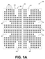
- FIG. 1A-1C an exemplary technique for arranging the electrical contacts of a circuit chip to provide for improved conductive trace routing in the corresponding circuit package is illustrated in accordance with at least one embodiment of the present disclosure.
- Figure 1A illustrates an overhead view of a surface 102 of a circuit chip 104 having a plurality of electrical contacts (e.g., electrical contacts 106) positioned at the surface 102.
- the electrical contacts may be used to conduct signals to and from one or more circuit components (not shown) utilized in the circuit chip 104, as well as to provide power and ground connections to the circuit components.
- the electrical contacts may take many different forms.
- the electrical contacts may be electrically conductive pads having high temperature solder balls (e.g., 0.005 inch in diameter with 95% lead and 5% tin) soldered thereto. These solder balls may then be soldered to corresponding electrical contacts of an underlying circuit package (not shown).
- the electrical contacts may be formed as electrically conductive dendrites, bumps, or studs, which may then be soldered to corresponding electrical contacts of an underlying circuit package (not shown).
- the electrical contacts are positioned or arranged at the surface 102 of the circuit chip 104 so as to form one or more channels substantially absent of electrical contacts.
- the electrical contacts are positioned to form channels 112-130, where the channels 112-126 extend from the periphery of the surface 102 toward the interior of the surface 102 and channels 128 and 130 traverse the surface 102. These channels then may be used to optimize the break out pattern of electrically conductive traces in the corresponding circuit package by routing one or more of the conductive traces from the periphery of the surface 102 to the corresponding electrical contact at least partially via one or more of the channels.
- Figure 1B depicts a top view of an exemplary first routing layer 142 of a circuit package 144 (which may be combined with the circuit chip 104 to form a circuit device 146 as illustrated with reference to Figure 1D).
- the routing layer 142 preferably is positioned substantially parallel to the surface 102 and is substantially coextensive with the surface 102.
- the first routing layer 142 may be in direct contact with the surface 102 of the circuit chip 104 or one or more dielectric or conductive layers may be disposed between the surface 102 and the first routing layer 142.
- the first routing layer 142 may be a top layer of the circuit package 144 or the first routing layer 142 may be an internal layer of the circuit package 144. If the first routing layer 142 is a top layer of the circuit package 144, electrically conductive pads (e.g., pads 148) may be formed at the first routing layer 142 for electrically interconnecting a first subset of the electrical contacts of the circuit chip 104 to the circuit package 144. To provide a conductive path between the electrically conductive pads and the periphery of the circuit package 144, electrically conductive traces (e.g., conductive traces 150) may be formed between the periphery and the respective pads.
- electrically conductive pads e.g., conductive traces 150
- electrically conductive vias may be formed between the first routing layer 142 and a top layer of the circuit package 144 for electrically interconnecting a first subset of the electrical contacts of the circuit chip 104 and the routing layer 142.
- electrically conductive traces e.g., conductive traces 150
- the electrically conductive vias may include, for example, microvias, through holes, and the like.
- channels 112-130 of the circuit chip 104 are substantially devoid of any electrical contacts, it will be appreciated that channels 152-170 corresponding to channels 112-130 thus may be created in the first routing layer 142 as few or no vias are present in these channels 152-170 as no electrical contacts are positioned in the corresponding section of the contact pattern at the surface 102. Accordingly, these channels may be used to facilitate the routing of the electrically conductive traces by routing at least a portion of each of one or more of the electrically conductive traces through one or more of the channels 152-170. The connection of a subset of the electrical contacts of the circuit chip 104 to a routing layer of the circuit package 144 may be repeated for one or more routing layers of the circuit package 144.
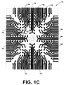
- Figure 1C depicts a top view of an exemplary second routing layer 172 of the circuit package 144.
- the first routing layer 142 is positioned between the second routing layer 172 and the surface 102 and as with the first routing layer 142, the second routing layer 172 preferably is positioned substantially parallel to the surface 102 and is substantially coextensive with the surface 102.
- vias may be formed at the second routing layer 172 to create electrically conductive paths between a second subset of the electrical contacts of the circuit chip 104 and the second routing layer 172.
- electrically conductive traces e.g., conductive traces 176 may be formed between the periphery and the respective vias of the second routing layer 172 to provide conductive paths between these vias and the periphery of the circuit package 144 (and thus conductive paths between the corresponding electrical contacts and the periphery of the circuit package 144).
- channels 182-190 may be present in the second routing layer 172 as no electrical contact is situated in the corresponding section of the contact pattern at the surface 102. Accordingly, the channels 182-200 may be used to facilitate the routing of the electrically conductive traces by routing at least a portion of each of one or more of the electrically conductive traces through one or more of the channels 182-200. This process may be repeated for a third routing layer, a fourth routing layer, and so on.
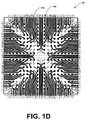
- Figure 1D illustrates an overlay view of the first routing layer 142 and the second routing layer 172.
- the channels formed in the routing layers 142 and 172 resulting from the arrangement of the electrical contacts of the circuit chip 104 may be advantageously used to arrange vias and route conductive traces for the electrical contacts without overcrowding a particular routing layer or requiring an excessive number of routing layers.
- fewer electrical contacts could be broken out for any given routing layer, resulting in the need for more than two routing layers to break out all of the electrical contacts of the circuit chip 104.
- Figure 1E illustrates an expanded view of the circuit device 146 formed from the circuit chip 104 of Figure 1A and the circuit package 144 of Figures 1B and 1C in accordance with an embodiment of the present disclosure.
- Figure 1E shows the pitch of circuit package contacts (e.g., contacts 149) to be 0.100 inches for an exemplary embodiment.
- Figure 1E also shows the pitch of the circuit chip contacts/vias (e.g., contacts/vias 148 and 174) to be 0.012 inches for an exemplary embodiment.
- Figure 1E further shows the size of the circuit chip 104 to be 0.100 x 0.100 square inches for an exemplary embodiment.
- FIG. 2-10 additional exemplary electrical contact arrangements that form one or more channels on a circuit chip that are substantially devoid of electrical contacts are illustrated in accordance with at least one embodiment of the present disclosure.
- various exemplary electrical contact arrangements are depicted for illustrative purposes, those skilled in the art may utilize other contact arrangements using the guidelines provided herein without departing from the spirit or the scope of the present disclosure.
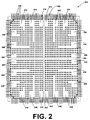
- Figure 2 illustrates an overhead view of a surface 202 of a circuit chip 204 having a plurality of electrical contacts (e.g., contacts 206) arranged so as to form channels 212-264 at the surface 202.
- the electrical contacts may be arranged so as to form channels 212-260 that extend partially from the periphery of the surface 202 to an interior of the surface 202 whereas channels 262 and 264 traverse the surface 202.
- the formation of the channels 212-260 result in a "snowflake" pattern that has the benefit of causing a reduced density of electrical contacts at the peripheral sections of the surface 202, thereby facilitating a more orderly routing of electrically conductive traces at the one or more routing layers of a corresponding circuit package (not shown).
- a "snowflake" pattern that has the benefit of causing a reduced density of electrical contacts at the peripheral sections of the surface 202, thereby facilitating a more orderly routing of electrically conductive traces at the one or more routing layers of a corresponding circuit package (not shown).
- other random patterns that are symmetric or non-symmetric about the center of the surface 202 of the circuit chip 204 may be utilized in accordance with the present disclosure.
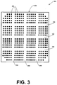
- Figure 3 illustrates an overhead view of a surface 302 of an exemplary circuit chip 304 having electrical contacts (e.g., electrical contacts 306) arranged at the surface 302 so as to form channels 312-322 which traverse the surface 302, resulting in the segmentation of the electrical contacts into sixteen grid sections.
- Figure 4 illustrates an overhead view of a surface 402 of a circuit chip 404 having electrical contacts (e.g., contacts 406) arranged at the surface 402 so as to form channels 412 and 414 which traverse the surface 402 and segment the contacts into four grid sections.
- Figure 5 illustrates an overhead view of a surface 502 of a circuit chip 504 having electrical contacts (e.g., contacts 506) arranged at the surface 502 so as to form channels 508 and 510 extend diagonally across the surface 502 that segment the surface 502 into four roughly triangular sections.
- Figure 6 illustrates an overhead view of a surface 602 of a circuit chip 604 having electrical contacts (e.g., contacts 606) arranged at the surface 602 so as to form diagonal channels 608-618 that segment the surface 602 into twelve roughly triangular or diamond-shaped sections.
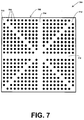
- FIG. 7 depicts an overhead view of a surface 702 of a circuit chip 704 having electrical contacts (e.g., contacts 706) arranged at the surface 702 so as to form diagonal channels 710 and 712 and traverse channels 714 and 716
- Figure 8 depicts an overhead view of a surface 802 of a circuit chip 804 having electrical contacts (e.g., contacts 806) arranged at the surface 802 so as to form diagonal channels 810-816 and traverse channels 818 and 820.
- Figure 9 depicts an overhead view of a surface 902 of a circuit chip 904 having electrical contacts (e.g., contacts 906) arranged at the surface 902 so as to form traverse channels 910 and 912 and traverse channels 714 and 716 and "L" shaped channels 914-920 at the corners of the surface 902.
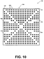
- Figure 10 depicts an overhead view of a surface 1002 of a circuit chip 1004 having electrical contacts (e.g., contacts 1006) arranged at the surface 1002 so as to form diagonal channels 1010 and 1012 and stepped channels 1014-1020.
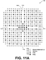
- Figure 11A illustrates an overhead view of a surface 1102 of a circuit chip 1104 having a plurality of electrical contacts positioned at the surface 1102. As noted above, these contacts may be used to conduct signals to and from one or more circuit components (not shown) utilized in the circuit chip 1104 or to provide power and ground connections to the circuit components.
- the electrical contacts are positioned or arranged at the surface 1102 of the circuit chip 1104 so as to form one or more channels substantially absent of electrical contacts.
- the electrical contacts are positioned to form channels 1114-1120, where the channels 1114-1120 extend from the periphery of the surface 1102 toward the interior of the surface 1102, where channels may be used to optimize the break out pattern of electrically conductive traces in the corresponding circuit package by routing one or more of the conductive traces from the periphery of the surface 1102 to the corresponding electrical contacts at least partially via one or more of the channels.
- those electrical contacts that are used to carry high-speed signals may be positioned at or near the periphery of surface 1102 or at or near the sides of the channels 1114-1120, while less critical contacts, such as power contact (e.g., contacts 1108) or ground contacts (e.g., contacts 1110) or low-speed signals (e.g., contacts 1112), may be positioned toward the interior of the surface 1102 or away from the sides of the channels 1114-1120.
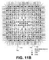
- Figure 11B illustrates an overlay view of the surface 1102 of the circuit chip 1104 and at least first and second routing layers of a chip package corresponding to the circuit chip 1104.
- the lighter-shaded conductive traces e.g., traces 1122 and 1124
- the darker-shaded conductive traces e.g., traces 1126 and 1128
- the channels formed in the routing layers 142 and 172 as a result of, or corresponding to, the arrangement of the electrical contacts of the circuit chip 1104 may be advantageously used to arrange vias and route conductive traces for the electrical contacts without overcrowding a particular routing layer or requiring an excessive number of routing layers.
- the placement of those contacts which carry high-speed signals at or near the periphery of the surface or at or near the side of a channel enables the use of shorter conductive traces to breakout the contacts of the circuit chip 1104 to the exterior of the corresponding chip package, thereby reducing the transmission delays of the high-speed signals over the corresponding conductive traces.
- Figure 12A illustrates an overlay view of a surface of a circuit chip 1204 and at least first routing layer 1208 and second routing layer 1210 of a chip package corresponding to the circuit chip 1204 combined to form a circuit device 1200.
- the lighter-shaded conductive traces (e.g., traces 1222 and 1224) represent conductive traces at the first routing layer 1208 adjacent to the surface of the circuit chip 1204 and the darker-shaded conductive traces (e.g., traces 1226 and 1228) represent conductive traces at the second routine layer 1210.
- Figures 12B and 12C illustrate an overhead view of only the first routing layer 1206 and the second routing layer 1208, respectively, for purposes of clarity.
- the electrical contacts are positioned at the surface of the circuit chip 1202 such that the peripheral portion of the surface of the circuit chip has a higher density of electrical contacts than the interior portion, where the inner portion preferably is substantially devoid of electrical contacts.
- the different densities of electrical contacts may be accomplished by utilizing a larger die for the circuit chip than conventionally would be used for the same number of electrical contacts and positioning the electrical contacts toward the periphery of the larger-size die. As a result, the electrical contacts may be more spaciously distributed, thereby allowing for a more effective conductive trace routing pattern to breakout the electrical contacts.
- one or more thermal conductors 1230, or thermal input/outputs (I/Os) may be positioned at the interior portion of the surface of the circuit chip 1204 to conduct heat away from the circuit chip 1204.
Landscapes
- Engineering & Computer Science (AREA)
- Microelectronics & Electronic Packaging (AREA)
- Semiconductor Integrated Circuits (AREA)
- Internal Circuitry In Semiconductor Integrated Circuit Devices (AREA)
- Wire Bonding (AREA)
Abstract
Description
Claims (18)
- A circuit device comprising:a circuit chip having a plurality of electrical contacts positioned at a surface of the circuit chip so as to form one or more channels at the surface of the circuit chip, the one or more channels being substantially devoid of electrical contacts such that one or more corresponding channels are formed in a chip carrier for routing electrically conductive traces from one or more of the plurality of electrical contacts on a routing layer of the chip carrier.
- The circuit device as in Claim 1, further comprising:a chip carrier having at least one routing layer for routing electrically conductive traces from one or more of the plurality of electrical contacts toward a periphery of the chip carrier, wherein one or more conductive traces are routed via one or more channels in the at least one routing layer substantially corresponding to one or more of the plurality of channels at the surface of the circuit chip.
- The circuit device as in Claim 2, wherein the one or more channels in the at least one routing layer are substantially devoid of vias.
- The circuit device as in Claim 1, wherein the plurality of electrical contacts include a plurality of signal contacts and a plurality of power and ground contacts, wherein one or more of the plurality of signal contacts are positioned at a periphery of the surface of the circuit chip and one or more of the plurality of power and ground contacts are positioned at an interior of the surface of the circuit chip.
- The circuit device as in Claim 4, wherein one or more of the plurality of signal contacts are positioned adjacent to at least one of the one or more channels.
- The circuit device as in Claim 1, wherein at least one of the one or more channels extend from a periphery of the surface of the circuit chip into an interior of the surface of the circuit chip.
- A circuit device comprising:wherein a substantial portion of the plurality of power and ground electrical contacts are positioned at an interior of the surface of the circuit chip; anda circuit chip having a plurality of power and ground electrical contacts and a plurality of signal electrical contacts positioned at a surface of the circuit chip;
wherein a substantial portion of the plurality of signal electrical contacts are positioned at a periphery of the surface of the circuit chip. - The circuit device as in Claim 7, wherein the plurality of power and ground electrical contacts and the plurality of signal electrical contacts are positioned so as to form one or more channels at the surface of the circuit chip, the one or more channels being substantially devoid of electrical contacts such that one or more corresponding channels are formed in a chip carrier for routing electrically conductive traces from one or more of the plurality of electrical contacts on a routing layer of the chip carrier.
- The circuit device as in Claim 8, further comprising:wherein one or more conductive traces are routed via one or more channels in the at least one routing layer substantially corresponding to one or more of the plurality of channels at the surface of the circuit chip.a chip carrier having at least one routing layer for routing electrically conductive traces from one or more of the electrical contacts toward a periphery of the chip carrier,
- The circuit device as in Claim 8, wherein a substantial portion of the plurality of signal electrical contacts are positioned adjacent to at least one of the one or more channels.
- A circuit device comprising:wherein a peripheral portion of the surface of the circuit chip has a first density of electrical contacts;a circuit chip having a plurality of electrical contacts positioned at a surface of the circuit chip;
wherein an interior portion of the surface of the circuit chip has a second density of electrical contacts; and
wherein the second density is substantially less than the first density. - The circuit device as in Claim 11, wherein the circuit chip further comprises at least one thermal transfer contact positioned at the interior portion of the surface of the circuit chip.
- The circuit device as in Claim 11, wherein the plurality of electrical contacts are positioned so as to form one or more channels at the surface of the circuit chip, the one or more channels being substantially devoid of electrical contacts such that one or more corresponding channels are formed in a chip carrier for routing electrically conductive traces from one or more of the plurality of electrical contacts on a routing layer of the chip carrier.
- The circuit device as in Claim 13, further comprising:a chip carrier having at least one routing layer for routing electrically conductive traces from one or more of the plurality of electrical contacts toward a periphery of the chip carrier, wherein one or more conductive traces are routed via one or more channels in the at least one routing layer substantially corresponding to one or more of the plurality of channels at the surface of the circuit chip.
- A method comprising:positioning a plurality of electrical contacts at a surface of a circuit chip so as to form one or more channels at the surface of the circuit chip, the one or more channels being substantially clear of electrical contacts; andforming one or more electrically conductive traces at one or more routing layers of a chip carrier supporting the circuit chip, wherein the one or more electrically conductive traces are routed from one or more of the plurality of electrical contacts toward a periphery of the chip carrier via one or more channels in the at least one routing layer substantially corresponding to one or more of the plurality of channels at the surface of the circuit chip.
- The method as in Claim 15, wherein the one or more channels in the at least one routing layer of the chip carrier are substantially devoid of vias.
- The method as in Claim 15, wherein the plurality of electrical contacts include a plurality of signal contacts and a plurality of power and ground contacts, and wherein one or more of the plurality of signal contacts are positioned at a periphery of the surface of the circuit chip and one or more of the plurality of power and ground contacts are positioned at an interior of the surface of the circuit chip.
- The method as in Claim 17, wherein one or more of the plurality of signal contacts are positioned adjacent to at least one of the one or more channels.
Applications Claiming Priority (4)
| Application Number | Priority Date | Filing Date | Title |
|---|---|---|---|
| US50109403P | 2003-09-09 | 2003-09-09 | |
| US501094P | 2003-09-09 | ||
| US848044 | 2004-05-19 | ||
| US10/848,044 US20040212103A1 (en) | 2000-06-19 | 2004-05-19 | Techniques for pin arrangements in circuit chips |
Publications (2)
| Publication Number | Publication Date |
|---|---|
| EP1515366A2 true EP1515366A2 (en) | 2005-03-16 |
| EP1515366A3 EP1515366A3 (en) | 2007-03-21 |
Family
ID=34139063
Family Applications (1)
| Application Number | Title | Priority Date | Filing Date |
|---|---|---|---|
| EP04394053A Withdrawn EP1515366A3 (en) | 2003-09-09 | 2004-08-20 | Techniques for pad arrangements on circuit chips |
Country Status (3)
| Country | Link |
|---|---|
| US (1) | US20040212103A1 (en) |
| EP (1) | EP1515366A3 (en) |
| CA (1) | CA2478906A1 (en) |
Cited By (1)
| Publication number | Priority date | Publication date | Assignee | Title |
|---|---|---|---|---|
| EP1753274A3 (en) * | 2005-08-10 | 2009-01-14 | Alcatel Lucent | Alternating micro-vias and through-hole vias for a BGA interconnect grid in order to create improved PCB routing channels |
Families Citing this family (10)
| Publication number | Priority date | Publication date | Assignee | Title |
|---|---|---|---|---|
| US7725860B1 (en) * | 2000-06-19 | 2010-05-25 | Herman Kwong | Contact mapping using channel routing |
| US7345245B2 (en) * | 2003-10-08 | 2008-03-18 | Lsi Logic Corporation | Robust high density substrate design for thermal cycling reliability |
| US20060185895A1 (en) * | 2005-02-24 | 2006-08-24 | Navinchandra Kalidas | Universal pattern of contact pads for semiconductor reflow interconnections |
| US7343577B2 (en) * | 2005-09-13 | 2008-03-11 | Alcatel | Area array routing masks for improved escape of devices on PCB |
| WO2008058258A2 (en) * | 2006-11-08 | 2008-05-15 | Mentor Graphics Corporation | Use of breakouts in printed circuit board designs |
| US20080185181A1 (en) * | 2006-11-08 | 2008-08-07 | Pfeil Charles L | Alternating via fanout patterns |
| US8093708B2 (en) * | 2009-07-06 | 2012-01-10 | Sony Ericsson Mobile Communications Ab | Semiconductor package having non-uniform contact arrangement |
| US9345137B2 (en) | 2013-11-04 | 2016-05-17 | Lattice Semiconductor Corporation | Partially depopulated interconnection arrays for packaged semiconductor devices and printed circuit boards |
| CN105574237B (en) * | 2015-12-10 | 2018-12-21 | 广东顺德中山大学卡内基梅隆大学国际联合研究院 | System in package BGA power ground pin distribution optimization method based on population |
| CN105608257B (en) * | 2015-12-15 | 2018-12-21 | 广东顺德中山大学卡内基梅隆大学国际联合研究院 | The optimal pin of extensive BGA package based on genetic algorithm is distributed generation method |
Family Cites Families (31)
| Publication number | Priority date | Publication date | Assignee | Title |
|---|---|---|---|---|
| US5006820A (en) * | 1989-07-03 | 1991-04-09 | Motorola, Inc. | Low reflection input configuration for integrated circuit packages |
| JP2739726B2 (en) * | 1990-09-27 | 1998-04-15 | インターナシヨナル・ビジネス・マシーンズ・コーポレーシヨン | Multilayer printed circuit board |
| JP2966972B2 (en) * | 1991-07-05 | 1999-10-25 | 株式会社日立製作所 | Semiconductor chip carrier, module mounting the same, and electronic device incorporating the same |
| US5544018A (en) * | 1994-04-13 | 1996-08-06 | Microelectronics And Computer Technology Corporation | Electrical interconnect device with customizeable surface layer and interwoven signal lines |
| JP2679681B2 (en) * | 1995-04-28 | 1997-11-19 | 日本電気株式会社 | Semiconductor device, package for semiconductor device, and manufacturing method thereof |
| US5784262A (en) * | 1995-11-06 | 1998-07-21 | Symbios, Inc. | Arrangement of pads and through-holes for semiconductor packages |
| US5686764A (en) * | 1996-03-20 | 1997-11-11 | Lsi Logic Corporation | Flip chip package with reduced number of package layers |
| US5847936A (en) * | 1997-06-20 | 1998-12-08 | Sun Microsystems, Inc. | Optimized routing scheme for an integrated circuit/printed circuit board |
| US5942795A (en) * | 1997-07-03 | 1999-08-24 | National Semiconductor Corporation | Leaded substrate carrier for integrated circuit device and leaded substrate carrier device assembly |
| JP3466443B2 (en) * | 1997-11-19 | 2003-11-10 | 新光電気工業株式会社 | Multilayer circuit board |
| JP3380151B2 (en) * | 1997-12-22 | 2003-02-24 | 新光電気工業株式会社 | Multilayer circuit board |
| US6294407B1 (en) * | 1998-05-06 | 2001-09-25 | Virtual Integration, Inc. | Microelectronic packages including thin film decal and dielectric adhesive layer having conductive vias therein, and methods of fabricating the same |
| US6232564B1 (en) * | 1998-10-09 | 2001-05-15 | International Business Machines Corporation | Printed wiring board wireability enhancement |
| US6057596A (en) * | 1998-10-19 | 2000-05-02 | Silicon Integrated Systems Corp. | Chip carrier having a specific power join distribution structure |
| JP2000174153A (en) * | 1998-12-01 | 2000-06-23 | Shinko Electric Ind Co Ltd | Multilayer wiring board |
| US6310398B1 (en) * | 1998-12-03 | 2001-10-30 | Walter M. Katz | Routable high-density interfaces for integrated circuit devices |
| US6181004B1 (en) * | 1999-01-22 | 2001-01-30 | Jerry D. Koontz | Digital signal processing assembly and test method |
| US6246121B1 (en) * | 1999-04-12 | 2001-06-12 | Vlsi Technology, Inc. | High performance flip-chip semiconductor device |
| US6198635B1 (en) * | 1999-05-18 | 2001-03-06 | Vsli Technology, Inc. | Interconnect layout pattern for integrated circuit packages and the like |
| US6037677A (en) * | 1999-05-28 | 2000-03-14 | International Business Machines Corporation | Dual-pitch perimeter flip-chip footprint for high integration asics |
| US6664620B2 (en) * | 1999-06-29 | 2003-12-16 | Intel Corporation | Integrated circuit die and/or package having a variable pitch contact array for maximization of number of signal lines per routing layer |
| US6150729A (en) * | 1999-07-01 | 2000-11-21 | Lsi Logic Corporation | Routing density enhancement for semiconductor BGA packages and printed wiring boards |
| JP3562568B2 (en) * | 1999-07-16 | 2004-09-08 | 日本電気株式会社 | Multilayer wiring board |
| JP2001053437A (en) * | 1999-08-06 | 2001-02-23 | Shinko Electric Ind Co Ltd | Multilayer circuit board |
| US6256769B1 (en) * | 1999-09-30 | 2001-07-03 | Unisys Corporation | Printed circuit board routing techniques |
| US6373139B1 (en) * | 1999-10-06 | 2002-04-16 | Motorola, Inc. | Layout for a ball grid array |
| US6454876B1 (en) * | 1999-12-22 | 2002-09-24 | The Clorox Company | Method for eliminating malodors |
| US6388890B1 (en) * | 2000-06-19 | 2002-05-14 | Nortel Networks Limited | Technique for reducing the number of layers in a multilayer circuit board |
| US6762366B1 (en) * | 2001-04-27 | 2004-07-13 | Lsi Logic Corporation | Ball assignment for ball grid array package |
| US20030043560A1 (en) * | 2001-06-15 | 2003-03-06 | Clarkson Robert Roy | Printed circuit board having a microelectronic semiconductor device mount area for trace routing therethrough |
| US6521846B1 (en) * | 2002-01-07 | 2003-02-18 | Sun Microsystems, Inc. | Method for assigning power and ground pins in array packages to enhance next level routing |
-
2004
- 2004-05-19 US US10/848,044 patent/US20040212103A1/en not_active Abandoned
- 2004-08-20 EP EP04394053A patent/EP1515366A3/en not_active Withdrawn
- 2004-08-24 CA CA002478906A patent/CA2478906A1/en not_active Abandoned
Cited By (2)
| Publication number | Priority date | Publication date | Assignee | Title |
|---|---|---|---|---|
| EP1753274A3 (en) * | 2005-08-10 | 2009-01-14 | Alcatel Lucent | Alternating micro-vias and through-hole vias for a BGA interconnect grid in order to create improved PCB routing channels |
| US7714234B2 (en) | 2005-08-10 | 2010-05-11 | Alcatel Lucent | Alternating micro-vias and throughboard vias to create PCB routing channels in BGA interconnect grid |
Also Published As
| Publication number | Publication date |
|---|---|
| CA2478906A1 (en) | 2005-03-09 |
| US20040212103A1 (en) | 2004-10-28 |
| EP1515366A3 (en) | 2007-03-21 |
Similar Documents
| Publication | Publication Date | Title |
|---|---|---|
| US6344616B1 (en) | Cable capable of connecting between integrated circuit elements in a reduced space | |
| US6472293B2 (en) | Method for manufacturing an interconnect structure for stacked semiconductor device | |
| US7863526B2 (en) | High performance chip carrier substrate | |
| US6545876B1 (en) | Technique for reducing the number of layers in a multilayer circuit board | |
| US8581392B2 (en) | Silicon based microchannel cooling and electrical package | |
| EP1347674A2 (en) | Technique for reducing the number of layers in a multilayer circuit board | |
| KR20010062054A (en) | Semiconductor device | |
| EP1515366A2 (en) | Techniques for pad arrangements on circuit chips | |
| US6882046B2 (en) | Single package containing multiple integrated circuit devices | |
| US6664620B2 (en) | Integrated circuit die and/or package having a variable pitch contact array for maximization of number of signal lines per routing layer | |
| US7069650B2 (en) | Method for reducing the number of layers in a multilayer signal routing device | |
| JP2020520559A (en) | Low crosstalk vertical connection interface | |
| US7259336B2 (en) | Technique for improving power and ground flooding | |
| US6774498B2 (en) | Flip-chip package substrate | |
| CN216902914U (en) | Silicon-based substrate and chip | |
| US20250380355A1 (en) | Wiring substrate | |
| US20020113307A1 (en) | High-density flip-chip interconnect | |
| US20250096097A1 (en) | Semiconductor package and method for manufacturing same | |
| CN115279014B (en) | A printed circuit board structure and a method for manufacturing the same | |
| Chen et al. | An overview of electrical and mechanical aspects of electronic packaging | |
| US20030085455A1 (en) | Thermal ring used in 3-D stacking | |
| Martinez et al. | The TCC/MCM:/spl mu/BGA on a laminated substrate | |
| CN118448384A (en) | Bearing substrate |
Legal Events
| Date | Code | Title | Description |
|---|---|---|---|
| PUAI | Public reference made under article 153(3) epc to a published international application that has entered the european phase |
Free format text: ORIGINAL CODE: 0009012 |
|
| AK | Designated contracting states |
Kind code of ref document: A2 Designated state(s): AT BE BG CH CY CZ DE DK EE ES FI FR GB GR HU IE IT LI LU MC NL PL PT RO SE SI SK TR |
|
| AX | Request for extension of the european patent |
Extension state: AL HR LT LV MK |
|
| PUAL | Search report despatched |
Free format text: ORIGINAL CODE: 0009013 |
|
| AK | Designated contracting states |
Kind code of ref document: A3 Designated state(s): AT BE BG CH CY CZ DE DK EE ES FI FR GB GR HU IE IT LI LU MC NL PL PT RO SE SI SK TR |
|
| AX | Request for extension of the european patent |
Extension state: AL HR LT LV MK |
|
| AKX | Designation fees paid | ||
| REG | Reference to a national code |
Ref country code: DE Ref legal event code: 8566 |
|
| STAA | Information on the status of an ep patent application or granted ep patent |
Free format text: STATUS: THE APPLICATION IS DEEMED TO BE WITHDRAWN |
|
| 18D | Application deemed to be withdrawn |
Effective date: 20070922 |