【0001】
【発明の属する技術分野】
本発明は、スパッタリングにより膜の応力が緩和された金属酸化物膜の単層膜、金属酸化物膜と二酸化ケイ素膜との多層膜付き基板、およびそれらの膜付き基板の製造方法に関するものである。
【0002】
【従来の技術】
金属酸化物薄膜の光学的応用は、単層の熱線反射ガラスや反射防止膜から始まり、さらに特定の波長の光が選択的に反射または透過するように設計した多層膜系の反射防止コート、反射増加コート、干渉フィルタ、偏光膜など多分野にわたっている。多層膜の分光特性は、各層の屈折率nと膜厚をパラメータとして光学的設計され、一般的に高屈折率膜と低屈折率膜とを組合わせて調整される。優れた光学特性を実現するには、高屈折率膜と低屈折率膜との屈折率nの差が大きい方がよく、例えば、n=2.4の二酸化チタン、n=2.3の五酸化ニオブ、n=2.1の五酸化タンタル、またはn=2.0の三酸化タングステンと、n=1.38のフッ化マグネシウムまたはn=1.46の二酸化ケイ素との組合わせが好適である。これら単層膜や多層膜は、真空蒸着法、塗布法等で成膜できる。
【0003】
一方、建築用ガラスや自動車用ガラス、CRTやフラットディスプレイ等の大面積基板に、単層膜または多層膜を成膜する場合には、スパッタリング法、特に直流(DC)スパッタリング法が用いられることが多い。
ところで、高屈折率膜をDCスパッタリング法で成膜する場合は、導電性を有する金属質ターゲットを用い、酸素を含む雰囲気でスパッタリングする、いわゆる反応性スパッタリングによるのが現状である。しかし、この方法で得られる薄膜の成膜速度は極めて遅く、生産性が悪く、コストが高くなるという問題があった。
【0004】
これを回避するために、高いスパッタリング電力を投入することが考えられるが、ターゲット材の冷却が追いつかない場合には、割れ、剥離等のトラブルが起きる可能性が高くなるため、投入できる電力には限界があった。加えて、得られた金属酸化物膜の応力が高いため、膜付き基板の反りの原因となることがあった。特に金属酸化物膜と二酸化ケイ素膜とが交互に何層も積層してなる多層膜を板厚の薄い基板に設けた場合には、合計膜厚の増加に伴って反りが大きくなる傾向があったので、最終的に必要な板厚以上の厚い基板に成膜して反りを防ぎ、所望の大きさに切断した後、基板を研磨して必要な厚みとするなどの対策をとっていた。
【0005】
また、化学量論的組成より酸素が不足している金属酸化物MOx (ただし、MはTi、Nb、Ta、Mo、W、ZrおよびHfからなる群から選ばれる少なくとも1種の金属を示す)をターゲット材に用いて、DCスパッタリングを行い高屈折率を有する透明金属酸化物膜を透明基板上に成膜する方法も提案されている(例えば、特許文献1参照。)。しかし、この公報には、膜の反りや応力について一切記載されていない。
【0006】
【特許文献1】
国際公開番号(再公表特許)97/08359号公報
【0007】
【発明が解決しようとする課題】
本発明は、導電性スパッタリング材を用いて、スパッタリング法により、金属酸化物膜と二酸化ケイ素膜との多層膜を基板の上に高速成膜して、膜の応力が緩和された、すなわち低応力の多層膜付き基板とそのような低応力の多層膜付き基板を製造する方法を提供することが目的である。基板の反りが少ない膜付き基板を得るためには、金属酸化物膜と二酸化ケイ素膜とが積層された多層膜付き基板の応力は、−100MPa 〜+100MPa であることが必要であり、好ましくは−60MPa 〜+60MPa であり、特に好ましくは−30MPa 〜+30MPa である。なお、応力がプラス(+)側にあるときは引張応力であり、マイナス(−)側にあるときは圧縮応力である。
【0008】
【課題を解決するための手段】
本発明は、基板上に、少なくとも金属酸化物膜と二酸化ケイ素膜とを1回以上繰返し積層して成膜されてなる多層膜付き基板であって、該金属酸化物膜の少なくとも1層が化学量論的組成より酸素が不足している金属酸化物MOx (ただし、MはTi、Nb、Ta、Mo、W、ZrおよびHfからなる群から選ばれる少なくとも1種の金属を示す)をターゲット材に用いてスパッタリングを行うことにより成膜されてなる酸素不足が解消された金属酸化物膜であり、かつ該多層膜の応力が−100MPa 〜+100MPa であることを特徴とする多層膜付き基板である。
【0009】
本発明の多層膜付き基板は、金属酸化物MOx の金属Mが、Nbおよび/またはTaの場合には、Xが2<X<2.5であることが好ましい。
【0010】
また、本発明の多層膜付き基板は、金属酸化物MOx の金属MがTi、ZrおよびHfからなる群から選ばれる少なくとも1種の金属の場合には、Xが1<X<2であることが好ましい。
【0011】
また、本発明の多層膜付き基板は、金属酸化物MOx の金属MがMoおよび/またはWの場合には、Xが2<X<3であることが好ましい。
【0012】
また、本発明の多層膜付き基板は、該多層膜の応力が−60MPa 〜+60MPa であることが好ましい。
【0013】
また、本発明の多層膜付き基板は、前記金属酸化物膜と二酸化ケイ素膜を10回以上繰返し積層してなることが好ましい。
【0014】
本発明は、少なくとも金属酸化物膜と二酸化ケイ素膜とが交互に積層されてなる多層膜付き基板の製造方法であって、該金属酸化物膜の少なくとも一層が化学量論的組成より酸素が不足している金属酸化物MOx (ただし、MはTi、Nb、Ta、Mo、W、ZrおよびHfからなる群から選ばれる少なくとも1種の金属を示す)をターゲット材に用いてスパッタリングを行うことにより成膜され、かつ該多層膜の応力が−100MPa 〜+100MPa であることを特徴とする多層膜付き基板の製造方法である。
【0015】
【発明の実施の形態】
本発明の多層膜付き基板は、化学量論的組成より酸素が不足している金属酸化物MOx をターゲット材に用いて、スパッタリングを行い、基板上に酸素不足が解消された金属酸化物膜を成膜する方法により製造される。
本発明で金属酸化物膜を得るために使用されるターゲット材は金属酸化物であって、化学量論的組成より酸素が不足している金属酸化物MOx (ただし、MはTi、Nb、Ta、Mo、W、ZrおよびHfからなる群から選ばれる少なくとも1種の金属を示す)であり、2種以上の金属Mを含んでいてもよい。
【0016】
MがNbおよび/またはTaの場合には、Xが2<X<2.5であるのが好ましい。これは、Xが2.5の場合は、Nbおよび/またはTaが完全に酸化している状態なので、ターゲット材は電気絶縁性であり、DCスパッタリングができないためである。また、Xが2以下では、NbOx および/またはTaOx が化学的に不安定であり、ターゲット材としては好ましくない。NbOx を用いた場合には、高い成膜速度を実現でき、TaOx を用いた場合には、高い耐食性と高い耐擦傷性を有する膜を成膜できる。
【0017】
前記と同様な理由から、本発明のターゲット材のMOx のMがMoおよび/またはWである場合には、Xが2<X<3であるのが好ましい。
【0018】
また本発明のターゲット材のMOx のMがTi、ZrおよびHfからなる群から選ばれる少なくとも1種の金属である場合には、Xが1<X<2であるのが好ましい。
【0019】
本発明で金属酸化物膜を得るために使用されるターゲット材には、金属酸化物MOx による膜の応力を緩和することを含む特性を損なわない限り、金属酸化物MOx を構成する金属M以外の金属の酸化物を添加して、屈折率や機械的、化学的特性などの膜の性能を向上させることができる。このような金属酸化物としては、Cr、Ce、Y、Si、AlおよびBからなる群から選ばれる少なくとも1種の金属の酸化物が挙げられる。これらは酸素欠損型である必要はない。例えば、Crの酸化物の場合は、膜の耐食性が改善され、Ceの酸化物の場合は、金属酸化物膜に紫外線カット性を付与することができる。
【0020】
本発明で金属酸化物膜を得るために使用されるターゲット材は、例えばNbOx (ただし、2<X<2.5)の場合には、次のようにして製造される。他の金属酸化物の場合も本質的に変わるところはない。
Nb2 O5 粉末を非酸化雰囲気でホットプレス(高温高圧プレス)して焼結することにより、化学量論的組成より酸素が不足している(酸素が欠損した)NbOx (ただし、2<X<2.5)を製造する。Nb2 O5 粉末の粒径は0.05〜40μmが適当である。ホットプレスの雰囲気は非酸化性雰囲気とすることが重要であり、ターゲット材の酸素含有量の調整が容易なことから、アルゴンや窒素が好ましい。また、水素を添加することもできる。ホットプレスの条件は、特に制限されないが、温度は800〜1400℃が好ましく、圧力は4.90×10⁶ 〜9.80×10⁶Pa が好ましい。
NbOx 焼結体の密度は4.0〜4.4g/cm3 程度、比抵抗は0.1〜0.3Ωcm程度である。
また、TiOx 焼結体の密度は3.8〜4.2g/cm3 程度、比抵抗は0.1〜0.4Ωcm程度である。
【0021】
また、基板上に、金属または合金からなるアンダーコートを施し、アンダーコート上に、金属酸化物を還元雰囲気下の高温プラズマガス中で、半溶融状態にしつつ、このガスにより半溶融物をアンダーコート上に輸送して付着させるプラズマ溶射により、金属酸化物を形成することによっても、化学量論的組成より酸素が不足している金属酸化物からなる本発明に使用されるターゲット材を得ることができる。
【0022】
本発明において、金属酸化物膜が成膜される基板は、ガラス、樹脂フィルム、シリコンなどであり、特に限定されない。
【0023】
本発明の膜の応力が緩和された金属酸化物膜を含む多層膜付き基板は、例えば下記の方法により製造されるが、これに限定されるものではない。
【0024】
本発明で金属酸化物膜を得るために使用されるターゲット材は、金属酸化物で構成されており、かつ、化学量論的組成より少しだけ酸素不足状態になっている。したがって、金属酸化物膜の成膜を行う場合には、スパッタリングの雰囲気から、化学量論的組成より少しだけ不足している酸素を補えば、酸素不足が解消された金属酸化物膜が得られる。
【0025】
例えば、化学量論的組成より少しだけ酸素不足状態になっている金属酸化物をターゲット材に用いて、アルゴン雰囲気中またはアルゴンと少量の酸素との混合雰囲気中で、圧力を0.15〜1.5Pa程度としてDCスパッタリングすると、基板上に均一な透明膜、すなわち酸素不足が解消された金属酸化物膜を高速で成膜することができる。金属ターゲットを用いる場合には、酸素分圧の変化によって、成膜速度や放電電流・電圧の不連続な変化であるヒステリシス現象が生じるが、該金属酸化物をターゲット材に用いた場合には、このようなヒステリシス現象は生じず、成膜時の成膜速度の制御が比較的容易であり、しかも、供給する酸素ガス量を必要最低限、あるいはそれに近い量まで少なくすることができる。
【0026】
酸素の割合が小さくなると、金属酸化物膜が金属膜に近くなり吸収膜になる傾向がある。逆に、酸素の割合が大きくなると成膜速度が低下し、金属酸化物膜の応力が大きな圧縮応力になる傾向が現れる。よって、酸素の分圧の調整が重要であり、スパッタリングガス中に酸素が0〜30体積%含まれていることが好ましい。ただし、NbOx を用いたターゲット材においては、スパッタリングガス中に酸素が1〜30体積%含まれていることが好ましい。また金属ターゲット材を用いた場合は、投入電力にも左右されるが、スパッタリングガス中に酸素が30体積%以上含まれていることが吸収膜とならないようにする点で好ましい。
【0027】
成膜される金属酸化物膜の膜厚はスパッタリング時間、投入電力などにより調整されるが、金属酸化物膜の1層の膜厚は10〜1000nm、特に10〜300nmであるのが好ましい。
酸素が不足している金属酸化物ターゲットから成膜される金属酸化物膜は、通常の金属ターゲットから成膜される金属酸化物膜と比較して屈折率などの光学特性は同等にもかかわらず、応力が緩和された膜となっている。この理由は明らかではないが、成膜中の膜の成長過程が異なるためと推測される。
【0028】
次に、前記金属酸化物膜が成膜された、膜付き基板の上に、さらにケイ素をターゲット材に用い、前記金属酸化物をターゲット材に用いた場合と同様にスパッタリングを行い、透明な二酸化ケイ素膜を成膜する。最外層は、金属酸化物膜であっても、二酸化ケイ素膜であってもよい。また、最内層も、金属酸化物膜であっても、二酸化ケイ素膜であってもよい。さらに、前記多層膜が様々な特性に対応できるように、金属酸化物膜と二酸化ケイ素膜以外に両者と異なる第三の膜を介在させることができる。例えば、光学的条件を満足させるために、中程度の屈折率の酸化アルミニウム膜を介在させてもよい。
【0029】
金属酸化物膜と二酸化ケイ素膜とを1回以上5回、10回または50回等の複数回繰返し積層して、100層を超えるような多層膜を成膜することもできる。したがって、多層膜の膜厚は、層の数だけ厚くなるが、金属酸化物膜の応力が二酸化ケイ素膜の応力をある程度打ち消すため、多層膜になっても、反りは極めて小さい。これは、多層膜を製造するに際し、反りを抑制するために、基板の板厚を格別厚くする必要がないことを意味し、成膜後の多層膜付き基板の研磨工程の省略または軽減、多層膜の層数の増加、コストダウンに大きく寄与する。多層膜付き基板の金属酸化物膜の1層の膜厚は10〜1000nm、特に10〜300nmであるのが好ましく、二酸化ケイ素膜の1層の膜厚は10〜1000nm、特に10〜300nmであるのが好ましい。
【0030】
以上は、基板に、初めに金属酸化物膜を成膜し、ついで二酸化ケイ素膜を成膜し、二酸化ケイ素膜が最外層になるような層構成とする場合について説明したが、基板に、初めに二酸化ケイ素膜を成膜し、ついで金属酸化物膜を成膜する場合も、各層の成膜に変わるところがないので、説明を省略する。なお例えば、金属酸化物膜、二酸化ケイ素膜および金属酸化物膜からなる3層膜や、該3層膜にさらに二酸化ケイ素膜と金属酸化物膜を積層してなる5層膜も、便宜的に1回以上繰返し積層してなる本願発明の多層膜付き基板に含める。
【0031】
かくして得られた金属酸化物膜の多層膜付き基板は、各種用途に使用される。以上DCスパッタリングによる多層膜付き基板の成膜について説明したが、交流(AC)スパッタリングによる多層膜付き基板の成膜の場合も同様に実施される。
【0032】
【実施例】
以下、本発明を実施例により説明するが、もちろん本発明はこれら実施例に限定されるものではない。
【0033】
(製造例1)
(NbOx 焼結体)
市販の高純度Nb2 O5 粉末を、カーボン製のホットプレス用金型に充填し、アルゴン雰囲気中で、1100℃に1時間保持した後、圧力4.903×10⁶Pa でホットプレスを行い、焼結体を得た。焼結体の密度および比抵抗を測定した。
次に、焼結体をメノウ乳鉢で粉砕し、空気中で1100℃に加熱し、加熱前後の焼結体の質量を測定した。この加熱により、先の焼結により酸素が不足した状態のNbOx から完全に酸化された焼結体Nb2 O5 に変化したものと推定して、その質量増加分から、焼結体の酸素含有量を計算し,酸素不足を確認した。
焼結体の密度は4.00g/cm3 、比抵抗は0.30Ωcmおよび酸素含有量はNbOx のXとして2.498であった。
【0034】
(製造例2)
(TiOx 焼結体)
製造例1の高純度Nb2 O5 粉末の代わりに、市販の高純度TiO2 粉末を用いる以外は、製造例1と同様の方法・条件で焼結体を得て、焼結体の密度、比抵抗を測定した。
次に、製造例1と同様の方法・条件で加熱し、加熱前後の焼結体の質量を測定し、その質量増加分から、焼結体の酸素含有量を計算し,酸素不足を確認した。焼結体の密度は3.90g/cm3 、比抵抗は0.35Ωcmおよび酸素含有量はTiOx のXとして1.980であった。
【0035】
(参考例1〜6)
製造例1により製造されたNbOx 焼結体を、200mm×70mm、厚さ5mmの直方体に研削加工し、ターゲット材を製造した。このターゲット材を、銅製のパッキングプレートにメタルボンドで接着し、マグネトロンDCスパッタリング装置に取り付けた。1.1mm厚のガラス基板および0.525mm厚で直径10cmのシリコン基板のそれぞれに、投入電力をDC0.75kW、背圧を1×10⁻³Pa、スパッタリング圧力を0.6Paとし、雰囲気中の酸素ガスとアルゴンガスとの総量に対する酸素ガスの割合を表1に示すように調整してスパッタリングを行い、表1に示す膜厚のNb2 O5 膜の成膜を行った。スパッタリング中の放電は極めて安定しており、DCスパッタリングでも安定して成膜することができた。
【0036】
成膜後、膜厚を触針式の膜厚測定装置を用いて測定した。
膜の応力は、Tencor Instruments社のFLX THIN FILMS STRESS MEASUREMENT SYSTEMであるFleXus F2320を使用して、成膜前および成膜後の直径10cmのシリコン基板の反り(曲率半径)を測定することにより求めた。
ガラス基板上の膜の屈折率を、J.A.Woollam Co., Inc. の分光エリプソメータWVASE32 で測定した。なお、膜は透明で膜の光吸収はなかった。
表1に、膜厚、成膜速度、膜の応力、波長550nmにおける膜の屈折率を示した。
【0037】
(参考例7〜11)
参考例1のNbOx ターゲット材の代わりに、市販のNb金属をターゲット材に用い、雰囲気中の酸素ガスとアルゴンガスとの総量に対する酸素ガスの割合を表1に示すように調整する以外は参考例1と同様に、スパッタリングを行い、Nb2 O5 膜の成膜を行った。スパッタリング中の放電は極めて安定しており、DCスパッタリングでも安定して成膜することができた。Nb2 O5 膜の特性を参考例1と同様に測定し、その結果を表1に示した。
【0038】
(参考例12〜14)
製造例2により製造されたTiOx 焼結体を、200mm×70mm、厚さ5mmの直方体に研削加工し、ターゲット材を製造した。このターゲット材を、銅製のパッキングプレートにメタルボンドで接着し、マグネトロンDCスパッタリング装置に取り付けた。1.1mm厚のガラス基板および0.525mm厚で直径10cmのシリコン基板のそれぞれに、投入電力をDC0.75kW、背圧を1×10⁻³Pa、スパッタリング圧力を0.6Paとし、雰囲気中の酸素ガスとアルゴンガスとの総量に対する酸素ガスの割合を表1に示すように調整してスパッタリングを行い、表1に示す膜厚のTiO2 膜の成膜を行った。スパッタリング中の放電は極めて安定しており、DCスパッタリングでも安定して成膜することができた。
【0039】
(参考例15〜16)
参考例12のTiOx ターゲット材の代わりに、市販のTi金属をターゲット材に用い、雰囲気中の酸素ガスとアルゴンガスとの総量に対する酸素ガスの割合を表1に示すように調整する以外は参考例12と同様に、スパッタリングを行い、TiO2 膜の成膜を行った。スパッタリング中の放電は極めて安定しており、DCスパッタリングでも安定して成膜することができた。TiO2 膜の特性を参考例1と同様に測定し、その結果を表1に示した。
【0040】
(参考例17〜18)
参考例1のNbOx ターゲット材の代わりに、市販のSi(Bドーブ)をターゲット材に用い、雰囲気中の酸素ガスとアルゴンガスとの総量に対する酸素ガスの割合を表1に示すように調整する以外は参考例1と同様に、スパッタリングを行い、SiO2 膜の成膜を行った。SiO2 膜の特性を参考例1と同様に測定し、その結果を表1に示した。
【0041】
【表1】
【0042】
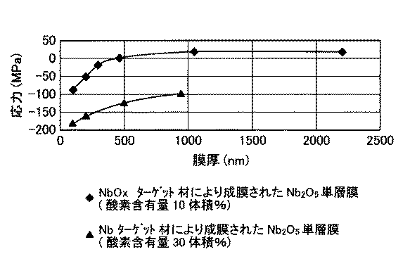
表1から、DCスパッタリングにおいて、酸素が不足しているNbOx をターゲット材に用いる場合は、Nb金属をターゲット材に用いる場合に比べ、応力が緩和された(応力が低い)Nb2 O5 膜が成膜できる。このことは、膜厚の変化に対する、NbOx をターゲット材に用いた場合のNb2 O5 単層膜と、Nb金属をターゲット材に用いた場合のNb2 O5 単層膜の応力を比較した図1からも明らかである。なお、図1において、応力がプラス(+)側にあるときは引張応力であり、マイナス(−)側にあるときは圧縮応力である。また表1から、酸素ガスが不足しているNbOx をターゲット材に用いる場合は、Nb金属ターゲット材に用いる場合に比べ、成膜速度が高速度であることが明らかである。
またTiOx ターゲット材を用いた場合には、Ti金属をターゲット材に用いた場合に比べ、応力が緩和されたTiO2 膜が高速度で成膜できることが明らかである。
【0043】
(実施例1)
参考例1に用いたNbOx ターゲット材を、参考例1と同様に、マグネトロンDCスパッタリング装置に取り付けた。1.1mm厚のガラス基板および0.525mm厚で直径10cmのシリコン基板のそれぞれに、投入電力をDC0.75kW、背圧を1×10⁻³Pa、スパッタリング圧力を0.6Paとし、雰囲気中の酸素ガスとアルゴンガスとの総量に対する酸素ガスの割合を表2に示すように調整してスパッタリングを行い、膜厚200nmのNb2 O5 膜の成膜を行った。
【0044】
次に、同じマグネトロンDCスパッタリング装置を用い、市販のSi(Bドーブ)をターゲット材に用い、雰囲気中の酸素ガスとアルゴンガスとの総量に対する酸素ガスの割合を表2に示すように調整する以外はNbOx ターゲット材のスパッタリング条件と同じ条件でスパッタリングを行い、基板上のNb2 O5 膜の上に膜厚240nmのSiO2 膜を成膜して多層膜(2層)付きの基板を得た。多層膜の特性を参考例1と同様に測定し、その結果を表2に示した。
【0045】
(実施例2〜3)
実施例1において、Nb2 O5 膜およびSiO2 膜の成膜のためのスパッタリングを5回または10回繰返してNb2 O5 膜とSiO2 膜を積層する以外は、実施例1と同様にスパッタリングを行い、多層膜(10層または20層)付き基板を得た。多層膜の特性を参考例1と同様に測定し、その結果を表2に示した。
【0046】
(実施例4)
参考例12に用いたTiOx ターゲット材を、実施例1と同様に、マグネトロンDCスパッタリング装置に取り付けた。1.1mm厚のガラス基板および0.525mm厚で直径10cmのシリコン基板のそれぞれに、投入電力をDC0.75kW、背圧を1×10⁻³Pa、スパッタリング圧力を0.6Paとし、雰囲気中の酸素ガスとアルゴンガスとの総量に対する酸素ガスの割合を表2に示すように調整してスパッタリングを行い、膜厚200nmのTiO2 膜の成膜を行った。
【0047】
次に、同じマグネトロンDCスパッタリング装置を用い、市販のSi(Bドーブ)をターゲット材に用い、雰囲気中の酸素ガスとアルゴンガスとの総量に対する酸素ガスの割合を表2に示すように調整する以外はTiOx ターゲット材のスパッタリング条件と同じ条件でスパッタリングを行い、基板上のTiO2 膜の上に膜厚240nmのSiO2 膜を成膜して多層膜(2層)付きの基板を得た。多層膜の特性を参考例1と同様に測定し、その結果を表2に示した。
【0048】
(実施例5)
実施例4において、TiO2 膜とSiO2 膜との成膜のためのスパッタリングを5回繰返す以外は、実施例4と同様にスパッタリングを行い、多層膜(10層)付き基板を得た。多層膜の特性を参考例1と同様に測定し、その結果を表2に示した。
【0049】
(比較例1)
実施例1のNbOx ターゲット材の代わりに、市販のNb金属をターゲット材に用い、雰囲気中の酸素ガスとアルゴンガスとの総量に対する酸素ガスの割合を表2に示すように調整する以外は実施例1と同様に、スパッタリングを行い、膜厚200nmのNb2 O5 膜の成膜を行った。
次に、同じマグネトロンDCスパッタリング装置を用い、市販のSi(Bドーブ)をターゲット材に用い、雰囲気中の酸素ガスとアルゴンガスとの総量に対する酸素ガスの割合を表2に示すように調整する以外はNb金属ターゲット材のスパッタリング条件と同じ条件でスパッタリングを行い、基板上のNb2 O5 膜の上に膜厚240nmのSiO2 膜を成膜して多層膜(2層)付きの基板を得た。多層膜の特性を参考例1と同様に測定し、その結果を表2に示した。
【0050】
(比較例2)
比較例1において、Nb2 O5 膜とSiO2 膜との成膜のためのスパッタリングを5回繰返して積層する以外は、比較例1と同様にスパッタリングを行い、多層膜(10層)付き基板を得た。多層膜の特性を参考例1と同様に測定し、その結果を表2に示した。
【0051】
(比較例3)
実施例4のTiOx ターゲット材の代わりに、市販のTi金属をターゲット材に用い、雰囲気中の酸素ガスとアルゴンガスとの総量に対する酸素ガスの割合を表2に示すように調整する以外は実施例4と同様に、スパッタリングを行い、膜厚200nmのTiO2 膜の成膜を行った。
次に、同じマグネトロンDCスパッタリング装置を用い、市販のSi(Bドーブ)をターゲット材に用い、雰囲気中の酸素ガスとアルゴンガスとの総量に対する酸素ガスの割合を表2に示すように調整する以外はTi金属ターゲット材のスパッタリング条件と同じ条件でスパッタリングを行い、基板上のTiO2 膜の上に膜厚240nmのSiO2 膜を成膜して多層膜(2層)付きの基板を得た。多層膜の特性を参考例1と同様に測定し、その結果を表2に示した。
【0052】
(比較例4)
比較例3において、TiO2 膜とSiO2 膜との成膜のためのスパッタリングを5回繰返して積層する以外は、比較例3と同様にスパッタリングを行い、多層膜(10層)付き基板を得た。多層膜の特性を参考例1と同様に測定し、その結果を表2に示した。
【0053】
【表2】
【0054】
表2から、DCスパッタリングにおいて、酸素が不足しているNbOx をターゲット材に用いる場合は、Nb金属をターゲット材に用いる場合に比べ、応力が緩和された(応力が低い)Nb2 O5 膜とSiO2 膜との多層膜が成膜できることが明らかである。
またTiOx ターゲット材を用いた場合にも、Ti金属をターゲット材に用いた場合に比べ、応力が緩和されたTiO2 膜とSiO2 膜との多層膜が成膜できることが明らかである。
【0055】
【発明の効果】
本発明に使用されるターゲット材は、導電性を有しているため、スパッタリング法、特にDCスパッタリング法を採用することができるので、生産性がよく、加えて、従来スパッタリング法では得られなかった応力が緩和された大面積の透明金属酸化物膜と二酸化ケイ素膜との多層膜を成膜することができる。したがって、本発明の応力が緩和された透明金属酸化物膜の多層膜は、厚いにもかかわらず反りが少ないので、反射防止膜、反射増加膜、干渉フィルタ、偏光膜などに好適に使用される。
【図面の簡単な説明】
【図1】 DCスパッタリング法によるNb2 O5 単層膜の膜厚と膜の応力との関係を示すグラフ。[0001]
BACKGROUND OF THE INVENTION
The present invention relates to a single layer film of a metal oxide film in which the stress of the film is relaxed by sputtering, a substrate with a multilayer film of a metal oxide film and a silicon dioxide film, and a method for manufacturing the substrate with the film. .
[0002]
[Prior art]
The optical application of metal oxide thin films starts with a single layer of heat-reflective glass or anti-reflection coating, and is further designed to reflect or transmit light of a specific wavelength selectively. It covers many fields such as increased coating, interference filters, and polarizing films. The spectral characteristics of the multilayer film are optically designed with the refractive index n and film thickness of each layer as parameters, and are generally adjusted by combining a high refractive index film and a low refractive index film. In order to realize excellent optical characteristics, it is better that the difference in refractive index n between the high refractive index film and the low refractive index film is large. For example, n = 2.4 titanium dioxide, n = 2.3 five Preferred is a combination of niobium oxide, n = 2.1 tantalum pentoxide, or n = 2.0 tungsten trioxide and n = 1.38 magnesium fluoride or n = 1.46 silicon dioxide. is there. These single layer films and multilayer films can be formed by a vacuum deposition method, a coating method, or the like.
[0003]
On the other hand, when a single layer film or a multilayer film is formed on a large area substrate such as architectural glass, automotive glass, CRT or flat display, a sputtering method, particularly a direct current (DC) sputtering method may be used. Many.
By the way, in the case of forming a high refractive index film by a DC sputtering method, the current situation is so-called reactive sputtering, in which a conductive metallic target is used and sputtering is performed in an atmosphere containing oxygen. However, the film formation rate of the thin film obtained by this method is extremely slow, and there is a problem that the productivity is poor and the cost is high.
[0004]
In order to avoid this, it is conceivable to apply a high sputtering power, but if the target material cannot keep up with cooling, there is a high possibility that troubles such as cracking and peeling will occur. There was a limit. In addition, since the stress of the obtained metal oxide film is high, it may cause warpage of the substrate with the film. In particular, when a multilayer film formed by alternately laminating metal oxide films and silicon dioxide films is provided on a thin substrate, the warpage tends to increase as the total film thickness increases. Therefore, a measure is taken such that a film is finally formed on a thicker substrate than necessary to prevent warping, and after cutting to a desired size, the substrate is polished to a required thickness.
[0005]
In addition, the metal oxide MO lacking oxygen from the stoichiometric composition. x (However, M represents at least one metal selected from the group consisting of Ti, Nb, Ta, Mo, W, Zr and Hf) as a target material, and a transparent metal having a high refractive index by DC sputtering. A method of forming an oxide film on a transparent substrate has also been proposed (see, for example, Patent Document 1). However, this publication does not describe any warping or stress of the film.
[0006]
[Patent Document 1]
International Publication Number (Republished Patent) No. 97/08359
[0007]
[Problems to be solved by the invention]
In the present invention, a multilayer film of a metal oxide film and a silicon dioxide film is formed on a substrate at high speed by a sputtering method using a conductive sputtering material, and the stress of the film is reduced, that is, low stress. It is an object of the present invention to provide a substrate with a multilayer film and a method for producing such a substrate with a low stress multilayer film. In order to obtain a substrate with a film with less warping of the substrate, the stress of the substrate with a multilayer film in which the metal oxide film and the silicon dioxide film are laminated needs to be −100 MPa to +100 MPa, preferably − 60 MPa to +60 MPa, particularly preferably −30 MPa to +30 MPa. When the stress is on the plus (+) side, it is a tensile stress, and when the stress is on the minus (−) side, it is a compressive stress.
[0008]
[Means for Solving the Problems]
The present invention is a substrate with a multilayer film formed by repeatedly laminating at least a metal oxide film and a silicon dioxide film on a substrate at least once, wherein at least one layer of the metal oxide film is chemically Metal oxide MO lacking oxygen than stoichiometric composition x (However, M represents at least one metal selected from the group consisting of Ti, Nb, Ta, Mo, W, Zr, and Hf) as a target material and oxygen deficiency formed by sputtering. And a multilayer oxide film with a multilayer film, wherein the multilayer film has a stress of −100 MPa to +100 MPa.
[0009]
The multilayer film-coated substrate of the present invention comprises a metal oxide MO. x When the metal M is Nb and / or Ta, X is preferably 2 <X <2.5.
[0010]
Further, the substrate with a multilayer film of the present invention comprises a metal oxide MO. x In the case where the metal M is at least one metal selected from the group consisting of Ti, Zr and Hf, X is preferably 1 <X <2.
[0011]
Further, the substrate with a multilayer film of the present invention comprises a metal oxide MO. x When the metal M is Mo and / or W, X is preferably 2 <X <3.
[0012]
In the substrate with a multilayer film of the present invention, the multilayer film preferably has a stress of −60 MPa to +60 MPa.
[0013]
The multilayer film-coated substrate of the present invention is preferably formed by repeatedly laminating the metal oxide film and the silicon dioxide film 10 times or more.
[0014]
The present invention relates to a method for manufacturing a substrate with a multilayer film in which at least a metal oxide film and a silicon dioxide film are alternately laminated, wherein at least one of the metal oxide films is deficient in oxygen from the stoichiometric composition. Metal oxide MO x (Wherein M represents at least one metal selected from the group consisting of Ti, Nb, Ta, Mo, W, Zr and Hf) is used as a target material to form a film, and the multilayer A method for producing a substrate with a multilayer film, wherein the stress of the film is -100 MPa to +100 MPa.
[0015]
DETAILED DESCRIPTION OF THE INVENTION
The substrate with a multilayer film of the present invention is a metal oxide MO in which oxygen is deficient in the stoichiometric composition. x Is used as a target material and sputtering is performed to form a metal oxide film in which oxygen deficiency is eliminated on a substrate.
The target material used to obtain the metal oxide film in the present invention is a metal oxide, and the metal oxide MO is deficient in oxygen from the stoichiometric composition. x (M represents at least one metal selected from the group consisting of Ti, Nb, Ta, Mo, W, Zr, and Hf), and may contain two or more metals M.
[0016]
When M is Nb and / or Ta, X is preferably 2 <X <2.5. This is because when X is 2.5, Nb and / or Ta are completely oxidized, so that the target material is electrically insulating and cannot be subjected to DC sputtering. When X is 2 or less, NbO x And / or TaO x Is chemically unstable and is not preferred as a target material. NbO x Can be used to achieve a high deposition rate, and TaO x When is used, a film having high corrosion resistance and high scratch resistance can be formed.
[0017]
For the same reason as described above, the MO of the target material of the present invention x When M of Mo is Mo and / or W, X is preferably 2 <X <3.
[0018]
Also, the MO of the target material of the present invention x In the case where M is at least one metal selected from the group consisting of Ti, Zr and Hf, X preferably satisfies 1 <X <2.
[0019]
The target material used for obtaining the metal oxide film in the present invention includes a metal oxide MO. x Unless the characteristics including the relaxation of the film stress due to the x By adding an oxide of a metal other than the metal M constituting the film, the film performance such as the refractive index, mechanical properties, and chemical properties can be improved. Examples of such a metal oxide include oxides of at least one metal selected from the group consisting of Cr, Ce, Y, Si, Al, and B. They do not have to be oxygen deficient. For example, in the case of an oxide of Cr, the corrosion resistance of the film is improved, and in the case of an oxide of Ce, an ultraviolet cut property can be imparted to the metal oxide film.
[0020]
The target material used for obtaining the metal oxide film in the present invention is, for example, NbO. x However, in the case of 2 <X <2.5, it is manufactured as follows. There is essentially no change in the case of other metal oxides.
Nb 2 O Five NbO lacking oxygen than its stoichiometric composition (oxygen deficient) by sintering the powder by hot pressing (high temperature high pressure pressing) in a non-oxidizing atmosphere x (However, 2 <X <2.5) is manufactured. Nb 2 O Five The particle size of the powder is suitably 0.05 to 40 μm. It is important that the hot press atmosphere be a non-oxidizing atmosphere, and argon and nitrogen are preferable because the oxygen content of the target material can be easily adjusted. Hydrogen can also be added. The hot press conditions are not particularly limited, but the temperature is preferably 800 to 1400 ° C. and the pressure is 4.90 × 10 6. 6 ~ 9.80x10 6 Pa is preferred.
NbO x The density of the sintered body is 4.0 to 4.4 g / cm. Three The specific resistance is about 0.1 to 0.3 Ωcm.
TiO x The density of the sintered body is 3.8 to 4.2 g / cm Three The specific resistance is about 0.1 to 0.4 Ωcm.
[0021]
In addition, an undercoat made of a metal or alloy is applied on the substrate, and the metal oxide is made into a semi-molten state in a high-temperature plasma gas under a reducing atmosphere, and the semi-melt is undercoated with this gas. It is also possible to obtain a target material used in the present invention consisting of a metal oxide that is deficient in oxygen from the stoichiometric composition by forming a metal oxide by plasma spraying that is transported and deposited thereon. it can.
[0022]
In the present invention, the substrate on which the metal oxide film is formed is not particularly limited, and may be glass, a resin film, silicon, or the like.
[0023]
The substrate with a multilayer film including the metal oxide film in which the stress of the film of the present invention is relaxed is produced by, for example, the following method, but is not limited thereto.
[0024]
The target material used for obtaining the metal oxide film in the present invention is composed of a metal oxide, and is slightly oxygen-deficient from the stoichiometric composition. Therefore, when a metal oxide film is formed, a metal oxide film in which the oxygen deficiency is eliminated can be obtained by supplementing the sputtering atmosphere with oxygen that is slightly insufficient from the stoichiometric composition. .
[0025]
For example, a metal oxide that is slightly oxygen-deficient slightly from the stoichiometric composition is used as a target material, and the pressure is 0.15 to 1 in an argon atmosphere or a mixed atmosphere of argon and a small amount of oxygen. When DC sputtering is performed at about 5 Pa, a uniform transparent film, that is, a metal oxide film in which oxygen deficiency is eliminated can be formed on the substrate at high speed. When using a metal target, a change in oxygen partial pressure causes a hysteresis phenomenon that is a discontinuous change in film formation rate and discharge current / voltage, but when the metal oxide is used as a target material, Such a hysteresis phenomenon does not occur, it is relatively easy to control the film formation rate during film formation, and the amount of oxygen gas to be supplied can be reduced to a necessary minimum or close to it.
[0026]
When the proportion of oxygen decreases, the metal oxide film tends to be close to the metal film and become an absorption film. Conversely, when the proportion of oxygen increases, the deposition rate decreases, and the stress of the metal oxide film tends to become a large compressive stress. Therefore, adjustment of the partial pressure of oxygen is important, and it is preferable that 0 to 30% by volume of oxygen is contained in the sputtering gas. However, NbO x In the target material using, it is preferable that 1 to 30% by volume of oxygen is contained in the sputtering gas. When a metal target material is used, although depending on input power, it is preferable that oxygen is contained in the sputtering gas in an amount of 30% by volume or more in order not to form an absorption film.
[0027]
The thickness of the metal oxide film to be formed is adjusted by the sputtering time, input power, etc., but the thickness of one layer of the metal oxide film is preferably 10 to 1000 nm, particularly preferably 10 to 300 nm.
A metal oxide film formed from a metal oxide target lacking oxygen has the same optical characteristics as the refractive index compared to a metal oxide film formed from a normal metal target. The film is relaxed in stress. The reason for this is not clear, but it is presumed that the film growth process during film formation is different.
[0028]
Next, on the substrate with the film on which the metal oxide film is formed, silicon is further used as a target material, and sputtering is performed in the same manner as in the case where the metal oxide is used as the target material. A silicon film is formed. The outermost layer may be a metal oxide film or a silicon dioxide film. The innermost layer may also be a metal oxide film or a silicon dioxide film. Further, a third film different from the metal oxide film and the silicon dioxide film can be interposed so that the multilayer film can cope with various characteristics. For example, an aluminum oxide film having a medium refractive index may be interposed in order to satisfy optical conditions.
[0029]
A metal oxide film and a silicon dioxide film can be repeatedly laminated one or more times, such as 5 times, 10 times, or 50 times, to form a multilayer film exceeding 100 layers. Therefore, although the film thickness of the multilayer film is increased by the number of layers, since the stress of the metal oxide film cancels the stress of the silicon dioxide film to some extent, even when the multilayer film is formed, the warp is extremely small. This means that it is not necessary to increase the thickness of the substrate in order to suppress warpage when manufacturing a multilayer film, and the polishing step of the substrate with the multilayer film after film formation is omitted or reduced. This greatly contributes to an increase in the number of film layers and cost reduction. The thickness of one layer of the metal oxide film of the substrate with a multilayer film is preferably 10 to 1000 nm, particularly preferably 10 to 300 nm, and the thickness of one layer of the silicon dioxide film is 10 to 1000 nm, particularly 10 to 300 nm. Is preferred.
[0030]
The above describes the case where a metal oxide film is first formed on a substrate, then a silicon dioxide film is formed, and the silicon dioxide film is the outermost layer. In addition, when a silicon dioxide film is formed, and then a metal oxide film is formed, there is no change in the formation of each layer, and the description is omitted. For example, a three-layer film composed of a metal oxide film, a silicon dioxide film and a metal oxide film, or a five-layer film obtained by further laminating a silicon dioxide film and a metal oxide film on the three-layer film is also convenient. It is included in the substrate with a multilayer film of the present invention formed by repeatedly laminating at least once.
[0031]
The metal oxide film-coated substrate thus obtained is used for various applications. Although the film formation of the substrate with a multilayer film by DC sputtering has been described above, the same process is performed for the film formation of a substrate with a multilayer film by alternating current (AC) sputtering.
[0032]
【Example】
EXAMPLES Hereinafter, although an Example demonstrates this invention, of course, this invention is not limited to these Examples.
[0033]
(Production Example 1)
(NbO x Sintered body)
Commercially available high purity Nb 2 O Five The powder was filled in a carbon hot press mold and held at 1100 ° C. for 1 hour in an argon atmosphere, and then pressure 4.903 × 10 6. 6 Hot pressing was performed with Pa to obtain a sintered body. The density and specific resistance of the sintered body were measured.
Next, the sintered body was pulverized in an agate mortar, heated in air to 1100 ° C., and the mass of the sintered body before and after heating was measured. By this heating, NbO in a state where oxygen is insufficient due to the previous sintering. x Sintered body Nb completely oxidized from 2 O Five From the increase in mass, the oxygen content of the sintered body was calculated, and oxygen deficiency was confirmed.
The density of the sintered body is 4.00 g / cm Three The specific resistance is 0.30 Ωcm and the oxygen content is NbO x The X of 2.498 was 2.498.
[0034]
(Production Example 2)
(TiO x Sintered body)
High purity Nb of Production Example 1 2 O Five Commercial high-purity TiO instead of powder 2 Except using powder, the sintered compact was obtained by the same method and conditions as the manufacture example 1, and the density and specific resistance of the sintered compact were measured.
Next, it heated by the method and conditions similar to manufacture example 1, the mass of the sintered compact before and behind a heating was measured, the oxygen content of the sintered compact was calculated from the mass increase, and oxygen deficiency was confirmed. The density of the sintered body is 3.90 g / cm Three The specific resistance is 0.35 Ωcm and the oxygen content is TiO x X of 1.980 was 1.980.
[0035]
(Reference Examples 1-6)
NbO produced by Production Example 1 x The sintered body was ground into a rectangular parallelepiped having a size of 200 mm × 70 mm and a thickness of 5 mm to produce a target material. This target material was bonded to a copper packing plate with a metal bond and attached to a magnetron DC sputtering apparatus. Each of a glass substrate of 1.1 mm thickness and a silicon substrate of 0.525 mm thickness and 10 cm in diameter has an input power of DC 0.75 kW and a back pressure of 1 × 10 -3 Sputtering was carried out by adjusting the ratio of oxygen gas to the total amount of oxygen gas and argon gas in the atmosphere as shown in Table 1, and sputtering with a Pa and sputtering pressure of 0.6 Pa. 2 O Five A film was formed. The discharge during sputtering was extremely stable, and the film could be stably formed even by DC sputtering.
[0036]
After film formation, the film thickness was measured using a stylus type film thickness measuring device.
The stress of the film was determined by measuring the warp (curvature radius) of a silicon substrate having a diameter of 10 cm before and after film formation, using FleXus F2320 which is FLX THIN FILMS STRESS MEASUREMENT SYSTEM of Tencor Instruments. .
The refractive index of the film on the glass substrate was measured with JAWoollam Co., Inc. spectroscopic ellipsometer WVASE32. The film was transparent and the film did not absorb light.
Table 1 shows the film thickness, film formation speed, film stress, and film refractive index at a wavelength of 550 nm.
[0037]
(Reference Examples 7 to 11)
NbO in Reference Example 1 x Instead of the target material, a commercially available Nb metal is used as the target material, and the ratio of oxygen gas to the total amount of oxygen gas and argon gas in the atmosphere is adjusted as shown in Table 1, as in Reference Example 1, Sputtering and Nb 2 O Five A film was formed. The discharge during sputtering was extremely stable, and the film could be stably formed even by DC sputtering. Nb 2 O Five The film characteristics were measured in the same manner as in Reference Example 1, and the results are shown in Table 1.
[0038]
(Reference Examples 12-14)
TiO produced by Production Example 2 x The sintered body was ground into a rectangular parallelepiped having a size of 200 mm × 70 mm and a thickness of 5 mm to produce a target material. This target material was bonded to a copper packing plate with a metal bond and attached to a magnetron DC sputtering apparatus. Each of a glass substrate of 1.1 mm thickness and a silicon substrate of 0.525 mm thickness and 10 cm in diameter has an input power of DC 0.75 kW and a back pressure of 1 × 10 -3 Sputtering was performed by adjusting the ratio of oxygen gas to the total amount of oxygen gas and argon gas in the atmosphere as shown in Table 1, and sputtering with a film thickness of TiO as shown in Table 1. 2 A film was formed. The discharge during sputtering was extremely stable, and the film could be stably formed even by DC sputtering.
[0039]
(Reference Examples 15 to 16)
TiO of Reference Example 12 x Instead of the target material, using commercially available Ti metal as the target material, except that the ratio of oxygen gas to the total amount of oxygen gas and argon gas in the atmosphere is adjusted as shown in Table 1, as in Reference Example 12, Sputtering and TiO 2 A film was formed. The discharge during sputtering was extremely stable, and the film could be stably formed even by DC sputtering. TiO 2 The film characteristics were measured in the same manner as in Reference Example 1, and the results are shown in Table 1.
[0040]
(Reference Examples 17-18)
NbO in Reference Example 1 x Reference Example 1 except that commercially available Si (B dove) is used for the target material instead of the target material, and the ratio of oxygen gas to the total amount of oxygen gas and argon gas in the atmosphere is adjusted as shown in Table 1. Similarly, sputtering is performed to obtain SiO. 2 A film was formed. SiO 2 The film characteristics were measured in the same manner as in Reference Example 1, and the results are shown in Table 1.
[0041]
[Table 1]
[0042]
From Table 1, NbO lacking oxygen in DC sputtering. x Is used for the target material, the stress is relaxed (stress is low) compared to the case where Nb metal is used for the target material. 2 O Five A film can be formed. This means that NbO against the change in film thickness x When Nb is used as a target material 2 O Five Single layer film and Nb when Nb metal is used as target material 2 O Five It is clear from FIG. 1 that compares the stresses of the single layer films. In FIG. 1, when the stress is on the plus (+) side, it is a tensile stress, and when it is on the minus (−) side, it is a compressive stress. Also, from Table 1, NbO lacking oxygen gas x It is apparent that the film formation rate is higher when the film is used for the target material than when the film is used for the Nb metal target material.
TiO x When the target material is used, the stress is relaxed compared with the case where Ti metal is used as the target material. 2 It is clear that the film can be deposited at high speed.
[0043]
(Example 1)
NbO used in Reference Example 1 x The target material was attached to a magnetron DC sputtering apparatus as in Reference Example 1. Each of a glass substrate of 1.1 mm thickness and a silicon substrate of 0.525 mm thickness and 10 cm in diameter has an input power of DC 0.75 kW and a back pressure of 1 × 10 -3 Sputtering was carried out by adjusting the ratio of oxygen gas to the total amount of oxygen gas and argon gas in the atmosphere as shown in Table 2 with a Pa and sputtering pressure of 0.6 Pa. 2 O Five A film was formed.
[0044]
Next, using the same magnetron DC sputtering apparatus, commercially available Si (B dove) is used as a target material, and the ratio of oxygen gas to the total amount of oxygen gas and argon gas in the atmosphere is adjusted as shown in Table 2. Is NbO x Sputtering is performed under the same conditions as the sputtering conditions of the target material, and Nb on the substrate 2 O Five 240 nm thick SiO on the film 2 A film was formed to obtain a substrate with a multilayer film (two layers). The characteristics of the multilayer film were measured in the same manner as in Reference Example 1, and the results are shown in Table 2.
[0045]
(Examples 2-3)
In Example 1, Nb 2 O Five Membrane and SiO 2 Sputtering for film formation is repeated 5 or 10 times to obtain Nb 2 O Five Film and SiO 2 Except for laminating the films, sputtering was performed in the same manner as in Example 1 to obtain a substrate with a multilayer film (10 layers or 20 layers). The characteristics of the multilayer film were measured in the same manner as in Reference Example 1, and the results are shown in Table 2.
[0046]
Example 4
TiO used in Reference Example 12 x The target material was attached to a magnetron DC sputtering apparatus in the same manner as in Example 1. Each of a glass substrate of 1.1 mm thickness and a silicon substrate of 0.525 mm thickness and 10 cm in diameter has an input power of DC 0.75 kW and a back pressure of 1 × 10 -3 Sputtering was carried out by adjusting the ratio of oxygen gas to the total amount of oxygen gas and argon gas in the atmosphere as shown in Table 2, with a Pa and sputtering pressure of 0.6 Pa, and with a TiO2 film thickness of 200 nm. 2 A film was formed.
[0047]
Next, the same magnetron DC sputtering apparatus is used, commercially available Si (B dove) is used as a target material, and the ratio of oxygen gas to the total amount of oxygen gas and argon gas in the atmosphere is adjusted as shown in Table 2. Is TiO x Sputtering is performed under the same conditions as the sputtering conditions of the target material. 2 240 nm thick SiO on the film 2 A film was formed to obtain a substrate with a multilayer film (two layers). The characteristics of the multilayer film were measured in the same manner as in Reference Example 1, and the results are shown in Table 2.
[0048]
(Example 5)
In Example 4, TiO 2 Film and SiO 2 Sputtering was performed in the same manner as in Example 4 except that sputtering for film formation was repeated 5 times to obtain a substrate with a multilayer film (10 layers). The characteristics of the multilayer film were measured in the same manner as in Reference Example 1, and the results are shown in Table 2.
[0049]
(Comparative Example 1)
NbO of Example 1 x Instead of the target material, a commercially available Nb metal is used as the target material, and the ratio of oxygen gas to the total amount of oxygen gas and argon gas in the atmosphere is adjusted as shown in Table 2, as in Example 1, Sputtering is performed to form a 200 nm thick Nb. 2 O Five A film was formed.
Next, using the same magnetron DC sputtering apparatus, commercially available Si (B dove) is used as a target material, and the ratio of oxygen gas to the total amount of oxygen gas and argon gas in the atmosphere is adjusted as shown in Table 2. Is sputtered under the same sputtering conditions as the Nb metal target material, and Nb on the substrate 2 O Five 240 nm thick SiO on the film 2 A film was formed to obtain a substrate with a multilayer film (two layers). The characteristics of the multilayer film were measured in the same manner as in Reference Example 1, and the results are shown in Table 2.
[0050]
(Comparative Example 2)
In Comparative Example 1, Nb 2 O Five Film and SiO 2 Sputtering was performed in the same manner as in Comparative Example 1 except that the sputtering for film formation was repeated 5 times to obtain a substrate with a multilayer film (10 layers). The characteristics of the multilayer film were measured in the same manner as in Reference Example 1, and the results are shown in Table 2.
[0051]
(Comparative Example 3)
TiO in Example 4 x Instead of the target material, commercially available Ti metal is used as the target material, and the ratio of oxygen gas to the total amount of oxygen gas and argon gas in the atmosphere is adjusted as shown in Table 2, as in Example 4, Sputtering is performed to form TiO with a film thickness of 200 nm. 2 A film was formed.
Next, using the same magnetron DC sputtering apparatus, commercially available Si (B dove) is used as a target material, and the ratio of oxygen gas to the total amount of oxygen gas and argon gas in the atmosphere is adjusted as shown in Table 2. Sputters under the same conditions as the sputtering conditions for the Ti metal target material, and TiO on the substrate 2 240 nm thick SiO on the film 2 A film was formed to obtain a substrate with a multilayer film (two layers). The characteristics of the multilayer film were measured in the same manner as in Reference Example 1, and the results are shown in Table 2.
[0052]
(Comparative Example 4)
In Comparative Example 3, TiO 2 Film and SiO 2 Sputtering was performed in the same manner as in Comparative Example 3 except that sputtering for film formation was repeated 5 times to obtain a substrate with a multilayer film (10 layers). The characteristics of the multilayer film were measured in the same manner as in Reference Example 1, and the results are shown in Table 2.
[0053]
[Table 2]
[0054]
From Table 2, NbO lacking oxygen in DC sputtering. x Is used for the target material, the stress is relaxed (stress is low) compared to the case where Nb metal is used for the target material. 2 O Five Film and SiO 2 It is clear that a multilayer film with a film can be formed.
TiO x Even when the target material is used, the stress is relaxed compared with the case where Ti metal is used as the target material. 2 Film and SiO 2 It is clear that a multilayer film with a film can be formed.
[0055]
【The invention's effect】
Since the target material used in the present invention has conductivity, a sputtering method, in particular, a DC sputtering method can be adopted, so that the productivity is good, and in addition, it has not been obtained by the conventional sputtering method. A multilayer film of a transparent metal oxide film and a silicon dioxide film having a large area with reduced stress can be formed. Therefore, the multilayer film of the transparent metal oxide film in which the stress of the present invention is relieved is less warped despite being thick, and thus is suitably used for an antireflection film, a reflection increasing film, an interference filter, a polarizing film, and the like. .
[Brief description of the drawings]
FIG. 1 Nb by DC sputtering method 2 O Five The graph which shows the relationship between the film thickness of a single layer film, and the stress of a film | membrane.