JP2005295556A - 量子化装置用ディザ回路 - Google Patents
量子化装置用ディザ回路 Download PDFInfo
- Publication number
- JP2005295556A JP2005295556A JP2005099842A JP2005099842A JP2005295556A JP 2005295556 A JP2005295556 A JP 2005295556A JP 2005099842 A JP2005099842 A JP 2005099842A JP 2005099842 A JP2005099842 A JP 2005099842A JP 2005295556 A JP2005295556 A JP 2005295556A
- Authority
- JP
- Japan
- Prior art keywords
- signal
- dither
- digital
- digital format
- circuit
- Prior art date
- Legal status (The legal status is an assumption and is not a legal conclusion. Google has not performed a legal analysis and makes no representation as to the accuracy of the status listed.)
- Granted
Links
Images
Classifications
-
- H—ELECTRICITY
- H03—ELECTRONIC CIRCUITRY
- H03M—CODING; DECODING; CODE CONVERSION IN GENERAL
- H03M1/00—Analogue/digital conversion; Digital/analogue conversion
- H03M1/06—Continuously compensating for, or preventing, undesired influence of physical parameters
- H03M1/0617—Continuously compensating for, or preventing, undesired influence of physical parameters characterised by the use of methods or means not specific to a particular type of detrimental influence
- H03M1/0634—Continuously compensating for, or preventing, undesired influence of physical parameters characterised by the use of methods or means not specific to a particular type of detrimental influence by averaging out the errors, e.g. using sliding scale
- H03M1/0636—Continuously compensating for, or preventing, undesired influence of physical parameters characterised by the use of methods or means not specific to a particular type of detrimental influence by averaging out the errors, e.g. using sliding scale in the amplitude domain
- H03M1/0639—Continuously compensating for, or preventing, undesired influence of physical parameters characterised by the use of methods or means not specific to a particular type of detrimental influence by averaging out the errors, e.g. using sliding scale in the amplitude domain using dither, e.g. using triangular or sawtooth waveforms
-
- H—ELECTRICITY
- H03—ELECTRONIC CIRCUITRY
- H03M—CODING; DECODING; CODE CONVERSION IN GENERAL
- H03M1/00—Analogue/digital conversion; Digital/analogue conversion
- H03M1/12—Analogue/digital converters
Landscapes
- Engineering & Computer Science (AREA)
- Theoretical Computer Science (AREA)
- Analogue/Digital Conversion (AREA)
Abstract
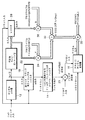
【解決手段】 3分周回路12がADC用のサンプリング・クロックから[サンプリング周波数]/3の周波数の信号を発生し、この信号を再タイミング用レジスタ18及びフィルタ14により処理してディザ信号を発生する。加算器20がデジタル化されるアナログ信号とディザ信号とを組み合わせて、ADC16に供給する。ブロック22、24、26、28、30により、ディザ信号のデジタル形式信号からキャンセル信号を発生し、加算回路32がキャンセル信号をADCのデジタル出力信号と組み合わせて、量子化歪が減少した補正済のデジタル出力信号を発生する。
【選択図】図1
Description
(a)周期Tの総ての繰り返し信号が、直流オフセットと、周期Tの基本正弦波と、基本波の高調波との和で表すことができる。
(b)基本波及び高調波の各々が、繰り返し信号の形状により独自に決まる振幅及び位相を有する。
正弦波周波数は、その周期、即ち、サイクル時間と相互関係があるので、その基本波周波数は、1秒当たり1/Tサイクル、即ち、1/Tヘルツである。周期Tの正弦波の高調波の周波数は、基本波周波数の整数倍であるので、n次の高調波は、周波数がn/Tであり、周期がT/nである。
Y(t)=DC+Σn=1-M(A(n,f)sin(2πnft+P(n,f)))
A(n,f)は、基本波周波数のn次高調波の振幅であり、P(n,f)は、対応する位相である。角周波数の単位であるラジアン/秒において2πf=ωであるので、一周、即ち、1サイクルは、2πラジアンである。実現可能なシステムにおいて、高周波数の経路が制限されるので、高い高調波も制限される。例えば、アナログ・システムは、最大駆動電流能力や、容量性付加により制限されるので、実際には、Mが無限にまで広がることはない。よって、繰り返し信号は、Tと、M個の振幅{A}及び位相{P}の有限の2組とにより決まる。
(a)入力信号にわずかな変化があっても、高調波特性に急激な変化が生じる。
(b)入力正弦波が滑らかに変化するならば、高調波は、互いに相対的に変化するが、類似した振幅範囲となる。
(c)高調波特性は、アナログ・システムが可能とする最大帯域幅にまで広がる。
ディザをADCの入力信号に付加することにより、量子化歪を減らすことができる。歪メカニズムは、周期的を基本とする複数の電圧レベルの間における遷移の自然な結果なので、ディザの効果は、ADCへの小さな入力信号によっても量子化歪が生じるという事実に基づく。実際に、量子化歪は、実行するADC量子化ステップのサイズに密接に関連する。
W(t)=(1,0,0,1,0,0,1,0,0,1,・・・)
を発生するか、又は、シーケンス
W(t)=(1,1,0,1,1,0,1,1,0,1,・・・)
を発生するか、又は、fs/3の繰り返し周期の任意の他のシーケンスを発生する。クロック信号は、1及び0のデジタル信号でもあるので、これらシーケンスの信号は、ディザ信号を表す単一ビットのデジタル形式信号、即ち、ディザ信号のデジタル形式信号であり、その高調波を(2fs/3, 3fs/3, 4 fs/3, 5 fs/3, 6 fs/3,・・・)とする。これら周波数は、サンプリング周波数のエリアシング(fs/3, DC, fs/3, fs/3, DC,・・・)を生じる。なお、エリアシングとは、本来ならば通過しない周波数帯域幅よりも上の周波数の高調波の一部のエネルギーが折りたたまれて、この周波数帯域幅内の低い周波数として信号出力に現れ、この信号出力の歪の源となることをいう。このデジタル・シーケンスに作用する簡単なバンドパス又はロウパスのアナログ・フィルタ14は、多段ADC(量子化装置)16に供給する前に、直流(DC)及び大部分の高調波を除去する。なお、総ての非直流高調波がfs/3となるので、フィルタ14の性能はそれほど重要ではない。より重要なことは、フィルタ14の出力信号がADC16によりサンプリングされるので、位相ノイズが小さい低ジッタのレジスタ回路18により直列デジタル・ストリームを再クロックする、即ち、クロックに再び同期させる。(なお、これらブロック12、14及び18は、第1手段を構成する。)アナログ・フィルタ14は、レジスタ回路18からのタイミング調整された直列デジタル・ストリーム(ディザ信号のデジタル形式信号)をフィルタ処理するので、このアナログ・フィルタ14からの結果出力は、fs/3の疑似正弦波(アナログ信号)であり、加算器(第2手段)20に供給される。この加算器20には、デジタル化されるアナログ信号も入力する。加算器20の出力信号がADC16の入力となる。上述の米国特許第4812846号と同様に、アナログ正弦波ディザ入力を発生するこの方法の重要な利点は、高精度のデジタル・アナログ変換器(DAC)が必要ないことである。しかし、各サンプリング時点にて、典型的な3つの異なる加算された電圧レベルが存在し、ディザ効果を高める。
所望位相がpで、2つの値がq=±1及びr=±1ならば、2つの変数S及びCは次のように決まる。
S=rsin(p)
C=qcos(p)
となり、
g(t)=A((S/SQRT(3))-C)cos(2πt/3)+(2AS/SQRT(3))cos(2π(t+1)/3)
となる。なお、SQRTは平方根を意味する。基本的な三角関数の特性を用いて、
g(t)=-qAcos((2πt/3)-qrp)
となる。q=-1及びr=1に対して、
g(t)=Acos((2πt/3)+p)
となる。これは、振幅がAで位相がpのfs/3の余弦波である。よって、
g(t)=Xcos(2πt/3)+Ycos(2π(t+1)/3)
となる。ここで、{X,Y}は次式から得られる。
X=A(cos(p)+sin(p)/SQRT(3))
Y=2Asin(p)/SQRT(3)
{1, -1/2, -1/2, 1, -1/2, -1/2,・・・}
このシーケンスを対比すると、1−>1及び0−>-1/2のマッピングであるので、値変換器22により、3分周回路12の出力信号(デジタル信号のデジタル形式信号)から余弦値を表すデジタル信号(直接デジタル形式信号)を容易に発生できる。限定された1組の値が、掛け算ハードウェア24及び26に必要となる。第2の余弦式を表すデジタル信号は、レジスタ28により1サンプリング・クロック分だけ遅延された単なる上述のシーケンスであり、このシーケンスは、レジスタ28の入力と位相が90度(直角位相)ずれた場合に直角位相デジタル形式信号となる。デジタル的な掛け算ハードウェア24,26からの出力信号は、互いに直角位相(90度)だけずれており、直角位相デジタル成果信号となる。これら出力信号は、デジタル加算器30に供給され、キャンセル信号である余弦波(キャンセル余弦波を表すデジタル信号)を発生する。(これらブロック22、24、26、28及び30が第3手段を構成する。)このキャンセル余弦波をデジタル加算回路(第4手段)32に供給し、ADC16のデジタル出力信号から入力ディザ信号を引き算(負の加算)して、デジタル出力信号における量子化の影響を望ましく低減する。
14 アナログ・フィルタ
16 アナログ・デジタル変換器(量子化装置)
18 レジスタ装置
20 加算器
22 値変換回路
24、26 掛け算回路
28 レジスタ
30 加算器
32 加算回路
Claims (4)
- 量子化装置用のディザ回路であって、
サンプリング周波数のクロック信号から、上記サンプリング周波数の3分の1の周波数のディザ信号を得る第1手段と、
デジタル化されるアナログ信号と上記ディザ信号とを上記量子化装置の入力にて組み合わせる第2手段と、
上記第1手段からの上記ディザ信号のデジタル形式信号からキャンセル信号を発生する第3手段と、
上記キャンセル信号を上記量子化装置からのデジタル出力信号と組み合わせて、量子化歪が減少した補正済のデジタル出力信号を発生する第4手段と
を具えた量子化装置用ディザ回路。 - 上記第1手段は、
入力として上記クロック信号を受け、出力として上記ディザ信号のデジタル形式信号を発生する3分周回路と、
上記ディザ信号のデジタル形式信号をフィルタ処理して、上記第2手段用の入力用に上記ディザ信号を出力するフィルタ手段と
を具えたことを特徴とする請求項1の量子化装置用ディザ回路。 - 上記第1手段は、
上記ディザ信号のデジタル形式信号を入力信号として受け、上記フィルタ手段の入力用に上記ディザ信号のタイミングが変更されたデジタル形式信号を出力する低ジッタ再タイミング用レジスタ
を更に具えたことを特徴とする請求項2の量子化装置用ディザ回路。 - 上記第4手段は、
上記ディザ信号のデジタル形式信号を直接デジタル形式信号に変換する手段と、
上記直接デジタル形式信号を上記クロック信号の1サイクル分だけ遅延させて、直角位相デジタル形式信号を発生する手段と、
上記直接デジタル形式信号及び上記直角位相デジタル形式信号を各々のプログラマブル係数と乗算して、複数の直角位相デジタル成果信号を発生する手段と、
上記複数の直角デジタル成果信号を組み合わせて、上記キャンセル信号を発生する手段と
を具えた請求項1〜3の量子化装置用ディザ回路。
Applications Claiming Priority (1)
| Application Number | Priority Date | Filing Date | Title |
|---|---|---|---|
| US10/817,477 US6950048B1 (en) | 2004-04-02 | 2004-04-02 | Dither system for a quantizing device |
Publications (2)
| Publication Number | Publication Date |
|---|---|
| JP2005295556A true JP2005295556A (ja) | 2005-10-20 |
| JP4076547B2 JP4076547B2 (ja) | 2008-04-16 |
Family
ID=34992654
Family Applications (1)
| Application Number | Title | Priority Date | Filing Date |
|---|---|---|---|
| JP2005099842A Expired - Fee Related JP4076547B2 (ja) | 2004-04-02 | 2005-03-30 | 量子化装置用ディザ回路 |
Country Status (3)
| Country | Link |
|---|---|
| US (1) | US6950048B1 (ja) |
| JP (1) | JP4076547B2 (ja) |
| CN (1) | CN1677868B (ja) |
Cited By (1)
| Publication number | Priority date | Publication date | Assignee | Title |
|---|---|---|---|---|
| JP2010056926A (ja) * | 2008-08-28 | 2010-03-11 | Yamaha Corp | D/a変換回路およびデジタル入力型d級増幅器 |
Families Citing this family (12)
| Publication number | Priority date | Publication date | Assignee | Title |
|---|---|---|---|---|
| WO2009010672A2 (fr) * | 2007-07-06 | 2009-01-22 | France Telecom | Limitation de distorsion introduite par un post-traitement au decodage d'un signal numerique |
| US8068045B2 (en) * | 2010-03-01 | 2011-11-29 | Analog Devices, Inc. | Calibration methods and structures for pipelined converter systems |
| US9306590B2 (en) * | 2011-05-26 | 2016-04-05 | Tektronix, Inc. | Test and measurement instrument including asynchronous time-interleaved digitizer using harmonic mixing |
| US8742749B2 (en) * | 2011-05-26 | 2014-06-03 | Tektronix, Inc. | Test and measurement instrument including asynchronous time-interleaved digitizer using harmonic mixing |
| US9568503B2 (en) * | 2011-05-26 | 2017-02-14 | Tektronix, Inc. | Calibration for test and measurement instrument including asynchronous time-interleaved digitizer using harmonic mixing |
| US9432042B2 (en) | 2011-05-26 | 2016-08-30 | Tektronix, Inc. | Test and measurement instrument including asynchronous time-interleaved digitizer using harmonic mixing |
| US8723707B2 (en) | 2011-11-14 | 2014-05-13 | Analog Devices, Inc. | Correlation-based background calibration for reducing inter-stage gain error and non-linearity in pipelined analog-to-digital converters |
| CN102636696B (zh) * | 2012-05-07 | 2014-04-09 | 上海萌芯电子科技有限公司 | 一种开关电容型模数转换器输入阻抗的测试方法 |
| US8928514B1 (en) | 2013-09-13 | 2015-01-06 | Tektronix, Inc. | Harmonic time domain interleave to extend oscilloscope bandwidth and sample rate |
| CN106257300B (zh) * | 2015-06-19 | 2021-08-06 | 特克特朗尼克公司 | 一种测试和测量仪器和用于确定补偿值的方法 |
| US10659069B2 (en) * | 2018-02-02 | 2020-05-19 | Analog Devices, Inc. | Background calibration of non-linearity of samplers and amplifiers in ADCs |
| US11711198B2 (en) * | 2019-07-25 | 2023-07-25 | Nippon Telegraph And Telephone Corporation | Synchronous detection apparatus, synchronous detection method, and program |
Family Cites Families (10)
| Publication number | Priority date | Publication date | Assignee | Title |
|---|---|---|---|---|
| US4524447A (en) * | 1983-05-25 | 1985-06-18 | Rca Corporation | Digital signal processing apparatus having digital dither |
| JPH07118649B2 (ja) | 1986-01-08 | 1995-12-18 | ヤマハ株式会社 | デイザ回路 |
| US5940138A (en) * | 1992-08-04 | 1999-08-17 | J. Carl Cooper | Analog signal process with dither pattern |
| US5493298A (en) * | 1993-03-01 | 1996-02-20 | Hewlett-Packard Company | Dithered analog-to-digital converter |
| US5825253A (en) * | 1997-07-15 | 1998-10-20 | Qualcomm Incorporated | Phase-locked-loop with noise shaper |
| US5986512A (en) * | 1997-12-12 | 1999-11-16 | Telefonaktiebolaget L M Ericsson (Publ) | Σ-Δ modulator-controlled phase-locked-loop circuit |
| US6268814B1 (en) * | 2000-03-14 | 2001-07-31 | Lucent Technologies Inc. | Carrier-dependent dithering for analog-to-digital conversion |
| WO2002023731A2 (en) * | 2000-09-11 | 2002-03-21 | Broadcom Corporation | Methods and systems for digital dither |
| US6880262B1 (en) * | 2003-09-30 | 2005-04-19 | Broadcom Corporation | Continuous time ΔΣ ADC with dithering |
| US6825784B1 (en) * | 2004-02-18 | 2004-11-30 | Texas Instruments Incorporated | Dithering method for sigma-delta analog-to-digital converters |
-
2004
- 2004-04-02 US US10/817,477 patent/US6950048B1/en not_active Expired - Fee Related
-
2005
- 2005-03-30 JP JP2005099842A patent/JP4076547B2/ja not_active Expired - Fee Related
- 2005-04-01 CN CN200510065147.XA patent/CN1677868B/zh not_active Expired - Fee Related
Cited By (1)
| Publication number | Priority date | Publication date | Assignee | Title |
|---|---|---|---|---|
| JP2010056926A (ja) * | 2008-08-28 | 2010-03-11 | Yamaha Corp | D/a変換回路およびデジタル入力型d級増幅器 |
Also Published As
| Publication number | Publication date |
|---|---|
| US20050219095A1 (en) | 2005-10-06 |
| CN1677868B (zh) | 2010-06-09 |
| US6950048B1 (en) | 2005-09-27 |
| CN1677868A (zh) | 2005-10-05 |
| JP4076547B2 (ja) | 2008-04-16 |
Similar Documents
| Publication | Publication Date | Title |
|---|---|---|
| JP4076547B2 (ja) | 量子化装置用ディザ回路 | |
| Petraglia et al. | Analysis of mismatch effects among A/D converters in a time-interleaved waveform digitizer | |
| KR100787369B1 (ko) | 아날로그-디지털 변환을 위한 캐리어-의존 디더링 | |
| JP4498184B2 (ja) | 直線性補償回路 | |
| US20200373934A1 (en) | Vco-based continuous-time pipelined adc | |
| US6404364B1 (en) | Multistage converter employing digital dither | |
| WO2001067614A1 (en) | Digital cancellation of d/a converter noise in pipelined a/d converters | |
| JPH07162307A (ja) | アナログ−ディジタル変換器 | |
| US6930625B1 (en) | Multi-thread parallel processing sigma-delta ADC | |
| Carley | An oversampling analog-to-digital converter topology for high-resolution signal acquisition systems | |
| TW201937860A (zh) | 餘數產生系統、類比數位轉換器以及產生殘餘訊號之方法 | |
| Kester | What the Nyquist criterion means to your sampled data system design | |
| TW201334424A (zh) | 用於在類比至數位轉換器中將元件不匹配隨機化之系統與方法 | |
| GB2419754A (en) | Analogue to digital converter utilsing analogue dither | |
| JP2023094552A (ja) | 時間インターリーブされたデジタル-アナログ変換器を較正するためのシステムおよび方法 | |
| JP2575642B2 (ja) | アナログ−デジタル コンバ−タ | |
| US9071260B2 (en) | Method and related device for generating a digital output signal corresponding to an analog input signal | |
| Steensgaard-Madsen | High-performance data converters | |
| KR100360632B1 (ko) | 실제선형위상응답을동반한위상각보정의제공및양자화신호들의필터링을위한데시메이션회로및방법 | |
| US10425096B1 (en) | Method and apparatus for improving resolutions of analog-to-digital converters | |
| Hejn et al. | Measurement and enhancement of multistage sigma-delta modulators | |
| Jungwirth et al. | Improved Sayiner level crossing ADC | |
| Oldham | Digital waveform synthesis techniques | |
| Król | Choice of analog-to-digital converters for audio measurements using MLS algorithm | |
| CN1954500B (zh) | 一种△-∑调制器及一种可配置滤波器 |
Legal Events
| Date | Code | Title | Description |
|---|---|---|---|
| RD04 | Notification of resignation of power of attorney |
Free format text: JAPANESE INTERMEDIATE CODE: A7424 Effective date: 20060616 |
|
| A625 | Written request for application examination (by other person) |
Free format text: JAPANESE INTERMEDIATE CODE: A625 Effective date: 20070220 |
|
| TRDD | Decision of grant or rejection written | ||
| A01 | Written decision to grant a patent or to grant a registration (utility model) |
Free format text: JAPANESE INTERMEDIATE CODE: A01 Effective date: 20080108 |
|
| A61 | First payment of annual fees (during grant procedure) |
Free format text: JAPANESE INTERMEDIATE CODE: A61 Effective date: 20080129 |
|
| R150 | Certificate of patent or registration of utility model |
Free format text: JAPANESE INTERMEDIATE CODE: R150 |
|
| FPAY | Renewal fee payment (event date is renewal date of database) |
Free format text: PAYMENT UNTIL: 20110208 Year of fee payment: 3 |
|
| FPAY | Renewal fee payment (event date is renewal date of database) |
Free format text: PAYMENT UNTIL: 20110208 Year of fee payment: 3 |
|
| FPAY | Renewal fee payment (event date is renewal date of database) |
Free format text: PAYMENT UNTIL: 20120208 Year of fee payment: 4 |
|
| FPAY | Renewal fee payment (event date is renewal date of database) |
Free format text: PAYMENT UNTIL: 20120208 Year of fee payment: 4 |
|
| FPAY | Renewal fee payment (event date is renewal date of database) |
Free format text: PAYMENT UNTIL: 20130208 Year of fee payment: 5 |
|
| LAPS | Cancellation because of no payment of annual fees |