JP2005294835A - Interface between the substrate and the meniscus and the handling method thereof - Google Patents
Interface between the substrate and the meniscus and the handling method thereof Download PDFInfo
- Publication number
- JP2005294835A JP2005294835A JP2005100372A JP2005100372A JP2005294835A JP 2005294835 A JP2005294835 A JP 2005294835A JP 2005100372 A JP2005100372 A JP 2005100372A JP 2005100372 A JP2005100372 A JP 2005100372A JP 2005294835 A JP2005294835 A JP 2005294835A
- Authority
- JP
- Japan
- Prior art keywords
- wafer
- processing
- substrate
- moving
- docking station
- Prior art date
- Legal status (The legal status is an assumption and is not a legal conclusion. Google has not performed a legal analysis and makes no representation as to the accuracy of the status listed.)
- Granted
Links
Images


Classifications
-
- H—ELECTRICITY
- H10—SEMICONDUCTOR DEVICES; ELECTRIC SOLID-STATE DEVICES NOT OTHERWISE PROVIDED FOR
- H10P—GENERIC PROCESSES OR APPARATUS FOR THE MANUFACTURE OR TREATMENT OF DEVICES COVERED BY CLASS H10
- H10P52/00—Grinding, lapping or polishing of wafers, substrates or parts of devices
-
- H—ELECTRICITY
- H10—SEMICONDUCTOR DEVICES; ELECTRIC SOLID-STATE DEVICES NOT OTHERWISE PROVIDED FOR
- H10P—GENERIC PROCESSES OR APPARATUS FOR THE MANUFACTURE OR TREATMENT OF DEVICES COVERED BY CLASS H10
- H10P72/00—Handling or holding of wafers, substrates or devices during manufacture or treatment thereof
- H10P72/04—Apparatus for manufacture or treatment
- H10P72/0402—Apparatus for fluid treatment
- H10P72/0406—Apparatus for fluid treatment for cleaning followed by drying, rinsing, stripping, blasting or the like
- H10P72/0411—Apparatus for fluid treatment for cleaning followed by drying, rinsing, stripping, blasting or the like for wet cleaning or washing
- H10P72/0414—Apparatus for fluid treatment for cleaning followed by drying, rinsing, stripping, blasting or the like for wet cleaning or washing using mainly spraying means, e.g. nozzles
-
- H—ELECTRICITY
- H10—SEMICONDUCTOR DEVICES; ELECTRIC SOLID-STATE DEVICES NOT OTHERWISE PROVIDED FOR
- H10P—GENERIC PROCESSES OR APPARATUS FOR THE MANUFACTURE OR TREATMENT OF DEVICES COVERED BY CLASS H10
- H10P72/00—Handling or holding of wafers, substrates or devices during manufacture or treatment thereof
- H10P72/04—Apparatus for manufacture or treatment
- H10P72/0402—Apparatus for fluid treatment
- H10P72/0406—Apparatus for fluid treatment for cleaning followed by drying, rinsing, stripping, blasting or the like
- H10P72/0408—Apparatus for fluid treatment for cleaning followed by drying, rinsing, stripping, blasting or the like for drying
-
- Y—GENERAL TAGGING OF NEW TECHNOLOGICAL DEVELOPMENTS; GENERAL TAGGING OF CROSS-SECTIONAL TECHNOLOGIES SPANNING OVER SEVERAL SECTIONS OF THE IPC; TECHNICAL SUBJECTS COVERED BY FORMER USPC CROSS-REFERENCE ART COLLECTIONS [XRACs] AND DIGESTS
- Y10—TECHNICAL SUBJECTS COVERED BY FORMER USPC
- Y10S—TECHNICAL SUBJECTS COVERED BY FORMER USPC CROSS-REFERENCE ART COLLECTIONS [XRACs] AND DIGESTS
- Y10S134/00—Cleaning and liquid contact with solids
- Y10S134/902—Semiconductor wafer
Landscapes
- Cleaning Or Drying Semiconductors (AREA)
- Exposure Of Semiconductors, Excluding Electron Or Ion Beam Exposure (AREA)
- Measurement And Recording Of Electrical Phenomena And Electrical Characteristics Of The Living Body (AREA)
- Crystals, And After-Treatments Of Crystals (AREA)
- Mechanical Treatment Of Semiconductor (AREA)
- Container, Conveyance, Adherence, Positioning, Of Wafer (AREA)
- Weting (AREA)
Abstract
【課題】ウエハ表面に対する流体の供給および除去の効率を高めた装置と方法の提供。
【解決手段】近接ヘッド106は、ソース供給口1302,1306およびソース排出口1304を含む。窒素ガスに含有されるイソプロピルアルコール蒸気1310がソース供給口1302を通じてウエハ表面に供給され、真空1312がソース排出口1304を通じてウエハ表面に供給され、処理液がソース供給口1306を通じてウエハ表面に供給される。流体メニスカス140は、ウエハ表面108aから処理液1310を除去するために真空1312を供給することに加えて、処理液1310を供給することによって、生成することができる。流体メニスカス140は、近接ヘッド106とウエハ表面との間に形成される流体層であり、安定した且つ制御可能な状態でウエハ表面108aを横切って移動することができる。
【選択図】 図11AAn apparatus and a method for improving the efficiency of supplying and removing a fluid from a wafer surface.
A proximity head includes source supply ports (1302, 1306) and a source discharge port (1304). Isopropyl alcohol vapor 1310 contained in nitrogen gas is supplied to the wafer surface through the source supply port 1302, vacuum 1312 is supplied to the wafer surface through the source discharge port 1304, and processing liquid is supplied to the wafer surface through the source supply port 1306. . The fluid meniscus 140 can be generated by supplying a processing liquid 1310 in addition to supplying a vacuum 1312 to remove the processing liquid 1310 from the wafer surface 108a. The fluid meniscus 140 is a fluid layer formed between the proximity head 106 and the wafer surface and can move across the wafer surface 108a in a stable and controllable manner.
[Selection] FIG. 11A
Description
本発明は、半導体ウエハの処理に関するものである。本発明は、より具体的には、汚染の低減およびウエハの洗浄費用の削減を図りつつ、ウエハ表面に対する流体の供給および除去の効率を高めるための、装置ならびに技術に関するものである。 The present invention relates to processing of semiconductor wafers. More particularly, the present invention relates to an apparatus and technique for increasing the efficiency of fluid supply and removal to the wafer surface while reducing contamination and wafer cleaning costs.
半導体チップの製造処理では、エッチング、洗浄、乾燥、およびメッキなどの工程を使用したウエハ処理が必要であることがよく知られている。これらの各工程では、一般に、エッチング処理、洗浄処理、乾燥処理、およびメッキ処理のために液体が供給され、あるいは除去される。 It is well known that semiconductor chip manufacturing processes require wafer processing using processes such as etching, cleaning, drying, and plating. In each of these steps, liquid is generally supplied or removed for etching, cleaning, drying, and plating.
例えば、ウエハの洗浄処理は、ウエハ表面に望ましくない残留物を残すような製造工程が実施された場合に必要である。このような製造工程は、例えば、プラズマエッチング(例えばタングステンエッチバック(WEB))および化学機械研磨(CMP)を含む。CMPの場合は、ホルダ内にウエハが載置され、そのホルダによってウエハ表面が回転ベルトポリシャに押し付けられる。このベルトポリシャでは、研磨を行うために、化学剤と研磨材料とからなるスラリが使用される。この処理は、あいにく、ウエハ表面にスラリ粒子および残留物を堆積させる傾向がある。ウエハ上に残留した望ましくない材料および粒子は、とりわけ、ウエハ表面上にスクラッチなどの欠陥を生じさせたり、メタライゼーションによる立体形状間の不適切な相互作用を生じさせたりするおそれがある。このような欠陥は、場合によっては、ウエハ上のデバイスを動作不能に陥らせるおそれがある。動作不能なデバイスを伴うウエハを廃棄するための、不当な出費を回避するためには、望ましくない残留物を残すような製造工程の後に、適切に且つ効率良くウエハを洗浄する必要がある。 For example, a wafer cleaning process is necessary when a manufacturing process is performed that leaves an undesirable residue on the wafer surface. Such manufacturing processes include, for example, plasma etching (eg, tungsten etch back (WEB)) and chemical mechanical polishing (CMP). In the case of CMP, a wafer is placed in a holder, and the wafer surface is pressed against the rotating belt polisher by the holder. In this belt polisher, a slurry made of a chemical agent and a polishing material is used for polishing. Unfortunately, this process tends to deposit slurry particles and residues on the wafer surface. Undesirable materials and particles remaining on the wafer can cause, among other things, defects such as scratches on the wafer surface and improper interactions between metallization stereotypes. Such defects can in some cases render the devices on the wafer inoperable. In order to avoid undue expense for disposing of wafers with inoperable devices, it is necessary to clean the wafers appropriately and efficiently after manufacturing processes that leave undesirable residues.
湿式洗浄された後のウエハは、水または洗浄液の残りがウエハ上に残留しないように、効率良く乾燥させなければならない。液滴が形成される場合によくあることだが、ウエハ表面上の洗浄液が蒸発可能な状態にあるとき、洗浄液に予め溶解していた残留物すなわち汚染物は、洗浄液の蒸発後にウエハ表面に残留する(そして染みなどを形成する)。蒸発の発生を阻止するためには、ウエハ表面上に液滴を形成させることなく、可能な限り素早く洗浄液を除去しなければならない。これを達成する試みは、一つには、例えば遠心乾燥、IPA、またはマランゴニ乾燥など、異なる複数の乾燥技術のいずれかを用いる。これらの乾燥技術は、いずれも、ウエハ表面上の液体と気体との何らかの移動境界面を用いる。このような移動境界面がもし正しく維持された場合には、液滴を形成することなくウエハ表面を乾燥させることができる。どの乾燥方式でもよくあるように、もし液体と気体との移動境界面が壊れた場合には、液滴の形成と共に蒸発が生じ、ウエハ表面上に汚染物を残留させる結果となる。 The wafer after wet cleaning must be efficiently dried so that no water or cleaning liquid remains on the wafer. As is often the case when droplets are formed, when the cleaning liquid on the wafer surface is in an evaporable state, residues or contaminants previously dissolved in the cleaning liquid remain on the wafer surface after evaporation of the cleaning liquid. (And forms a stain etc.). In order to prevent the occurrence of evaporation, the cleaning liquid must be removed as quickly as possible without forming droplets on the wafer surface. Attempts to achieve this use, in part, any of a number of different drying techniques, such as centrifugal drying, IPA, or Marangoni drying. All of these drying techniques use some sort of moving interface between liquid and gas on the wafer surface. If such a moving interface is correctly maintained, the wafer surface can be dried without forming droplets. As is the case with any drying method, if the moving interface between the liquid and gas breaks, evaporation occurs with the formation of droplets, resulting in contaminants remaining on the wafer surface.
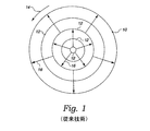
今日最も広く普及している乾燥技術は、スピンリンス乾燥(SRD)である。図1は、SRDによる乾燥処理の際の、ウエハ10上における洗浄液の動きを示している。この乾燥処理では、湿ったウエハが、回転14の方向に高速で回転される。流体の方向の矢印16によって示されるように、SRDでは、ウエハの洗浄に使用された水または洗浄液が、遠心力の作用によって、ウエハの中心から引き離れてウエハの外側に引っ張られ、最終的にはウエハから引きずり落とされる。洗浄液がウエハから引き離されるにつれて、ウエハの中心には、液体と気体との移動境界面12が形成される。この境界面は、乾燥処理の進行に伴って、ウエハの外側に向かって移動する(すなわち、液体と気体との移動境界面12によって生成される円が大きくなる)。図1の例では、液体と気体との移動境界面12によって形成される円の内側は液体が無く、液体と気体との移動境界面12によって形成される円の外側は洗浄液である。したがって、乾燥処理の続行に伴って、液体と気体との移動境界面12の内側の領域(乾燥領域)は増大し、液体と気体との移動境界面12の外側の領域(濡れ領域)は減少する。先述のように、もし液体と気体との移動境界面12が壊れた場合には、ウエハ上に洗浄液の液滴が形成され、液滴の蒸発による汚染が引き起こされる。したがって、ウエハ表面上の汚染を回避するためには、液滴の形成およびそれに続く蒸発を制限することが肝要である。あいにく、今日の乾燥方法は、液体との移動境界面の崩壊を阻止することに関し、部分的に成功しているに過ぎない。
The most widespread drying technique today is spin rinse drying (SRD). FIG. 1 shows the movement of the cleaning liquid on the
また、SRD処理は、疎水性のウエハ表面を乾燥させることを得意としない。疎水性のウエハ表面の乾燥が難しいのは、このような表面が、水および水をベースにした(すなわち水性の)洗浄液をはじくからである。したがって、乾燥処理が続行され、洗浄液がウエハ表面から引き離されるのに伴って、残りの洗浄液は、(もし水性ならば)ウエハ表面によってはじかれる。その結果、水性の洗浄液は、疎水性のウエハ表面との接触領域を最小量にしようとする。また、水性の洗浄液は、表面張力を受けて(すなわち水素間分子結合を受けて)凝集する傾向がある。したがって、疎水性のウエハ表面上には、疎水性の相互作用および表面張力が原因で、水性洗浄液の玉(すなわち液滴)が制御不能な状態で形成される。このような液滴の形成は、前述のように、有害な蒸発および汚染を引き起こす。SRDに伴うこれらの制約は、液滴に作用する遠心力が最も小さいウエハの中心で、特に深刻である。したがって、SRD処理は、現段階で最もよく使用されているウエハ乾燥法であるにもかかわらず、特に疎水性のウエハ表面に適用される場合などに、ウエハ表面上で洗浄液の液滴の形成を低減させるのが困難である。 Also, the SRD process is not good at drying hydrophobic wafer surfaces. Hydrophobic wafer surfaces are difficult to dry because such surfaces repel water and water-based (ie, aqueous) cleaning solutions. Thus, as the drying process continues and the cleaning liquid is pulled away from the wafer surface, the remaining cleaning liquid is repelled by the wafer surface (if it is aqueous). As a result, the aqueous cleaning solution attempts to minimize the contact area with the hydrophobic wafer surface. In addition, the aqueous cleaning liquid tends to agglomerate under surface tension (i.e., under hydrogen molecular bonds). Therefore, on the surface of the hydrophobic wafer, due to the hydrophobic interaction and surface tension, an aqueous cleaning liquid ball (ie, a droplet) is formed in an uncontrollable state. The formation of such droplets causes harmful evaporation and contamination as described above. These limitations associated with SRD are particularly acute at the center of the wafer where the centrifugal force acting on the droplet is the smallest. Therefore, although the SRD process is the most commonly used wafer drying method at the present stage, the formation of droplets of the cleaning liquid on the wafer surface, particularly when applied to a hydrophobic wafer surface, is performed. It is difficult to reduce.
また、洗浄、エッチング、およびメッキなどの他のウエハ処理工程でも、やはり、ウエハへの流体の供給およびウエハからの流体の除去を、汚染を低減させると共にウエハの歩留まりを向上させる効果的な方法で行うにあたって問題がある。 Also in other wafer processing steps such as cleaning, etching, and plating, again, supplying and removing fluid from the wafer is an effective way to reduce contamination and improve wafer yield. There is a problem in doing.
したがって、従来技術に伴う問題を回避するための方法および装置であって、流体の管理およびそのウエハへの供給を最適化することによって、ウエハ表面上において汚染物の堆積を低減させることができる、方法および装置が必要とされている。今日頻繁に生じるこのような汚染物の堆積は、合格ウエハの歩留まりを低下させると共に、半導体ウエハの製造費用を増大させる。 Thus, a method and apparatus for avoiding the problems associated with the prior art, which can reduce the deposition of contaminants on the wafer surface by optimizing fluid management and supply to the wafer. What is needed is a method and apparatus. The deposition of such contaminants that occurs frequently today reduces the yield of acceptable wafers and increases the cost of manufacturing semiconductor wafers.
本発明は、概して、ウエハの汚染を低減させると同時にウエハ表面上において流体を管理することができる基板処理(例えば乾燥、洗浄、エッチング、およびメッキなど)装置を提供することによって、これらのニーズを満たすものである。本発明は、言うまでもなく、工程、装置、システム、デバイス、または方法を含む各種の形態で実現することができる。以下では、本発明のいくつかの実施形態が説明される。 The present invention generally addresses these needs by providing a substrate processing (e.g., drying, cleaning, etching, and plating) apparatus that can reduce wafer contamination while simultaneously managing fluid on the wafer surface. To meet. Needless to say, the present invention can be realized in various forms including a process, an apparatus, a system, a device, or a method. In the following, several embodiments of the invention will be described.
一実施形態において、基板をその基板の表面に供給される流体メニスカスで処理するための装置であって、基板の端部に隣接して基板と同一平面内に配置されるように構成されるドッキング表面を備える装置が提供される。該ドッキング表面は、流体メニスカスが基板の表面に出入りするのを可能にするための移動境界面を提供する。 In one embodiment, an apparatus for processing a substrate with a fluid meniscus supplied to the surface of the substrate, the docking configured to be disposed in the same plane as the substrate adjacent to an edge of the substrate. An apparatus comprising a surface is provided. The docking surface provides a moving interface to allow the fluid meniscus to enter and exit the surface of the substrate.
別の一実施形態において、基板の処理に使用するための装置であって、近接ヘッドのためのドッキングステーションを基板の端部に隣接する位置に保持するように構成されるクーポンマガジンを備える装置が提供される。 In another embodiment, an apparatus for use in processing a substrate comprising a coupon magazine configured to hold a docking station for a proximity head in a position adjacent to an end of the substrate. Provided.
別の一実施形態において、基板を処理するための方法であって、基板表面とほぼ共平面上に基板の端部に隣接して移動境界面を配置する工程を備える方法が提供される。該方法は、更に、移動境界面と基板表面との間で流体メニスカスを移動させる工程を備える。 In another embodiment, a method is provided for processing a substrate, the method comprising positioning a moving interface adjacent to an edge of the substrate substantially coplanar with the substrate surface. The method further comprises moving the fluid meniscus between the moving interface and the substrate surface.
本発明は、多数の長所を有する。最も顕著な長所は、本明細書で提示される装置および方法が、ウエハ表面上に残留する望ましくない流体および汚染物を低減させると同時に半導体ウエハを効率良く処理する(洗浄する、乾燥する、エッチングする、メッキする、ならびにウエハに対する流体の供給および流体の除去の少なくとも一方の最適管理を伴うその他の適切なウエハ処理を行う)という点にある。こうして、ウエハ処理が効率良く行われる結果、ウエハの処理および製造が拡大され、高いウエハ歩留まりが実現される。 The present invention has a number of advantages. The most notable advantage is that the apparatus and method presented herein efficiently treats semiconductor wafers (clean, dry, etch) while reducing undesirable fluids and contaminants remaining on the wafer surface. , Plating, and other suitable wafer processing with optimal management of at least one of fluid supply and fluid removal to the wafer). As a result of the efficient wafer processing, wafer processing and manufacturing are expanded and high wafer yield is achieved.
本発明は、マルチモジュールマニホルドの利用を通じて供給される処理液のインプットに併せて真空による流体の除去を行うことによって、改善された処理を可能にすることができる。マルチモジュールマニホルドは、一つまたはそれ以上のマニホルド部分の入れ替えを通じて、多数の形態のうちの任意の一形態に構成することができる。 The present invention can enable improved processing by removing the fluid by vacuum in conjunction with the input of processing liquid supplied through the use of a multi-module manifold. The multi-module manifold can be configured in any one of a number of forms through replacement of one or more manifold portions.
前述の力によってウエハ表面上の流体膜に作用する圧力は、他の処理技術と比べて汚染物の残留を大幅に低減させた状態で、ウエハ表面における流体の供給および除去の少なくとも一方を最適化することができる。また、本発明では、ウエハ表面の近くに真空を形成するのとほぼ平行して、ウエハ表面に向けてイソプロピルアルコール(IPA)蒸気および処理液を供給しても良い。これは、メニスカスの高度な生成および制御ならびに処理液の境界面に沿ったその表面張力の低減をいずれも可能にするので、汚染物を残留させることなしに、ウエハ表面に対する流体の供給および除去の少なくとも一方を最適化することができる。IPAおよび処理液のインプット、ならびに流体のアウトプットによって生成されたメニスカスは、ウエハを処理するために、ウエハ表面に沿って移動されて良い。 The pressure acting on the fluid film on the wafer surface due to the aforementioned forces optimizes at least one of the supply and removal of fluid on the wafer surface with significantly reduced contaminant residue compared to other processing techniques. can do. In the present invention, isopropyl alcohol (IPA) vapor and processing liquid may be supplied toward the wafer surface substantially in parallel with forming a vacuum near the wafer surface. This allows both high-level meniscus generation and control and reduction of its surface tension along the process liquid interface, so fluid supply and removal to the wafer surface without leaving contaminants. At least one of them can be optimized. The meniscus generated by the IPA and processing liquid inputs, and the fluid output may be moved along the wafer surface to process the wafer.
一実施形態では、ドッキングステーションを効果的に保持および配置するために、クーポンマガジンを使用することができる。ドッキングステーション(クーポンとしても知られる)は、ウエハ表面を模倣することができるので、近接ヘッドによって生成された流体メニスカスがウエハ表面上から離れる(またはウエハ表面上に達する)際に、ドッキングステーションは、メニスカスが通るためのほぼ連続した表面を提供し、そうして、メニスカスの安定性を強化することができる。また、処理されるウエハとほぼ共平面上にドッキングステーションがくるように、クーポンマガジンの高さを調整することができる。したがって、クーポンマガジンは、流体メニスカスを使用する任意の適切なウエハ処理工程に用いることができる。ウエハ処理は、このようにして、高度に強化および最適化することができる。 In one embodiment, a coupon magazine can be used to effectively hold and position the docking station. A docking station (also known as a coupon) can mimic the wafer surface, so that when the fluid meniscus generated by the proximity head moves away from (or reaches) the wafer surface, A substantially continuous surface for the meniscus to pass through can be provided, thus enhancing the meniscus stability. Also, the height of the coupon magazine can be adjusted so that the docking station is substantially coplanar with the wafer being processed. Thus, the coupon magazine can be used in any suitable wafer processing process that uses a fluid meniscus. Wafer processing can thus be highly enhanced and optimized.
本発明の原理を例示した添付の図面に併せて行われる以下の詳細な説明から、本発明の他の形態および長所が明らかになる。 Other aspects and advantages of the present invention will become apparent from the following detailed description, taken in conjunction with the accompanying drawings, illustrating by way of example the principles of the invention.
本発明は、添付の図面に併せて行われる以下の詳細な説明によって、容易に理解されるであろう。説明を容易にするため、類似の参照番号は類似の構成要素を表すものとする。 The present invention will be readily understood by the following detailed description in conjunction with the accompanying drawings. For ease of explanation, like reference numerals represent like components.
基板を処理するための方法および装置の発明が開示される。以下の説明では、本発明の完全な理解を促す目的で、数多くの詳細が設定されている。しかしながら、当業者ならば明らかなように、本発明は、これらの詳細の一部または全部が特定されなくても実施することができる。また、本発明が不必要に不明瞭にならないように、周知の処理工程の詳細な説明は省略されている。 An invention of a method and apparatus for processing a substrate is disclosed. In the following description, numerous details are set forth in order to facilitate a thorough understanding of the present invention. However, it will be apparent to those skilled in the art that the present invention may be practiced without some or all of these details being specified. In other instances, well known process operations have not been described in detail in order not to unnecessarily obscure the present invention.
本発明は、いくつかの好ましい実施形態の観点から説明されるが、当業者ならば、これまでの明細書を熟読し且つ図面を検討することによって、各種の代替、追加、置換、および等価物の形態を想到できることは、言うまでもない。したがって、本発明は、本発明の真の趣旨および範囲の範囲内において、このようなあらゆる代替、追加、置換、および等価物の形態を含むものと解釈される。 While the present invention is described in terms of several preferred embodiments, those skilled in the art will recognize various alternatives, additions, substitutions, and equivalents upon reading the previous specification and reviewing the drawings. It goes without saying that this form can be conceived. Accordingly, the present invention is to be construed as including all such alternatives, additions, substitutions and equivalents within the true spirit and scope of the present invention.
以下の図面は、流体メニスカスを特定の形状、大きさ、および位置に生成するための近接ヘッドを伴った、代表的なウエハ処理システムの実施形態を示している。一実施形態において、ここで用いられる技術は、メニスカス真空IPA蒸気(MVIV)技術として知られている。この技術は、例えばメニスカス真空IPA蒸気乾燥(MVIVD)、メニスカス真空IPA蒸気洗浄(MVIVC)、メニスカス真空IPA蒸気エッチング(MVIVE)、およびメニスカス真空IPA蒸気メッキ(MVIVP)などの任意の適切なウエハ工程を実施するために用いることができる。なお、このシステムは例示的なものであるので、近接ヘッドをウエハのごく近くに移動させることができる他の任意の構成が用いられても良いことは、言うまでもない。図示された実施形態において、近接ヘッドは、ウエハの中心部からウエハの端部へと直線移動することができる。なお、ウエハの端部からその対角線上にあるもうもう一方の端部へと近接ヘッドが直線移動する他の実施形態、または、例えば放射運動、円運動、螺旋運動、ジグザグ運動、もしくはランダム運動などの他の非直線的な移動形態が用いられても良いことは、言うまでもない。あるいは、ユーザの望みどおりに定められた任意の適切な運動プロファイルが用いられても良い。また、一実施形態では、ウエハを回転させると同時に近接ヘッドを直線移動させることができるので、近接ヘッドは、ウエハのあらゆる部分を処理することが可能になる。また、ウエハを回転させず、近接ヘッドをウエハのあらゆる部分を処理可能な方式でウエハ上を移動させる、他の実施形態を用いても良い。また、本明細書で提示される近接ヘッドおよびウエハ処理システムは、例えば200mmのウエハ、300mmのウエハ、およびフラットパネルなど、形状および大きさが任意である基板の処理に用いることができる。処理システムを、そのシステム構成に応じて、任意の適切なウエハ処理(例えばメッキ、エッチング、洗浄、および乾燥など)に用いられるように構成することができる。 The following drawings illustrate an exemplary wafer processing system embodiment with a proximity head for generating a fluid meniscus in a particular shape, size, and position. In one embodiment, the technique used here is known as the meniscus vacuum IPA vapor (MVIV) technique. This technique involves any suitable wafer process such as meniscus vacuum IPA vapor drying (MVIVD), meniscus vacuum IPA vapor cleaning (MVIVC), meniscus vacuum IPA vapor etching (MVIVE), and meniscus vacuum IPA vapor plating (MVIVP). Can be used to implement. Note that this system is exemplary, and it will be appreciated that any other configuration that can move the proximity head very close to the wafer may be used. In the illustrated embodiment, the proximity head can move linearly from the center of the wafer to the edge of the wafer. Other embodiments in which the proximity head moves linearly from one end of the wafer to the other end on the diagonal, or for example, radial motion, circular motion, spiral motion, zigzag motion, or random motion Of course, other non-linear movement modes may be used. Alternatively, any suitable exercise profile defined as desired by the user may be used. In one embodiment, the proximity head can be linearly moved simultaneously with the rotation of the wafer, allowing the proximity head to process any part of the wafer. Also, other embodiments may be used in which the proximity head is moved on the wafer in such a manner that any part of the wafer can be processed without rotating the wafer. Further, the proximity head and wafer processing system presented in this specification can be used for processing a substrate having an arbitrary shape and size, such as a 200 mm wafer, a 300 mm wafer, and a flat panel. The processing system can be configured to be used for any suitable wafer processing (eg, plating, etching, cleaning, drying, etc.) depending on the system configuration.
流体メニスカスは、近接ヘッドで支えると共に近接ヘッドで移動させる(例えばウエハ上に到達させる、ウエハ上から離れさせる、およびウエハ上を横切らせる)ことができる。本明細書で提示されるように、クーポンマガジンは、ドッキングステーションの保持および配置を行うことができるので、ドッキングステーションは、ウエハの端部から離れて位置することができ、そのうえ、流体メニスカスがウエハ上から離れる(またはウエハ上に到達する)際にウエハ表面を模倣することができる。したがって、ドッキングステーション(クーポンとしても知られる)は、メニスカスが通るためのほぼ連続した表面を提供し、そうすることによって、メニスカスの安定性を高めることができる。クーポンマガジンは、また、処理されているウエハとほぼ同じ高さ(すなわち共平面上)にドッキングステーションがくるように、ドッキングステーションの高さ調整を行うように構成されても良い。ドッキングステーションをウエハとほぼ共平面上に持ってくることによって、流体メニスカスをウエハ上に到達させ(またはウエハ上から離れさせ)、メニスカスの安定性を維持することができる。 The fluid meniscus can be supported by the proximity head and moved by the proximity head (e.g., reaching the wafer, moving away from the wafer, and traversing the wafer). As presented herein, the coupon magazine can hold and place the docking station so that the docking station can be located away from the edge of the wafer, and the fluid meniscus is located on the wafer. The wafer surface can be imitated as it leaves the top (or reaches the wafer). Thus, a docking station (also known as a coupon) provides a substantially continuous surface for the meniscus to pass through, thereby increasing the meniscus stability. The coupon magazine may also be configured to adjust the height of the docking station so that the docking station is at approximately the same height (ie, coplanar) as the wafer being processed. By bringing the docking station substantially coplanar with the wafer, the fluid meniscus can reach (or move away from) the wafer and maintain meniscus stability.
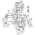
図2Aは、本発明の一実施形態におけるウエハ処理システム100を示している。システム100は、ウエハ表面の処理を可能にするためにウエハの保持および回転の少なくとも一方を行うローラ102a,102bを備える。システム100は、また、一実施形態においてそれぞれ上部アーム104aおよび下部アーム104bに取り付けられている近接ヘッド106a,106bを備える。近接ヘッドは、流体メニスカスの生成を可能にする任意の適切な装置であっても良い。上部アーム104aおよび下部アーム104bは、ウエハの半径に沿った、近接ヘッド106a,106bのほぼ直線的な移動を可能にするアセンブリにおいて、その一部を構成することができる。更に別の一実施形態において、該アセンブリは、ユーザによって定められた任意の適切な動きで近接ヘッド106a,106bを移動させても良い。
FIG. 2A illustrates a wafer processing system 100 in one embodiment of the present invention. The system 100 includes rollers 102a and 102b that perform at least one of holding and rotating the wafer to enable processing of the wafer surface. The system 100 also includes
一実施形態において、アーム104は、近接ヘッド106aおよび近接ヘッド106bを、それぞれウエハの上方および下方に且つウエハのごく近くに保持するように構成される。例えば、代表的な一実施形態において、これは、近接ヘッドが水平に移動してウエハ処理の開始位置に到達した時点で、近接ヘッド106a,106bが垂直に移動してウエハのごく近くに到達することができるように、上部アーム104aおよび下部アーム104bを垂直に移動可能にすることによって、実現されても良い。別の一実施形態において、上部アーム104aおよび下部アーム104bは、処理に先立ってメニスカスが生成され、尚かつ近接ヘッド106a,106bの間で生成されたそのメニスカスが処理対象のウエハ108の端部領域からそのウエハ表面上に到達する一位置において、近接ヘッド106a,106bをスタートさせるように構成されても良い。したがって、上部アーム104aおよび下部アーム104bを、本明細書で提示されるウエハ処理を可能にする方式で近接ヘッド106a,106bを移動させることができる任意の適切な形態に構成することができる。当然のことながら、システム100は、近接ヘッドをウエハのごく近くに移動させることによって、メニスカスの生成および制御を行うことができる限り、任意の適切な形態に構成されても良い。なお、ごく近くとは、メニスカスを維持できる限り、ウエハから任意の適切な距離であれば良い。一実施形態において、近接ヘッド106a,106b(および本明細書で提示される他の任意の近接ヘッド)のそれぞれを、ウエハ表面上に流体メニスカスを生成するために、ウエハから約0.1mm〜約10mmの位置に配することができる。好ましい一実施形態において、近接ヘッド106a,106b(および本明細書で提示される他の任意の近接ヘッド)のそれぞれは、ウエハ表面上に流体メニスカスを生成するために、ウエハから約0.5mm〜約2.0mmの位置に配され、更に好ましい一実施形態において、近接ヘッド106a,106b(および本明細書で提示される他の任意の近接ヘッド)のそれぞれは、ウエハ表面上に流体メニスカスを生成するために、ウエハから約1.50mmの位置に配される。
In one embodiment,
一実施形態において、システム100のアーム104は、ウエハの処理済み部分から未処理部分へと近接ヘッド106a,106bを移動させることができるように構成される。当然のことながら、これらのアーム104は、望みどおりのウエハ処理を可能にする方式で、近接ヘッド106a,106bを移動させることができる任意の適切な方式で移動可能であれば良い。一実施形態において、ウエハの表面に沿った近接ヘッド106a,106bを動かすために、これらのアーム104をモータによって駆動しても良い。なお、図中のウエハ処理システム100は、近接ヘッド106a,106bを伴っているが、例えば1つ、2つ、3つ、4つ、5つ、6つなど、任意の適切な数の近接ヘッドが用いられても良いことは、言うまでもない。また、ウエハ処理システム100の近接ヘッド106a,106bの少なくとも一方は、例えば本明細書で提示される任意の近接ヘッドによって示されるように、任意の適切な大きさまたは形状にすることができる。本明細書で提示されるこれらの各種の構成は、近接ヘッドとウエハとの間で流体メニスカスを生成する。流体メニスカスは、ウエハ表面に対して流体を供給すると共にその表面から流体を除去することによって、ウエハを横切るように移動して、ウエハを処理することができる。このように、ウエハに供給される流体に応じて、洗浄、乾燥、エッチング、およびメッキの少なくとも一つを実現することができる。したがって、近接ヘッド106a,106bは、本明細書で提示される多数の構成のうちの任意の構成をとることもできるし、あるいは、本明細書で提示される処理を可能にするその他の構成をとることもできる。当然のことながら、システム100は、ウエハの片面を処理しても良いし、あるいは、ウエハの上面および下面の両方を処理しても良い。
In one embodiment, the
また、ウエハの上面および下面の少なくとも一方を処理する以外に、システム100は、異なる種類の流体を出し入れすることによって、あるいは、異なる構成のメニスカスを使用することによって、ウエハの片面に一処理を施す一方で、ウエハのもう片面には同じ処理または異なる処理を施すように、構成されても良い。近接ヘッドは、また、ウエハの上面および下面の少なくとも一方に加えて、ウエハの斜めの端部も処理するように、構成することができる。これは、斜めの端部を処理するメニスカスをウエハの端部上に到達させる(または端部上から離れさせる)ことによって、実現することができる。当然のことながら、近接ヘッド106a,106bは、同じ種類の装置であっても良いし、あるいは、互いに異なる種類の近接ヘッドであっても良い。 In addition to processing at least one of the upper and lower surfaces of the wafer, the system 100 performs one process on one side of the wafer by moving in and out of different types of fluids or by using differently configured meniscuses. On the other hand, the other side of the wafer may be configured to perform the same process or different processes. The proximity head can also be configured to process an oblique edge of the wafer in addition to at least one of the upper and lower surfaces of the wafer. This can be achieved by having the meniscus that processes the oblique edges reach (or move away from) the wafer edges. As a matter of course, the proximity heads 106a and 106b may be the same type of apparatus, or may be different types of proximity heads.
ウエハ108は、その処理される領域のごく近くに所望の近接ヘッドを持ってくることができる任意の適切な向きで、ローラ102a,102bによって保持および回転されても良い。一実施形態において、ローラ102a,102bは、時計回りに回転することによって、ウエハ108を反時計回りに回転させることができる。なお、これらのローラは、所望されるウエハの回転に応じて、時計回りまたは反時計回りのいずれに回転されても良い。一実施形態において、ローラ102a,102bによってウエハ108に付与される回転は、ウエハの未処理領域を近接ヘッド106a,106bのごく近くに移動させる働きをする。しかしながら、回転そのものは、ウエハを乾燥させることも、ウエハ表面上の流体をウエハの端部に向けて移動させることもない。したがって、代表的な一ウエハ処理工程において、ウエハの未処理領域は、近接ヘッド106a,106bの直線運動およびウエハ108の回転運動の両方を通じて近接ヘッド106a,106bに供される。ウエハ処理工程そのものは、少なくとも一つの近接ヘッドによって実行することができる。したがって、一実施形態において、ウエハ108の処理済み部分は、処理工程が進行するにつれてウエハ108の中心領域から端領域へと螺旋運動の形で拡大してゆく。別の一実施形態において、ウエハ108の処理済み部分は、近接ヘッド106a,106bがウエハ108の縁からウエハ108の中心へと移動するにつれてウエハ108の端領域からウエハ108の中心領域へと螺旋運動の形で拡大してゆく。
代表的な一実施形態において、近接ヘッド106a,106bは、ウエハ108の乾燥、洗浄、エッチング、およびメッキの少なくとも一つの処理を行うように構成されても良い。代表的な乾燥の一実施形態において、少なくとも一つの第1の供給口は、脱イオン水(DIW)をインプットするように構成されて良く(DIW供給口としても知られる)、少なくとも一つの第2の供給口は、イソプロピルアルコール(IPA)の蒸気を含有するN2キャリアガスをインプットするように構成されても良く(IPA供給口としても知られる)、少なくとも一つの排出口は、真空にすることによってウエハと特定の近接ヘッドとの間の領域から流体を除去するように構成されても良い(真空排出口としても知られる)。いくつかの代表的な実施形態では、IPA蒸気が使用されているが、例えば窒素、任意の適切なアルコール蒸気、有機化合物、および揮発性化学剤など、水に対して混和性の他の任意の蒸気が用いられても良い。なお、任意の適切なアルコール蒸気は、任意の適切なアルコールを含んで良い。そして、任意の適切なアルコールは、飽和炭素原子に付いた水酸基を伴う炭素ベースの任意の適切な化学剤であって良い。
In an exemplary embodiment, the proximity heads 106a, 106b may be configured to perform at least one of drying, cleaning, etching, and plating of the
代表的な洗浄の一実施形態では、DIWが洗浄液に置き換えられて良い。代表的なエッチングの一実施形態では、DIWをエッチャントで置き換えた状態でエッチングを実施することができる。更なる一実施形態では、処理液を伴う流体メニスカスおよびメッキ用に構成された近接ヘッドによって、メッキをおこなうことができる。また、所望される処理工程に応じ、第1の供給口および第2の供給口に他の溶液がインプットされても良い。 In an exemplary cleaning embodiment, DIW may be replaced with a cleaning solution. In an exemplary etch embodiment, the etch can be performed with DIW replaced with an etchant. In a further embodiment, the plating can be performed by a fluid meniscus with processing liquid and a proximity head configured for plating. Further, another solution may be input to the first supply port and the second supply port according to a desired processing step.
近接ヘッドの面上に設けられた供給口および排出口は、本明細書で提示された安定したメニスカスを利用可能である限り、任意の適切な構成であれば良い。一実施形態では、少なくとも一つのN2/IPA蒸気供給口を少なくとも一つの真空排出口に隣接して設け、この少なくとも一つの真空排出口を更に少なくとも一つの処理液供給口に隣接して設けることによって、IPA−真空−処理液の配位を設定することができる。なお、所望のウエハ処理および強化を図りたいウエハ処理機能の種類に応じ、例えばIPA−処理液−真空、処理液−真空−IPA、および真空−IPA−処理液などの他の配位が用いられても良い。好ましい一実施形態では、ウエハを処理する目的で、近接ヘッドとウエハとの間で高度に且つ強力にメニスカスの生成、制御、および移動を行うために、IPA−真空−処理液の配位を用いることができる。処理液供給口、N2/IPA蒸気供給口、および真空排出口は、上述された配位が維持される限り、適切な任意の形で配置されて良い。例えば、追加の一実施形態では、所望の近接ヘッドの構成に応じ、上記のN2/IPA蒸気供給口、真空排出口、および処理液供給口に加えてIPA蒸気排出口、処理液供給口、および真空排出口の少なくとも一つが追加で設けられても良い。なお、IPA−真空−処理液の配位の厳密な構成は、利用形態に応じて可変である。例えば、IPA供給口の位置と、真空の位置と、処理液供給口の位置との間の距離は、これらの距離が一致するように、あるいはこれらの距離が一致しないように変更されても良い。また、IPA供給口と、真空と、処理液排出口との間の距離は、近接ヘッド106aの大きさ、形状、および構成、ならびに処理メニスカスの所望の大きさ(すなわちメニスカスの形状および大きさ)に応じて大きさが異なっても良い。また、代表的なIPA−真空−処理液の配位は、参照のために前掲された方法で求めることができる。
The supply port and the discharge port provided on the surface of the proximity head may have any appropriate configuration as long as the stable meniscus presented in this specification can be used. In one embodiment, at least one N 2 / IPA vapor supply port is provided adjacent to at least one vacuum discharge port, and the at least one vacuum discharge port is further provided adjacent to at least one processing liquid supply port. Can set the coordination of the IPA-vacuum-treatment liquid. Depending on the type of wafer processing function desired to be processed and enhanced, other configurations such as IPA-processing liquid-vacuum, processing liquid-vacuum-IPA, and vacuum-IPA-processing liquid are used. May be. In a preferred embodiment, the IPA-vacuum-treatment liquid configuration is used for highly and powerful meniscus generation, control, and movement between the proximity head and the wafer for wafer processing purposes. be able to. The treatment liquid supply port, the N 2 / IPA vapor supply port, and the vacuum discharge port may be arranged in any appropriate form as long as the above-described coordination is maintained. For example, in an additional embodiment, depending on the desired configuration of the proximity head, in addition to the N 2 / IPA vapor supply port, the vacuum discharge port, and the treatment liquid supply port, an IPA vapor discharge port, a treatment liquid supply port, In addition, at least one of the vacuum outlets may be additionally provided. The exact configuration of the IPA-vacuum-treatment liquid coordination is variable depending on the usage. For example, the distance between the position of the IPA supply port, the position of the vacuum, and the position of the processing liquid supply port may be changed so that these distances match or these distances do not match. . The distance between the IPA supply port, the vacuum, and the processing liquid discharge port is the size, shape, and configuration of the
一実施形態において、近接ヘッド106a,106bは、ウエハ108の上面および下面のごく近くにそれぞれ配置されても良く、更に、IPA供給口、DIW供給口、および1つまたはそれ以上の真空排出口を用いて、ウエハ108の上面および下面を処理することができるウエハ処理用のメニスカスをウエハ108に接触するように生成しても良い。ウエハ処理用のメニスカスは、前掲の利用形態を参照して行われた説明にしたがって生成することができる。IPAおよび処理液のインプットとほぼ同時に、ウエハ表面のごく近くには、IPA蒸気、処理液、およびウエハ表面上に存在し得る流体の少なくとも一つを除去するための真空が形成されても良い。代表的な本実施形態では、IPA蒸気が使用されているが、例えば窒素、適切な任意のアルコール蒸気、有機化合物、ヘキサノール、エチルグリコール、およびアセトンなど、水に対して混和性の他の任意の蒸気が用いられても良い。これらの流体は、表面張力を低減させる流体としても知られている。メニスカスは、近接ヘッドとウエハとの間の領域にある部分の処理液である。なお、本明細書で使用される「アウトプット」は、ウエハ108と特定の近接ヘッドとの間の領域から流体を除去することを意味するものとし、「インプット」は、ウエハ108と特定の近接ヘッドとの間の領域に流体を導入することを意味するものとする。
In one embodiment, the proximity heads 106a, 106b may be located very close to the top and bottom surfaces of the
流体メニスカスは、ウエハ108の端部からウエハ上に到達することができる(またはウエハ108の端部からウエハを離れることができる)。ウエハ108の縁部において流体メニスカスの除去および供給の少なくとも一方を行うために、システム100は、その一実施形態において、ウエハ処理アセンブリの上面に取り付けられたカップルマガジン126を備える。一実施形態において、クーポンアセンブリ126は、下部124と上部122とを有する。クーポンアセンブリ126は、ドッキングステーション120を、ウエハ平面に対してほぼ平面的であると共に近接ヘッド106aと近接ヘッド106bとの間である正確な固定位置に保持するように構成されても良い。好ましい一実施形態において、ドッキングステーション120がウエハ面とほぼ共平面上にない場合は、ドッキングステーション120は、ウエハ108がドッキングステーションとほぼ共平面上にくるように、(図7を参照にして詳述されるように)レベリング機構を用いて調整することができる。したがって、ドッキングステーションは、図2Bを参照にして詳述されるように、近接ヘッド106によって実行されている処理が終了し且つウエハ表面から離れる際に、ウエハ表面を模倣することができる。なお、本明細書で提示されるドッキングステーション120は、言うまでもなく、石英またはセラミックなどの適切な任意の親水性材料で形成されても良い。ドッキングステーションは、基板と同一平面内において基板の端部に隣接する流体メニスカス用ドッキング表面を有しても良い。ドッキングステーションのドッキング表面は、流体メニスカスが基板表面に出入りすることを可能にする移動境界面を形成することができる。一実施形態において、ドッキング表面は、基板の外周形状に合致する外周形状を有する。その結果、ドッキング表面は、近接ヘッドの流体メニスカスのための移動境界面を形成することができる。したがって、ウエハを模倣したほぼ連続的な表面を提供することによって、ウエハ108に到達するまたはウエハ108から離れるメニスカスを安定した状態に保つことができる。
The fluid meniscus can reach the wafer from the edge of the wafer 108 (or can leave the wafer from the edge of the wafer 108). To perform fluid meniscus removal and / or delivery at the edge of the
なお、マガジンクーポン126は、近接ヘッドの技術を用いるにあたって、規則的なまたは不規則的な幾何学的形状の基板を処理用の固定位置にしっかりと保持し且つ高さ調整するという、具体的な意図をもって設計されても良い。また、マガジンクーポン126は、例えばエッチング、洗浄、乾燥、およびメッキなど、近接ヘッドによって行われる任意の適切な工程に用いられても良い。
It should be noted that the
一実施形態において、クーポンマガジン126は、クーポンマウント128に取り付けられる。一実施形態において、クーポンマガジン126およびクーポンマウント128は、クーポンマガジンアセンブリとも呼ぶことができる。
In one embodiment,
図2Bは、本発明の一実施形態におけるドッキングステーション120を使用する代表的な近接ヘッドドッキング工程を示している。ドッキングステーション120は、ウエハ108上で形成されたメニスカスを崩壊させることなくドッキングステーション102へと移動させられるように、弧状の湾曲108aを模倣することができる表面120aを有していても良い。代表的な一実施形態において、近接ヘッド106は、ウエハ108の位置106から離れてドッキングステーション120上の位置へと移動することができる。ドッキングステーションは、クーポンマガジン122内の適所に保持される。
FIG. 2B illustrates an exemplary proximity head docking process using the
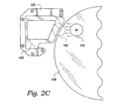
図2Cは、本発明の一実施形態におけるウエハ108から離れてドッキングステーション120へと移動するメニスカスを示している。代表的な一実施形態において、近接ヘッド106によって形成されたメニスカス140は、後述される利用形態において更に詳述されるように、ウエハ108のウエハ表面を処理するために用いられても良い。メニスカス140は、ウエハから位置160へと移動されても良い。位置160は、ウエハ108の表面を模倣するドッキングステーション120の一部を含む。なお、ドッキングステーション120は、ウエハ表面を模倣することによってメニスカス140を安定した状態に維持することができる任意の適切な形に構成されても良い。また、ドッキングステーションは、メニスカス140がウエハ108から離れる際にウエハ表面を効果的に模倣することができる任意の適切な距離だけウエハ108から離れていても良い。一実施形態において、ウエハに最も近い部分のドッキングステーション120は、ウエハから0.01〜10.0mmの距離にある。好ましい一実施形態において、ドッキングステーション120は、ウエハ108から約0.1mmの距離に位置する。
FIG. 2C illustrates the meniscus moving away from the
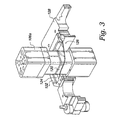
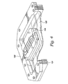
図3は、本発明の一実施形態におけるクーポンマガジン126を見やすくするためにいくつかの構成要素を省略して示したシステム100の拡大図である。クーポンマガジン126は、下部126に取り付けられた上部122を有しても良い。このような一実施形態において、上部122および下部126は、それらの間に位置するドッキングステーションの少なくとも一部に取り付けられることができる。一実施形態において、クーポンマガジン126は、例えばポリエチレンテレフタレート(PET)、ポリフッ化ビニリデン(PVDF)、およびポリエーテルエーテルケトン(PEEK)などの化学的に適合性で且つ機械的に安定な材料で作成されるデバイスホルダである。クーポンマガジン126は、所望の許容誤差の範囲内において、いくつかの正確な特徴を伴うように機械加工されても良い。クーポンマガジン126は、任意の適切な幾何学的大きさ、形状、および厚さを有する基板を、任意の適切な組み合わせの近接ヘッドの間、上方または下方に、確実に且つ正確に配置するように構成されても良い。本明細書で掲示される近接ヘッドは、MVIVマニホルドとしても知られている。クーポンマガジン126は、任意の適切な実験室検査用の取り付け備品または近接ヘッドを使用する任意の適切な製造装置において用いられても良い。ドッキングステーション120は、図7を参照にして説明されるように、カップルマガジン126の調整、すなわち高さ合わせによって、ウエハ表面に対してほぼ平面的にすることができる。一実施形態では、ドッキングステーション120をウエハ表面と共平面上にもってくるために、クーポンマガジン126およびクーポンマガジンマウント128のいずれか一方または両方が調整できる。したがって、クーポンマガジン126は、極めて柔軟な使用が可能であるうえ、ウエハ処理工程の高度に且つ強力に最適化することができる。
FIG. 3 is an enlarged view of the system 100 with some components omitted to facilitate viewing of the
図4は、本発明の一実施形態における近接ヘッド106の一部を伴うカップルマガジン126を詳細に示した図である。図中には、供給口および排出口が示されている。一実施形態において、クーポンアセンブリ126は、上部122および下部124の形状および大きさを変化させることによって、例えば200mmのドッキングステーションおよび300mmのドッキングステーションなどのように、任意の具体的形状のドッキングステーション120を保持するように構成されても良い。クーポンマガジン126は、また、任意のランダム形状を有する様々な大きさおよび厚さのウエハを保持しても良い。
FIG. 4 is a detailed view of the
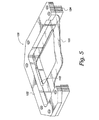
図5は、本発明の一実施形態における近接ヘッド106を伴わないクーポンマガジン126を示している。一実施形態において、クーポンマガジン126は、図2に代表的な形態を示されるような近接ヘッド106aおよび106bを機械的に且つ視覚的に検査するためのアクセスを可能にする覗き窓140を有する。このようにして、近接ヘッド106a,106bの移動量はもちろん、近接ヘッド106aと近接ヘッド106bとの間の距離も決定することができる。
FIG. 5 illustrates a
図6は、本発明の一実施形態におけるクーポンマガジン126の上面図を示している。図に示されたクーポンマガジン126は、上述の図2Aに示されるようにクーポンマガジン126をクーポンマガジンマウント128に止めるための取り付け穴320を含んでいても良い。なお、クーポンマガジン126をクーポンマガジンマウント128に取り付けるには、数、種類、および構成の少なくとも一つが任意の適切なものである取り付け穴320を用いることができる。別の一実施形態において、クーポンマガジン126は、取り付け穴320を使用せずに、接着によってクーポンマガジンマウントに取り付けられても良い。したがって、クーポンマガジン126は、各種のドッキングステーションを伴う各種のクーポンマガジンを手軽に且つ短時間で交換可能であるような方式で、クーポンマガジンマウント128からの取外しとクーポンマガジンマウント128への取付けができる。
FIG. 6 shows a top view of the
一実施形態において、ドッキングステーション120の外縁部分は、クーポンマガジン126の上部122と下部124との間に挟まれている。ドッキングステーション120は、このようにして、ウエハ処理工程の間、しっかりと保持される。図中のドッキングステーション120は、内部に開口部を有する形で示されているが、メニスカスの崩壊を生じることなく流体メニスカスをウエハからドッキングステーションへと(およびその逆方向へと)移動させることができる任意の適切な構成を有していても良い。図中のクーポンマガジン126は、長方形で示されているが、ドッキングステーション120がしっかりと保持され尚かつ近接ヘッドが妨害を受けることなくドッキングステーションに近づいたりドッキングステーションから離れたりすることができる限り、形状および構成の少なくとも一方が任意の適切なものにすることができる。別の一実施形態において、クーポンマガジンは、本明細書に提示される方法でドッキングステーション120が保持および配置される限り、例えば1,2,3,4,5などの任意の適切な数の要素を有していても良い。
In one embodiment, the outer edge portion of the
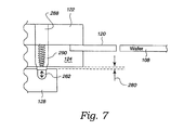
図7は、本発明の一実施形態におけるレベリング機構を示した図である。一実施形態において、レベリング機構は、ドッキングステーション120をウエハ108のほぼ共平面上に持ってこられるように、クーポンマガジンを垂直面内で移動させることができる。一実施形態において、クーポンマガジン126の上部122は、クーポンマガジンマウント128内のボール止め262を終端とするネジ290に通じるアクセスポート288を含んでいても良い。ネジ290は、バネを含んでいても良い。ボール止め262は、クーポンアセンブリマウント128に接していても良い。一実施形態において、バネ264は、約5〜15ポンド重の力を有していても良い。ネジ290を回転させることによって、ボール止め262は垂直に移動され、これは、クーポンマガジン126を、ひいてはドッキングステーション120を垂直に移動させる。したがって、クーポンマガジン126は、ドッキングステーション120をウエハ108とほぼ同じ高さにするように、垂直に移動することが可能である。一実施形態において、クーポンマガジン126は、距離280で示されるように垂直に移動することができる。なお、クーポンマガジン126を移動させることを目的とした図中の装置および方法は、代表的な性質のものであるので、クーポンマガジン126を移動させる方法として、任意の他の適切な形態が用いられても良いことは、言うまでもない。
FIG. 7 is a view showing a leveling mechanism in an embodiment of the present invention. In one embodiment, the leveling mechanism can move the coupon magazine in a vertical plane so that the
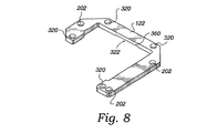
図8は、本発明の一実施形態におけるクーポンマガジン126の上部122を示している。上部122は、クーポンマガジンマウント128および下部124の両方に取り付けるために、数および種類の少なくとも一方が任意の適切なものである取り付け穴を含んでいても良い。一実施形態において、上部122は、上部122をクーポンマガジンマウント128に止め付けるための取り付け穴320を有していても良い。上部122は、また、上部122をクーポンマガジンマウント128に止め付けるために用いることができる取り付け穴202を有していても良い。上部122は、また、(下部124と組み合わされた際に)図5を参照にして上述された覗き窓を形成することができる窪み322を含んでも良い。
FIG. 8 shows the
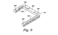
図9は、本発明の一実施形態におけるクーポンマガジン126の下部124を示している。下部124は、上部122の取り付け穴320に揃えることができる取り付け穴390を含んでいる。したがって、下部124は、取り付け穴390の使用によって上部122に止め付けられて、クーポンマガジン126を形成することができる。なお、上部122を下部124に繋げるために、例えば糊付けや接着などの任意の適切な取り付け方法が使用されても良いことは、言うまでもない。下部124は、やはり言うまでもなく、数および構成の少なくとも一方が任意の適切なものである取り付け穴390を有していても良い。
FIG. 9 shows the
下部124は、また、上部の窪み322と組み合わされた際に覗き窓140を形成することができる窪み380を有していても良い。近接ヘッド同士の位置関係およびドッキングステーション120に対する近接ヘッドの位置関係は、このように、視覚的および機械的の少なくとも一方の方法でアクセスすることができる。また、下部124は、下部124の内部の周囲をほぼ取り囲む凹所392を有していても良い。凹所392は、ドッキングステーション120の外周を収めることによって確実で且つ丁度良い取り付けを実現することができるように構成されても良い。以下では、流体メニスカスを生成することができる代表的な近接ヘッドに関して説明される。
The
以下の図面は、流体メニスカスを生成することができる代表的な近接ヘッドを伴う代表的なウエハ処理システムを示したものである。なお、本明細書で提示される本発明の実施形態において、流体メニスカスを生成することができる任意の適切な種類の近接ヘッドを伴う任意の適切な種類のシステムが使用されても良いことは、言うまでもない。 The following drawings illustrate an exemplary wafer processing system with an exemplary proximity head capable of generating a fluid meniscus. Note that in the embodiments of the invention presented herein, any suitable type of system with any suitable type of proximity head capable of generating a fluid meniscus may be used. Needless to say.
図10は、本発明の一実施形態におけるウエハ処理システム1100を示している。なお、例えばローラ、ピン、およびプラテンなど、ウエハを保持するまたは移動させる任意の適切な方法が使用可能であることは、言うまでもない。システム1100は、ウエハを保持するおよび回転させることによってウエハ表面の処理を可能にするローラ1102a,1102b,1102cを含んでいても良い。システム1100は、一実施形態において上部アーム1104aおよび下部アーム1104bにそれぞれ取り付けることができる近接ヘッド106a,106bを含んでいても良い。上部アーム1104aおよび下部アーム1104bは、ウエハの半径に沿った、近接ヘッド106a,106bのほぼ直線的な移動を可能にする近接ヘッドキャリアアセンブリ1104において、その一部を構成することができる。一実施形態において、近接ヘッドキャリアアセンブリ1104は、近接ヘッド106aおよび近接ヘッド106bを、それぞれウエハの上方および下方に且つウエハのごく近くに保持するように構成されても良い。これは、近接ヘッドが水平に移動してウエハ処理の開始位置に到達した時点で、近接ヘッド106a,106bが垂直に移動してウエハのごく近くに到達することができるように、上部アーム1104aおよび下部アーム1104bを垂直に移動可能にすることによって、実現することができる。別の一実施形態において、流体メニスカスは、二つの近接ヘッド104a,104bの間に形成され、ウエハの上面および下面に移動されても良い。上部アーム1104aおよび下部アーム1104bは、近接ヘッド106a,106bを移動させることによって、本明細書に提示されたウエハ処理を可能にする任意の適切な形で構成されても良い。なお、近接ヘッドをウエハのごく近くに移動させることによって、ウエハ表面上におけるメニスカスの生成および制御を可能にする限り、任意の適切な形でシステム1100を構成することができる。別の代表的な一実施形態において、近接ヘッド106は、アームの第2端によって定められる軸を中心に回転するアームの第1端に位置することができる。したがって、このような一実施形態では、近接ヘッドは、ウエハの表面の上方を弧状に移動することができる。更に別の一実施形態において、アームは、回転運動と直線運動とを組み合わせた形で移動することができる。図に示されたウエハは、各面に一つずつの近接ヘッドを有しているが、片面に一つの近接ヘッドを配されるだけでも良い。近接ヘッド106が使用されない面に対しては、ウエハスクラブブラシなどの他の表面調整処理を実施することができる。
FIG. 10 shows a
別の一実施形態において、システム1100は、ウエハに隣接する移動表面を有する近接ヘッドドッキングステーションを備えていても良い。このような一実施形態において、流体メニスカスは、制御され且つ管理された状態で、ドッキングステーションとウエハ表面との間を移動することができる。繰り返しになるが、もしウエハの片面のみで処理が必要とされる場合は、一つの近接ヘッドを伴う一本のアームのみが用いられても良い。
In another embodiment, the
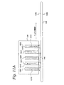
図11Aは、本発明の一実施形態におけるウエハ処理工程を実施する近接ヘッド106を示している。一実施形態において、近接ヘッド106は、ウエハ処理工程を実施するために、ウエハ108の上面108aのごく近くを移動する。なお、ウエハ108に供給される流体の種類に応じて、近接ヘッド106によってウエハ表面108a上に生成される流体メニスカス140が例えば洗浄、すすぎ、乾燥、エッチング、およびメッキなどの任意の適切なウエハ処理工程を行うことが好ましい。また、近接ヘッド106は、ウエハ108の下面108bを処理するために用いられても良い。一実施形態では、流体メニスカスが上面108aを処理しているあいだ、近接ヘッド106が移動可能であるように、ウエハ108が回転されても良い。別の一実施形態では、近接ヘッド106がウエハ表面上に流体メニスカスを生成しているあいだ、ウエハ108は静止した状態に維持されても良い。近接ヘッドは、次いで、ウエハ表面の上方を移動する、すなわちウエハ表面をスキャンすることによって、流体メニスカスをウエハの表面に沿って移動させても良い。別の一実施形態において、近接ヘッド106は、流体メニスカスがウエハの全表面に及ぶように、十分な大きさに作成されていれば良い。このような一実施形態では、ウエハの表面に流体メニスカスを供給することによって、近接ヘッドを動かすことなくウエハの全表面を処理することができる。
FIG. 11A shows a
一実施形態において、近接ヘッド106は、ソース供給口1302,1306およびソース排出口1304を含む。このような一実施形態では、窒素ガスに含有されるイソプロピルアルコール蒸気IPA/N21310がソース供給口1302を通じてウエハ表面に供給され、真空1312がソース排出口1304を通じてウエハ表面に供給され、処理液1314がソース供給口1306を通じてウエハ表面に供給される。
In one embodiment, the
一実施形態において、流体メニスカス140は、ウエハ表面108aから処理液1314およびIPA/N21310を除去するために真空1312を供給することに加えて、IPA/N21310および処理液1314を供給することによって、生成することができる。流体メニスカス140は、近接ヘッド106とウエハ表面との間に形成される流体層であり、安定した且つ制御可能な状態でウエハ表面108aを横切って移動することができる。一実施形態において、流体メニスカス140は、処理液1314の供給および除去をコンスタントに行うことによって形成されても良い。流体メニスカス140を形成する流体層は、ソース供給口1306、ソース排出口1304、およびソース供給口1302の大きさ、数、形状、およびパターンの少なくとも一つに応じ、形状および大きさの少なくとも一方が任意の適切なものとすることができる。
In one embodiment,
また、真空、IPA/N2、真空、および処理液の流量は、生成を所望される流体メニスカスの種類に応じ、任意の適切な値を用いることができる。更に別の一実施形態において、IPA/N2は、近接ヘッド106とウエハ表面との間の距離に応じ、流体メニスカス106の生成および使用の際に省略されても良い。このような一実施形態において、近接ヘッド106は、ソース供給口1312を備えていないので、流体メニスカス140は、ソース供給口1306による処理液1314の供給およびソース排出口1304による処理液1314の除去のみによって生成される。
In addition, the vacuum, IPA / N 2 , vacuum, and flow rate of the processing liquid can be any appropriate value depending on the type of fluid meniscus desired to be generated. In yet another embodiment, IPA / N 2 may be omitted during production and use of
近接ヘッド106の他の実施形態において、近接ヘッド106の処理表面(近接ヘッドのうちソース供給口およびソース排出口が位置する領域)は、生成される流体メニスカスの構成に応じ、任意の適切なトポグラフィを有していても良い。一実施形態において、近接ヘッドの処理表面は、周囲の表面から凹んでいても、あるいは突き出していても良い。
In other embodiments of the
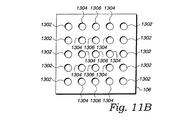
図11Bは、本発明の一実施形態における近接ヘッド106の一部を示した上面図である。図8Bを参照にして説明された近接ヘッド106の構成は、当然のことながら、代表的な性質のものである。したがって、流体メニスカスを生成するために用いられる近接ヘッドは、ウエハに対して処理液の供給および除去を行うことによってウエハ表面上に安定した流体メニスカスを生成することができる限り、他の構成を採ることが可能である。また、前述のように、N2/IPAを使用せずに流体メニスカスを生成する場合の近接ヘッド106の他の実施形態では、ソース供給口1316を必要としない。
FIG. 11B is a top view showing a part of the
一実施形態の上面図では、左から右に向かって、ソース供給口セット1302、ソース排出口セット1304、ソース供給口セット1306、ソース排出口セット1304、およびソース供給口セット1302の順である。したがって、N2/IPAおよび処理用化学剤が、近接ヘッド106とウエハ108との間の領域にインプットされるのに伴って、真空は、ウエハ108上に残留し得るあらゆる流体膜および汚染物の少なくとも一方と共に、N2/IPAおよび処理用の化学剤を除去する。本明細書で提示されるソース供給口1302、ソース供給口1306、およびソース排出口1304は、例えば円状の開口、三角形の開口、および四角形の開口などの任意の適切な種類の幾何学的形状とすることができる。一実施形態において、ソース供給口1302,1306およびソース排出口1304は、円状の開口を有する。当然のことながら、近接ヘッド106を、生成を所望される流体メニスカス106の大きさおよび形状に応じて、大きさ、形状、および構成の少なくとも一つが任意の適切なものとすることができる。一実施形態において、近接ヘッドは、ウエハの半径に満たない大きさであっても良い。別の一実施形態において、近接ヘッドは、ウエハの半径を超える大きさであっても良い。別の一実施形態において、近接ヘッドは、ウエハの直径を超える大きさであっても良い。したがって、流体メニスカスの大きさは、任意の所定時間内に処理されることが望ましいウエハ表面上の領域の大きさに応じ、任意の適切な大きさとすることができる。また、近接ヘッド106は、例えば水平、垂直、またはその中間の任意の適切な姿勢など、ウエハ処理工程に応じて任意の適切な向きに配置することができる。近接ヘッド106は、また、一つまたはそれ以上の種類のウエハ処理工程が実施されるウエハ処理システムに組み込まれても良い。
In the top view of one embodiment, from left to right, the source supply port set 1302, the source discharge port set 1304, the source supply port set 1306, the source discharge port set 1304, and the source supply port set 1302 are in this order. Thus, as N 2 / IPA and processing chemicals are input into the area between the
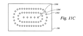
図11Cは、本発明の一実施形態における近接ヘッド106の供給口/排出口パターンを示している。この実施形態では、近接ヘッド106は、ソース供給口1302,1306およびソース排出口1304を含む。一実施形態において、ソース排出口1304はソース供給口1306を取り囲んでいても良く、ソース供給口1302はソース排出口1304を取り囲んでいても良い。
FIG. 11C shows the supply port / discharge port pattern of the
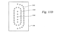
図11Dは、本発明の一実施形態における近接ヘッド106の別の供給口/排出口パターンを示している。この実施形態では、近接ヘッド106は、ソース供給口1302,1306およびソース排出口1304を含む。一実施形態において、ソース排出口1304はソース供給口1306を取り囲んでいても良く、ソース供給口1302はソース排出口1304を少なくとも部分的に取り囲んでいても良い。
FIG. 11D shows another supply / discharge port pattern of the
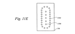
図11Eは、本発明の一実施形態における近接ヘッド106の更に別の供給口/排出口パターンを示している。この実施形態では、近接ヘッド106は、ソース供給口1302,1306およびソース排出口1304を含む。一実施形態において、ソース排出口1304は、ソース供給口1306を取り囲んでいても良い。一実施形態において、近接ヘッド106は、IPA/N2を供給することなく流体メニスカスを生成することができるので、この一実施形態において、近接ヘッド106は、ソース供給口1302を備えていない。なお、上述された供給口/排出口パターンは、代表的な性質のものであるので、安定した且つ制御可能な流体メニスカスを生成できる限り、任意の適切な種類の供給口/排出口パターンを用いることができる。
FIG. 11E shows yet another supply / discharge pattern of the
本発明は、いくつかの好ましい実施形態の観点から説明されたが、当業者ならば、これまでの明細書を熟読し且つ図面を検討することによって、各種の代替、追加、置換、および等価物の形態を想到できることは、言うまでもない。したがって、本発明は、本発明の真の趣旨および範囲の範囲内において、このようなあらゆる代替、追加、置換、および等価物の形態を含むものと解釈される。 Although the present invention has been described in terms of several preferred embodiments, those skilled in the art will recognize various alternatives, additions, substitutions, and equivalents by reading the previous specification and reviewing the drawings. It goes without saying that this form can be conceived. Accordingly, the present invention is to be construed as including all such alternatives, additions, substitutions and equivalents within the true spirit and scope of the present invention.
10…ウエハ
12…液体と気体との移動境界面
100…ウエハ処理システム
102…ローラ
104…アーム
106…近接ヘッド
108…ウエハ
108a…ウエハの上面
108b…ウエハの下面
120…ドッキングステーション
122…上部
124…下部
126…クーポンマガジン
128…クーポンマガジンマウント
140…流体メニスカス、覗き窓
202…取り付け穴
262…ボール止め
264…バネ
288…アクセスポート
290…ネジ
320…取り付け穴
322…窪み
380…窪み
390…取り付け穴
392…凹所
1100…ウエハ処理システム
1102…ローラ
1104…アーム
1302…ソース供給口
1304…ソース排出口
1306…ソース供給口
1310…IPA/N2
1312…真空
1314…処理液
DESCRIPTION OF
1312 ... Vacuum 1314 ... Treatment liquid
Claims (20)
前記基板の端部に隣接して前記基板とほぼ同一平面内に配置されるように構成されるドッキング表面であって、移動境界面を提供することによって前記流体メニスカスが前記基板の表面に出入りすることを可能にするドッキング表面を備える装置。 An apparatus for treating a substrate with a fluid meniscus supplied to the surface of the substrate,
A docking surface that is configured to be disposed in substantially the same plane as the substrate adjacent to an edge of the substrate, wherein the fluid meniscus enters and exits the surface of the substrate by providing a moving interface. A device with a docking surface that makes it possible.
前記ドッキング表面は、前記流体メニスカスのためのドッキングステーションを構成する、装置。 An apparatus for processing a substrate according to claim 1, comprising:
The apparatus wherein the docking surface constitutes a docking station for the fluid meniscus.
前記ドッキング表面を含む前記ドッキングステーションを保持するためのクーポンマガジンを備える装置。 An apparatus for processing a substrate according to claim 2, further comprising:
An apparatus comprising a coupon magazine for holding the docking station including the docking surface.
前記ドッキング表面は、前記基板の外周形状に合致する外周形状を有する、装置。 An apparatus for processing a substrate according to claim 1, comprising:
The apparatus wherein the docking surface has an outer peripheral shape that matches the outer peripheral shape of the substrate.
近接ヘッドのためのドッキングステーションを前記基板の端部に隣接する位置に保持するように構成されるクーポンマガジンを備える装置。 An apparatus for use in processing a substrate,
An apparatus comprising a coupon magazine configured to hold a docking station for a proximity head in a position adjacent to an edge of the substrate.
前記ドッキングステーションは、前記近接ヘッドの流体メニスカスのための移動境界面を提供するドッキング表面によって構成される、装置。 An apparatus for use in processing a substrate according to claim 5, comprising:
The apparatus, wherein the docking station is constituted by a docking surface that provides a moving interface for a fluid meniscus of the proximity head.
前記クーポンマガジンは、上部および下部を含む、装置。 An apparatus for use in processing a substrate according to claim 5, comprising:
The coupon magazine includes an upper portion and a lower portion.
前記ドッキングステーションは、前記上部と前記下部との間に保持される、装置。 An apparatus for use in processing a substrate according to claim 7,
The apparatus, wherein the docking station is held between the upper part and the lower part.
前記ドッキングステーションは、石英材料である、装置。 An apparatus for use in processing a substrate according to claim 5, comprising:
The apparatus wherein the docking station is a quartz material.
前記ドッキングステーションは、親水性材料である、装置。 An apparatus for use in processing a substrate according to claim 5, comprising:
The apparatus, wherein the docking station is a hydrophilic material.
前記クーポンマガジンを保持するように構成されるクーポンマガジンマウントを備える装置。 An apparatus for use in processing a substrate according to claim 5, further comprising:
An apparatus comprising a coupon magazine mount configured to hold the coupon magazine.
前記ドッキングステーションを前記基板とほぼ共平面上に移動させるように構成されるレベリング機構を備える装置。 An apparatus for use in processing a substrate according to claim 5, further comprising:
An apparatus comprising a leveling mechanism configured to move the docking station substantially coplanar with the substrate.
前記レベリング機構は、前記ドッキングステーションを垂直面内で移動させるように構成される、装置。 An apparatus for use in processing a substrate according to claim 12,
The apparatus, wherein the leveling mechanism is configured to move the docking station in a vertical plane.
前記レベリング機構は、ボール止めを垂直に移動させるように構成されるネジを含む、装置。 An apparatus for use in processing a substrate according to claim 12,
The apparatus wherein the leveling mechanism includes a screw configured to move the ball stop vertically.
前記クーポンマガジンは、覗き窓を含む、装置。 An apparatus for use in processing a substrate according to claim 5, comprising:
The coupon magazine includes a viewing window.
基板表面とほぼ共平面上に前記基板の端部に隣接して移動表面を配置する工程と、
前記移動表面と前記基板表面との間で流体メニスカスを移動させる工程と
を備える方法。 A method for processing a substrate, comprising:
Placing a moving surface adjacent to an edge of the substrate substantially coplanar with the substrate surface;
Moving a fluid meniscus between the moving surface and the substrate surface.
前記移動表面を配置する工程は、前記移動表面の高さを調整することを含む、方法。 A method for processing a substrate according to claim 16, comprising the steps of:
Placing the moving surface comprises adjusting a height of the moving surface.
前記高さ調整は、前記レベリング機構によって実現される、方法。 A method for processing a substrate according to claim 17, comprising:
The height adjustment is realized by the leveling mechanism.
前記移動表面は、親水性材料である、方法。 A method for processing a substrate according to claim 16, comprising the steps of:
The method wherein the moving surface is a hydrophilic material.
前記移動表面と前記基板表面との間で流体メニスカスを移動させる工程は、前記流体メニスカスを前記基板表面上から前記移動表面上へと移動させること、および、前記流体メニスカスを前記移動表面上から前記基板表面上へと移動させること、の一方を含む、方法。 A method for processing a substrate according to claim 16, comprising the steps of:
The step of moving a fluid meniscus between the moving surface and the substrate surface includes moving the fluid meniscus from on the substrate surface to the moving surface, and moving the fluid meniscus from above the moving surface. Moving the substrate onto a surface of the substrate.
Applications Claiming Priority (1)
| Application Number | Priority Date | Filing Date | Title |
|---|---|---|---|
| US10/817,620 US7513262B2 (en) | 2002-09-30 | 2004-04-01 | Substrate meniscus interface and methods for operation |
Publications (2)
| Publication Number | Publication Date |
|---|---|
| JP2005294835A true JP2005294835A (en) | 2005-10-20 |
| JP4621055B2 JP4621055B2 (en) | 2011-01-26 |
Family
ID=34887787
Family Applications (1)
| Application Number | Title | Priority Date | Filing Date |
|---|---|---|---|
| JP2005100372A Expired - Fee Related JP4621055B2 (en) | 2004-04-01 | 2005-03-31 | Interface between the substrate and the meniscus and the handling method thereof |
Country Status (8)
| Country | Link |
|---|---|
| US (1) | US7513262B2 (en) |
| EP (1) | EP1583137B1 (en) |
| JP (1) | JP4621055B2 (en) |
| KR (1) | KR101168183B1 (en) |
| CN (1) | CN1722373B (en) |
| AT (1) | ATE515058T1 (en) |
| MY (1) | MY141428A (en) |
| SG (2) | SG115839A1 (en) |
Cited By (1)
| Publication number | Priority date | Publication date | Assignee | Title |
|---|---|---|---|---|
| JP2009524258A (en) * | 2006-01-20 | 2009-06-25 | アクリオン テクノロジーズ インク | Acoustic energy system, method and apparatus for processing flat objects |
Families Citing this family (32)
| Publication number | Priority date | Publication date | Assignee | Title |
|---|---|---|---|---|
| US7234477B2 (en) * | 2000-06-30 | 2007-06-26 | Lam Research Corporation | Method and apparatus for drying semiconductor wafer surfaces using a plurality of inlets and outlets held in close proximity to the wafer surfaces |
| US20040031167A1 (en) | 2002-06-13 | 2004-02-19 | Stein Nathan D. | Single wafer method and apparatus for drying semiconductor substrates using an inert gas air-knife |
| US7367345B1 (en) | 2002-09-30 | 2008-05-06 | Lam Research Corporation | Apparatus and method for providing a confined liquid for immersion lithography |
| US7383843B2 (en) * | 2002-09-30 | 2008-06-10 | Lam Research Corporation | Method and apparatus for processing wafer surfaces using thin, high velocity fluid layer |
| US7513262B2 (en) | 2002-09-30 | 2009-04-07 | Lam Research Corporation | Substrate meniscus interface and methods for operation |
| US7198055B2 (en) * | 2002-09-30 | 2007-04-03 | Lam Research Corporation | Meniscus, vacuum, IPA vapor, drying manifold |
| US7997288B2 (en) * | 2002-09-30 | 2011-08-16 | Lam Research Corporation | Single phase proximity head having a controlled meniscus for treating a substrate |
| US7153400B2 (en) * | 2002-09-30 | 2006-12-26 | Lam Research Corporation | Apparatus and method for depositing and planarizing thin films of semiconductor wafers |
| US7293571B2 (en) | 2002-09-30 | 2007-11-13 | Lam Research Corporation | Substrate proximity processing housing and insert for generating a fluid meniscus |
| US8236382B2 (en) * | 2002-09-30 | 2012-08-07 | Lam Research Corporation | Proximity substrate preparation sequence, and method, apparatus, and system for implementing the same |
| US7632376B1 (en) | 2002-09-30 | 2009-12-15 | Lam Research Corporation | Method and apparatus for atomic layer deposition (ALD) in a proximity system |
| US7389783B2 (en) * | 2002-09-30 | 2008-06-24 | Lam Research Corporation | Proximity meniscus manifold |
| US7614411B2 (en) | 2002-09-30 | 2009-11-10 | Lam Research Corporation | Controls of ambient environment during wafer drying using proximity head |
| US7675000B2 (en) * | 2003-06-24 | 2010-03-09 | Lam Research Corporation | System method and apparatus for dry-in, dry-out, low defect laser dicing using proximity technology |
| US8062471B2 (en) * | 2004-03-31 | 2011-11-22 | Lam Research Corporation | Proximity head heating method and apparatus |
| US7928366B2 (en) * | 2006-10-06 | 2011-04-19 | Lam Research Corporation | Methods of and apparatus for accessing a process chamber using a dual zone gas injector with improved optical access |
| US8813764B2 (en) | 2009-05-29 | 2014-08-26 | Lam Research Corporation | Method and apparatus for physical confinement of a liquid meniscus over a semiconductor wafer |
| US7946303B2 (en) | 2006-09-29 | 2011-05-24 | Lam Research Corporation | Carrier for reducing entrance and/or exit marks left by a substrate-processing meniscus |
| JP4755573B2 (en) * | 2006-11-30 | 2011-08-24 | 東京応化工業株式会社 | Processing apparatus and processing method, and surface treatment jig |
| US8146902B2 (en) * | 2006-12-21 | 2012-04-03 | Lam Research Corporation | Hybrid composite wafer carrier for wet clean equipment |
| US8464736B1 (en) | 2007-03-30 | 2013-06-18 | Lam Research Corporation | Reclaim chemistry |
| US7975708B2 (en) * | 2007-03-30 | 2011-07-12 | Lam Research Corporation | Proximity head with angled vacuum conduit system, apparatus and method |
| US8141566B2 (en) * | 2007-06-19 | 2012-03-27 | Lam Research Corporation | System, method and apparatus for maintaining separation of liquids in a controlled meniscus |
| JP4971078B2 (en) * | 2007-08-30 | 2012-07-11 | 東京応化工業株式会社 | Surface treatment equipment |
| US9111729B2 (en) * | 2009-12-03 | 2015-08-18 | Lam Research Corporation | Small plasma chamber systems and methods |
| US9190289B2 (en) | 2010-02-26 | 2015-11-17 | Lam Research Corporation | System, method and apparatus for plasma etch having independent control of ion generation and dissociation of process gas |
| US9967965B2 (en) | 2010-08-06 | 2018-05-08 | Lam Research Corporation | Distributed, concentric multi-zone plasma source systems, methods and apparatus |
| US9155181B2 (en) | 2010-08-06 | 2015-10-06 | Lam Research Corporation | Distributed multi-zone plasma source systems, methods and apparatus |
| US8999104B2 (en) | 2010-08-06 | 2015-04-07 | Lam Research Corporation | Systems, methods and apparatus for separate plasma source control |
| US9449793B2 (en) | 2010-08-06 | 2016-09-20 | Lam Research Corporation | Systems, methods and apparatus for choked flow element extraction |
| US9177762B2 (en) | 2011-11-16 | 2015-11-03 | Lam Research Corporation | System, method and apparatus of a wedge-shaped parallel plate plasma reactor for substrate processing |
| US10283325B2 (en) | 2012-10-10 | 2019-05-07 | Lam Research Corporation | Distributed multi-zone plasma source systems, methods and apparatus |
Citations (4)
| Publication number | Priority date | Publication date | Assignee | Title |
|---|---|---|---|---|
| JPH06273919A (en) * | 1993-03-19 | 1994-09-30 | Sharp Corp | Cleaning device |
| JPH11233475A (en) * | 1998-02-12 | 1999-08-27 | Sony Corp | Substrate cleaning device |
| JP2000271524A (en) * | 1999-03-25 | 2000-10-03 | Tokyo Electron Ltd | Processing device and processing method |
| JP2003332286A (en) * | 2002-04-15 | 2003-11-21 | Samsung Electronics Co Ltd | Semiconductor wafer cleaning apparatus and cleaning method using the same |
Family Cites Families (97)
| Publication number | Priority date | Publication date | Assignee | Title |
|---|---|---|---|---|
| US3953265A (en) | 1975-04-28 | 1976-04-27 | International Business Machines Corporation | Meniscus-contained method of handling fluids in the manufacture of semiconductor wafers |
| US4086870A (en) * | 1977-06-30 | 1978-05-02 | International Business Machines Corporation | Novel resist spinning head |
| US4367123A (en) | 1980-07-09 | 1983-01-04 | Olin Corporation | Precision spot plating process and apparatus |
| JPS5852034B2 (en) | 1981-08-26 | 1983-11-19 | 株式会社ソニツクス | Partial plating method and device |
| US4444492A (en) | 1982-05-15 | 1984-04-24 | General Signal Corporation | Apparatus for projecting a series of images onto dies of a semiconductor wafer |
| US4838289A (en) * | 1982-08-03 | 1989-06-13 | Texas Instruments Incorporated | Apparatus and method for edge cleaning |
| JPS62150828A (en) | 1985-12-25 | 1987-07-04 | Mitsubishi Electric Corp | Wafer drying apparatus |
| JPH0712035B2 (en) | 1989-04-20 | 1995-02-08 | 三菱電機株式会社 | Jet type liquid treatment device |
| JPH02309638A (en) | 1989-05-24 | 1990-12-25 | Fujitsu Ltd | Wafer etching device |
| JPH0628223Y2 (en) | 1989-06-14 | 1994-08-03 | 大日本スクリーン製造株式会社 | Spin coating device |
| US5271774A (en) * | 1990-03-01 | 1993-12-21 | U.S. Philips Corporation | Method for removing in a centrifuge a liquid from a surface of a substrate |
| US5102494A (en) | 1990-07-13 | 1992-04-07 | Mobil Solar Energy Corporation | Wet-tip die for EFG cyrstal growth apparatus |
| US5294257A (en) * | 1991-10-28 | 1994-03-15 | International Business Machines Corporation | Edge masking spin tool |
| US5343234A (en) | 1991-11-15 | 1994-08-30 | Kuehnle Manfred R | Digital color proofing system and method for offset and gravure printing |
| US5749469A (en) * | 1992-05-15 | 1998-05-12 | Fluoroware, Inc. | Wafer carrier |
| JP2877216B2 (en) | 1992-10-02 | 1999-03-31 | 東京エレクトロン株式会社 | Cleaning equipment |
| US5350502A (en) * | 1992-12-29 | 1994-09-27 | E. I. Du Pont De Nemours And Company | Apparatus for fluid treatment of framed membranes |
| US5472502A (en) | 1993-08-30 | 1995-12-05 | Semiconductor Systems, Inc. | Apparatus and method for spin coating wafers and the like |
| US5807522A (en) * | 1994-06-17 | 1998-09-15 | The Board Of Trustees Of The Leland Stanford Junior University | Methods for fabricating microarrays of biological samples |
| HU222768B1 (en) * | 1994-06-30 | 2003-10-28 | The Procter & Gamble Company | Liquid transport web with surface energy gradient, method for producing and absorbent article containing it |
| US5705223A (en) * | 1994-07-26 | 1998-01-06 | International Business Machine Corp. | Method and apparatus for coating a semiconductor wafer |
| JP3247270B2 (en) | 1994-08-25 | 2002-01-15 | 東京エレクトロン株式会社 | Processing apparatus and dry cleaning method |
| US5558111A (en) | 1995-02-02 | 1996-09-24 | International Business Machines Corporation | Apparatus and method for carrier backing film reconditioning |
| US5601655A (en) | 1995-02-14 | 1997-02-11 | Bok; Hendrik F. | Method of cleaning substrates |
| JPH08277486A (en) | 1995-04-04 | 1996-10-22 | Dainippon Printing Co Ltd | Lead frame plating equipment |
| TW386235B (en) * | 1995-05-23 | 2000-04-01 | Tokyo Electron Ltd | Method for spin rinsing |
| US5660642A (en) * | 1995-05-26 | 1997-08-26 | The Regents Of The University Of California | Moving zone Marangoni drying of wet objects using naturally evaporated solvent vapor |
| US5975098A (en) * | 1995-12-21 | 1999-11-02 | Dainippon Screen Mfg. Co., Ltd. | Apparatus for and method of cleaning substrate |
| DE19622015A1 (en) * | 1996-05-31 | 1997-12-04 | Siemens Ag | Process for etching destruction zones on a semiconductor substrate edge and etching system |
| US5985031A (en) | 1996-06-21 | 1999-11-16 | Micron Technology, Inc. | Spin coating spindle and chuck assembly |
| TW357406B (en) * | 1996-10-07 | 1999-05-01 | Tokyo Electron Ltd | Method and apparatus for cleaning and drying a substrate |
| DE19646006C2 (en) * | 1996-11-07 | 2000-04-06 | Hideyuki Kobayashi | Quick plating nozzle with a plating solution blasting and suction function |
| JPH1133506A (en) | 1997-07-24 | 1999-02-09 | Tadahiro Omi | Fluid treatment device and cleaning treatment system |
| JPH10163138A (en) | 1996-11-29 | 1998-06-19 | Fujitsu Ltd | Semiconductor device manufacturing method and polishing apparatus |
| JPH10232498A (en) | 1997-02-19 | 1998-09-02 | Nec Kyushu Ltd | Developing device |
| US6247479B1 (en) * | 1997-05-27 | 2001-06-19 | Tokyo Electron Limited | Washing/drying process apparatus and washing/drying process method |
| JPH1131672A (en) | 1997-07-10 | 1999-02-02 | Hitachi Ltd | Substrate processing method and substrate processing apparatus |
| US6103636A (en) | 1997-08-20 | 2000-08-15 | Micron Technology, Inc. | Method and apparatus for selective removal of material from wafer alignment marks |
| EP0970511B1 (en) | 1997-09-24 | 2005-01-12 | Interuniversitair Micro-Elektronica Centrum Vzw | Method and apparatus for removing a liquid from a surface |
| US6491764B2 (en) * | 1997-09-24 | 2002-12-10 | Interuniversitair Microelektronics Centrum (Imec) | Method and apparatus for removing a liquid from a surface of a rotating substrate |
| DE69832567T2 (en) | 1997-09-24 | 2007-01-18 | Interuniversitair Micro-Electronica Centrum Vzw | Method and apparatus for removing liquid from the surface of a rotating substrate |
| US6398975B1 (en) * | 1997-09-24 | 2002-06-04 | Interuniversitair Microelektronica Centrum (Imec) | Method and apparatus for localized liquid treatment of the surface of a substrate |
| EP0905746A1 (en) | 1997-09-24 | 1999-03-31 | Interuniversitair Micro-Elektronica Centrum Vzw | Method of removing a liquid from a surface of a rotating substrate |
| JP3523197B2 (en) * | 1998-02-12 | 2004-04-26 | エーシーエム リサーチ,インコーポレイティド | Plating equipment and method |
| WO1999049504A1 (en) | 1998-03-26 | 1999-09-30 | Nikon Corporation | Projection exposure method and system |
| US6108932A (en) | 1998-05-05 | 2000-08-29 | Steag Microtech Gmbh | Method and apparatus for thermocapillary drying |
| JPH11350169A (en) | 1998-06-10 | 1999-12-21 | Chemitoronics Co | Wet etching apparatus and wet etching method |
| US6132586A (en) * | 1998-06-11 | 2000-10-17 | Integrated Process Equipment Corporation | Method and apparatus for non-contact metal plating of semiconductor wafers using a bipolar electrode assembly |
| US6689323B2 (en) | 1998-10-30 | 2004-02-10 | Agilent Technologies | Method and apparatus for liquid transfer |
| US6715944B2 (en) * | 1998-11-12 | 2004-04-06 | Mitsubishi Denki Kabushiki Kaisha | Apparatus for removing photoresist film |
| US6092937A (en) | 1999-01-08 | 2000-07-25 | Fastar, Ltd. | Linear developer |
| JP3653198B2 (en) * | 1999-07-16 | 2005-05-25 | アルプス電気株式会社 | Nozzle for drying, drying apparatus and cleaning apparatus using the same |
| US20020121290A1 (en) * | 1999-08-25 | 2002-09-05 | Applied Materials, Inc. | Method and apparatus for cleaning/drying hydrophobic wafers |
| JP3635217B2 (en) * | 1999-10-05 | 2005-04-06 | 東京エレクトロン株式会社 | Liquid processing apparatus and method |
| WO2001027357A1 (en) | 1999-10-12 | 2001-04-19 | Semitool, Inc. | Method and apparatus for executing plural processes on a microelectronic workpiece at a single processing station |
| US6341998B1 (en) * | 1999-11-04 | 2002-01-29 | Vlsi Technology, Inc. | Integrated circuit (IC) plating deposition system and method |
| US6162302A (en) * | 1999-11-16 | 2000-12-19 | Agilent Technologies | Method of cleaning quartz substrates using conductive solutions |
| US6214513B1 (en) | 1999-11-24 | 2001-04-10 | Xerox Corporation | Slot coating under an electric field |
| US6433541B1 (en) | 1999-12-23 | 2002-08-13 | Kla-Tencor Corporation | In-situ metalization monitoring using eddy current measurements during the process for removing the film |
| US20030091754A1 (en) | 2000-02-11 | 2003-05-15 | Thami Chihani | Method for treating cellulosic fibres |
| US6474786B2 (en) | 2000-02-24 | 2002-11-05 | The Board Of Trustees Of The Leland Stanford Junior University | Micromachined two-dimensional array droplet ejectors |
| US6495005B1 (en) | 2000-05-01 | 2002-12-17 | International Business Machines Corporation | Electroplating apparatus |
| AU2001261625B2 (en) | 2000-05-16 | 2006-04-06 | Regents Of The University Of Minnesota | High mass throughput particle generation using multiple nozzle spraying |
| AU2001270205A1 (en) | 2000-06-26 | 2002-01-08 | Applied Materials, Inc. | Method and apparatus for wafer cleaning |
| US7234477B2 (en) | 2000-06-30 | 2007-06-26 | Lam Research Corporation | Method and apparatus for drying semiconductor wafer surfaces using a plurality of inlets and outlets held in close proximity to the wafer surfaces |
| US7000622B2 (en) | 2002-09-30 | 2006-02-21 | Lam Research Corporation | Methods and systems for processing a bevel edge of a substrate using a dynamic liquid meniscus |
| US6488040B1 (en) * | 2000-06-30 | 2002-12-03 | Lam Research Corporation | Capillary proximity heads for single wafer cleaning and drying |
| US6530823B1 (en) | 2000-08-10 | 2003-03-11 | Nanoclean Technologies Inc | Methods for cleaning surfaces substantially free of contaminants |
| JP2002075947A (en) * | 2000-08-30 | 2002-03-15 | Alps Electric Co Ltd | Wet processing equipment |
| US6555017B1 (en) | 2000-10-13 | 2003-04-29 | The Regents Of The University Of Caliofornia | Surface contouring by controlled application of processing fluid using Marangoni effect |
| US6550988B2 (en) | 2000-10-30 | 2003-04-22 | Dainippon Screen Mfg., Co., Ltd. | Substrate processing apparatus |
| US6531206B2 (en) * | 2001-02-07 | 2003-03-11 | 3M Innovative Properties Company | Microstructured surface film assembly for liquid acquisition and transport |
| WO2002101798A2 (en) | 2001-06-12 | 2002-12-19 | Verteq, Inc. | Method of applying liquid to a megasonic apparatus for improved cleaning control |
| TW554069B (en) | 2001-08-10 | 2003-09-21 | Ebara Corp | Plating device and method |
| JP2003115474A (en) | 2001-10-03 | 2003-04-18 | Ebara Corp | Substrate processing apparatus and method |
| JP4003441B2 (en) | 2001-11-08 | 2007-11-07 | セイコーエプソン株式会社 | Surface treatment apparatus and surface treatment method |
| US6799584B2 (en) | 2001-11-09 | 2004-10-05 | Applied Materials, Inc. | Condensation-based enhancement of particle removal by suction |
| US7513262B2 (en) | 2002-09-30 | 2009-04-07 | Lam Research Corporation | Substrate meniscus interface and methods for operation |
| US7614411B2 (en) | 2002-09-30 | 2009-11-10 | Lam Research Corporation | Controls of ambient environment during wafer drying using proximity head |
| US7093375B2 (en) | 2002-09-30 | 2006-08-22 | Lam Research Corporation | Apparatus and method for utilizing a meniscus in substrate processing |
| PL208010B1 (en) | 2002-09-30 | 2011-03-31 | Lam Res Corp | System for substrate processing with meniscus, vacuum, ipa vapor, drying manifold |
| US7153400B2 (en) | 2002-09-30 | 2006-12-26 | Lam Research Corporation | Apparatus and method for depositing and planarizing thin films of semiconductor wafers |
| US7383843B2 (en) | 2002-09-30 | 2008-06-10 | Lam Research Corporation | Method and apparatus for processing wafer surfaces using thin, high velocity fluid layer |
| US6988326B2 (en) | 2002-09-30 | 2006-01-24 | Lam Research Corporation | Phobic barrier meniscus separation and containment |
| US7252097B2 (en) | 2002-09-30 | 2007-08-07 | Lam Research Corporation | System and method for integrating in-situ metrology within a wafer process |
| US6988327B2 (en) | 2002-09-30 | 2006-01-24 | Lam Research Corporation | Methods and systems for processing a substrate using a dynamic liquid meniscus |
| US7389783B2 (en) | 2002-09-30 | 2008-06-24 | Lam Research Corporation | Proximity meniscus manifold |
| US6954993B1 (en) | 2002-09-30 | 2005-10-18 | Lam Research Corporation | Concentric proximity processing head |
| US7293571B2 (en) | 2002-09-30 | 2007-11-13 | Lam Research Corporation | Substrate proximity processing housing and insert for generating a fluid meniscus |
| US7198055B2 (en) | 2002-09-30 | 2007-04-03 | Lam Research Corporation | Meniscus, vacuum, IPA vapor, drying manifold |
| US7069937B2 (en) | 2002-09-30 | 2006-07-04 | Lam Research Corporation | Vertical proximity processor |
| SG121822A1 (en) | 2002-11-12 | 2006-05-26 | Asml Netherlands Bv | Lithographic apparatus and device manufacturing method |
| US7270137B2 (en) * | 2003-04-28 | 2007-09-18 | Tokyo Electron Limited | Apparatus and method of securing a workpiece during high-pressure processing |
| EP1489461A1 (en) | 2003-06-11 | 2004-12-22 | ASML Netherlands B.V. | Lithographic apparatus and device manufacturing method |
| US6867844B2 (en) | 2003-06-19 | 2005-03-15 | Asml Holding N.V. | Immersion photolithography system and method using microchannel nozzles |
| US7353560B2 (en) | 2003-12-18 | 2008-04-08 | Lam Research Corporation | Proximity brush unit apparatus and method |
| US7003899B1 (en) | 2004-09-30 | 2006-02-28 | Lam Research Corporation | System and method for modulating flow through multiple ports in a proximity head |
-
2004
- 2004-04-01 US US10/817,620 patent/US7513262B2/en not_active Expired - Fee Related
-
2005
- 2005-03-23 SG SG200502528A patent/SG115839A1/en unknown
- 2005-03-23 SG SG200708776-0A patent/SG136141A1/en unknown
- 2005-03-29 AT AT05251903T patent/ATE515058T1/en not_active IP Right Cessation
- 2005-03-29 EP EP05251903A patent/EP1583137B1/en not_active Expired - Lifetime
- 2005-03-31 JP JP2005100372A patent/JP4621055B2/en not_active Expired - Fee Related
- 2005-04-01 MY MYPI20051479A patent/MY141428A/en unknown
- 2005-04-01 CN CN2005100741974A patent/CN1722373B/en not_active Expired - Fee Related
- 2005-04-01 KR KR1020050027441A patent/KR101168183B1/en not_active Expired - Fee Related
Patent Citations (4)
| Publication number | Priority date | Publication date | Assignee | Title |
|---|---|---|---|---|
| JPH06273919A (en) * | 1993-03-19 | 1994-09-30 | Sharp Corp | Cleaning device |
| JPH11233475A (en) * | 1998-02-12 | 1999-08-27 | Sony Corp | Substrate cleaning device |
| JP2000271524A (en) * | 1999-03-25 | 2000-10-03 | Tokyo Electron Ltd | Processing device and processing method |
| JP2003332286A (en) * | 2002-04-15 | 2003-11-21 | Samsung Electronics Co Ltd | Semiconductor wafer cleaning apparatus and cleaning method using the same |
Cited By (1)
| Publication number | Priority date | Publication date | Assignee | Title |
|---|---|---|---|---|
| JP2009524258A (en) * | 2006-01-20 | 2009-06-25 | アクリオン テクノロジーズ インク | Acoustic energy system, method and apparatus for processing flat objects |
Also Published As
| Publication number | Publication date |
|---|---|
| JP4621055B2 (en) | 2011-01-26 |
| MY141428A (en) | 2010-04-30 |
| US7513262B2 (en) | 2009-04-07 |
| SG136141A1 (en) | 2007-10-29 |
| EP1583137B1 (en) | 2011-06-29 |
| US20050145268A1 (en) | 2005-07-07 |
| CN1722373B (en) | 2011-09-28 |
| EP1583137A3 (en) | 2006-04-19 |
| ATE515058T1 (en) | 2011-07-15 |
| CN1722373A (en) | 2006-01-18 |
| KR20060045411A (en) | 2006-05-17 |
| EP1583137A2 (en) | 2005-10-05 |
| KR101168183B1 (en) | 2012-07-24 |
| SG115839A1 (en) | 2005-10-28 |
Similar Documents
| Publication | Publication Date | Title |
|---|---|---|
| JP4621055B2 (en) | Interface between the substrate and the meniscus and the handling method thereof | |
| US7731802B2 (en) | Methods for transitioning a fluid meniscus to and from surfaces of a substrate | |
| JP4589866B2 (en) | Substrate processing system using meniscus, vacuum, IPA vapor, drying manifold | |
| EP1582269B1 (en) | Proximity meniscus manifold | |
| JP4758694B2 (en) | Proximity proximity process head | |
| JP4759300B2 (en) | Method and apparatus for processing a wafer surface using a thin high velocity fluid layer | |
| JP4630103B2 (en) | Control of ambient environment during wafer drying using proximity head | |
| US7069937B2 (en) | Vertical proximity processor | |
| JP2006501655A (en) | Method and apparatus for drying a semiconductor wafer surface using a plurality of inlets and outlets held in close proximity to the wafer surface |
Legal Events
| Date | Code | Title | Description |
|---|---|---|---|
| A621 | Written request for application examination |
Free format text: JAPANESE INTERMEDIATE CODE: A621 Effective date: 20080319 |
|
| A131 | Notification of reasons for refusal |
Free format text: JAPANESE INTERMEDIATE CODE: A131 Effective date: 20100323 |
|
| A601 | Written request for extension of time |
Free format text: JAPANESE INTERMEDIATE CODE: A601 Effective date: 20100622 |
|
| A602 | Written permission of extension of time |
Free format text: JAPANESE INTERMEDIATE CODE: A602 Effective date: 20100625 |
|
| A521 | Request for written amendment filed |
Free format text: JAPANESE INTERMEDIATE CODE: A523 Effective date: 20100922 |
|
| TRDD | Decision of grant or rejection written | ||
| A01 | Written decision to grant a patent or to grant a registration (utility model) |
Free format text: JAPANESE INTERMEDIATE CODE: A01 Effective date: 20101012 |
|
| A01 | Written decision to grant a patent or to grant a registration (utility model) |
Free format text: JAPANESE INTERMEDIATE CODE: A01 |
|
| A61 | First payment of annual fees (during grant procedure) |
Free format text: JAPANESE INTERMEDIATE CODE: A61 Effective date: 20101029 |
|
| FPAY | Renewal fee payment (event date is renewal date of database) |
Free format text: PAYMENT UNTIL: 20131105 Year of fee payment: 3 |
|
| R150 | Certificate of patent or registration of utility model |
Free format text: JAPANESE INTERMEDIATE CODE: R150 |
|
| LAPS | Cancellation because of no payment of annual fees |