JP2005294812A - Boron phosphide based semiconductor device - Google Patents
Boron phosphide based semiconductor device Download PDFInfo
- Publication number
- JP2005294812A JP2005294812A JP2005061866A JP2005061866A JP2005294812A JP 2005294812 A JP2005294812 A JP 2005294812A JP 2005061866 A JP2005061866 A JP 2005061866A JP 2005061866 A JP2005061866 A JP 2005061866A JP 2005294812 A JP2005294812 A JP 2005294812A
- Authority
- JP
- Japan
- Prior art keywords
- type
- layer
- boron phosphide
- based semiconductor
- ohmic electrode
- Prior art date
- Legal status (The legal status is an assumption and is not a legal conclusion. Google has not performed a legal analysis and makes no representation as to the accuracy of the status listed.)
- Granted
Links
Images
Landscapes
- Electrodes Of Semiconductors (AREA)
- Led Devices (AREA)
Abstract
Description
本発明は、少なくともp形リン化硼素系半導体層とその上に形成したp形オーミック電極と備えるリン化硼素系半導体素子に関するものである。 The present invention relates to a boron phosphide-based semiconductor element including at least a p-type boron phosphide-based semiconductor layer and a p-type ohmic electrode formed thereon.
従来から、n形またはp形のリン化硼素(BP)系半導体層を利用して、発光ダイオード(LED)やレーザダイオード(LD)等のリン化硼素系半導体発光素子が作製されている(例えば特許文献1参照)。リン化硼素系半導体とは、此処では、硼素(元素記号:B)とリン(元素記号:P)との双方を必須の構成元素として含むIII−V族化合物半導体である。
リン化硼素系半導体発光素子は、例えばn形またはp形のリン化硼素系半導体層からなるコンタクト層に、オーミック電極を設けて作製される。p形のリン化硼素系半導体層に設けるp形オーミック電極は、従来から、金(Au)・亜鉛(Zn)合金から構成されている(例えば特許文献2参照)。アルミニウム(Al)単体からp形オーミック電極を形成する例も知られている(例えば非特許文献1参照)。また、リン化硼素系半導体に単量体のリン化硼素を用い、そのリン化硼素半導体層上に、ニッケル(Ni)からオーミック電極を形成できるのは公知である(例えば特許文献3参照)。
しかし、従来の電極材料では、p形リン化硼素系半導体層上に、接触抵抗の充分に低いp形オーミック電極を安定して形成できない。このため、例えばLEDでは、順方向電圧(Vf)の低下させるに妨げとなっているし、LDでは、閾値電圧(Vth)を低減させるのを困難としている。 However, the conventional electrode material cannot stably form a p-type ohmic electrode having a sufficiently low contact resistance on the p-type boron phosphide-based semiconductor layer. For this reason, for example, an LED hinders the forward voltage (Vf) from being lowered, and an LD makes it difficult to reduce the threshold voltage (Vth).
本発明は、上記に鑑みてなされたもので、p形リン化硼素系半導体層上に接触抵抗の充分に低いp形オーミック電極を安定して形成することができるリン化硼素系半導体素子を提供することを目的とする。 The present invention has been made in view of the above, and provides a boron phosphide-based semiconductor element capable of stably forming a p-type ohmic electrode having a sufficiently low contact resistance on a p-type boron phosphide-based semiconductor layer. The purpose is to do.
1)上記目的を達成するために、第1の発明は、少なくともp形リン化硼素系半導体層とその上に形成したp形オーミック電極とを備えるリン化硼素系半導体素子において、上記p形オーミック電極を、ニッケルと硼素との合金から構成した、ことを特徴としている。 1) To achieve the above object, according to a first aspect of the present invention, there is provided a boron phosphide-based semiconductor element including at least a p-type boron phosphide-based semiconductor layer and a p-type ohmic electrode formed thereon, The electrode is made of an alloy of nickel and boron.
2)第2の発明は、上記した1)項に記載の発明の構成に加えて、上記p形オーミック電極は、硼素の重量含有率が0%を超え25%未満である、ことを特徴としている。 2) The second invention is characterized in that, in addition to the structure of the invention described in the above item 1), the p-type ohmic electrode has a weight content of boron of more than 0% and less than 25%. Yes.
3)第3の発明は、上記した1)項または2)項に記載の発明の構成に加えて、上記p形リン化硼素系半導体層は、伝導形を制御するための不純物を故意に添加しないアンドープのリン化硼素から構成されている、ことを特徴としている。 3) In the third invention, in addition to the structure of the invention described in the above item 1) or 2), the p-type boron phosphide-based semiconductor layer is intentionally added with an impurity for controlling the conductivity type. It is characterized by being composed of undoped boron phosphide.
本発明では、p形リン化硼素系半導体層の表面に接触させて設けるp形オーミック電極をニッケルと硼素との合金膜から構成することとしたので、低接触抵抗のオーミック電極を形成することができ、したがって、順方向電圧を低くし、且つ素子駆動電流を効率的に発光層に平面的に拡散させることができ、発光強度を高くすることができる。 In the present invention, since the p-type ohmic electrode provided in contact with the surface of the p-type boron phosphide-based semiconductor layer is composed of an alloy film of nickel and boron, an ohmic electrode having a low contact resistance can be formed. Therefore, the forward voltage can be lowered, the element driving current can be efficiently diffused in a plane in the light emitting layer, and the light emission intensity can be increased.
以下にこの発明の実施の形態を詳細に説明する。 Embodiments of the present invention will be described in detail below.
本発明に係るp形リン化硼素系半導体とは、硼素(B)とリン(P)とを必須の構成元素とするIII族化合物半導体である。例えば、BαAlβGaγIn1-α-β-γP1-δAsδ(0<α≦1、0≦β<1、0≦γ<1、0<α+β+γ≦1、0≦δ<1である。また、BαAlβGaγIn1-α-β-γP1-δNδ(0<α≦1、0≦β<1、0≦γ<1、0<α+β+γ≦1、0≦δ<1)である。またp形の単量体リン化硼素(BP)、p形リン化硼素・ガリウム・インジウム(組成式BαGaγIn1-α-γP:0<α≦1、0≦γ<1)である。また、p形窒化リン化硼素(組成式BP1-δNδ:0≦δ<1)やp形砒化リン化硼素(組成式BαP1-δAsδ)等の複数のV族元素を含む混晶である。 The p-type boron phosphide-based semiconductor according to the present invention is a group III compound semiconductor containing boron (B) and phosphorus (P) as essential constituent elements. For example, B α Al β Ga γ In 1-α-β-γ P 1-δ As δ (0 <α ≦ 1, 0 ≦ β <1, 0 ≦ γ <1, 0 <α + β + γ ≦ 1, 0 ≦ δ <1. Further, B α Al β Ga γ in 1-α-β-γ P 1-δ N δ (0 <α ≦ 1,0 ≦ β <1,0 ≦ γ <1,0 <α + β + γ ≦ 1, 0 ≦ δ <1) p-type monomer boron phosphide (BP), p-type boron phosphide / gallium / indium (composition formula B α Ga γ In 1-α-γ P: 0 <Α ≦ 1, 0 ≦ γ <1) Also, p - type boron nitride phosphide (composition formula BP 1-δ N δ : 0 ≦ δ <1) and p-type boron arsenide phosphide (composition formula B α P 1-δ As δ ) and the like.
p形リン化硼素系半導体層は、ハロゲン法、ハイドライド法やMOCVD(有機金属化学的気相堆積)法により形成できる。また、分子線エピタキシャル法でも形成できる。 The p-type boron phosphide-based semiconductor layer can be formed by a halogen method, a hydride method, or a MOCVD (metal organic chemical vapor deposition) method. It can also be formed by molecular beam epitaxy.
p形の単量体のリン化硼素層(BP層)は、トリエチル硼素(分子式:(C2H5)3B)とホスフィン(分子式:PH3)を原料とするMOCVD法で形成することができ、形成温度としては、1000℃〜1200℃の温度が適する。形成時の原料供給比率(=PH3/(C2H5)3B)は、10〜50とするのが適する。不純物を故意に添加しないアンドープのp形BP層は不純物の拡散に因る他層の変性を回避するのに効果がある。形成温度、V/III比率に加えて、形成速度を精密に制御すれば、禁止帯幅を2.8eV以上とする広禁止帯幅のp形リン化硼素層を形成することができる。 The p-type monomeric boron phosphide layer (BP layer) may be formed by MOCVD using triethylboron (molecular formula: (C 2 H 5 ) 3 B) and phosphine (molecular formula: PH 3 ) as raw materials. A temperature of 1000 ° C. to 1200 ° C. is suitable as the formation temperature. The raw material supply ratio (= PH 3 / (C 2 H 5 ) 3 B) at the time of formation is suitably 10-50. An undoped p-type BP layer to which impurities are not intentionally added is effective in avoiding modification of other layers due to impurity diffusion. If the formation speed is precisely controlled in addition to the formation temperature and the V / III ratio, a p-type boron phosphide layer having a wide forbidden band width of 2.8 eV or more can be formed.
本発明に係るリン化硼素系半導体素子は、結晶基板上に形成されたp形リン化硼素系半導体層を利用して構成する。p形リン化硼素系半導体層を設ける結晶基板は、リン化硼素系半導体素子によって、n形またはp形伝導性、または高抵抗或いは絶縁性の結晶材料から選択する。例えば、電気絶縁性のサファイア(α−Al2O3単結晶)や炭化珪素(SiC)、また高抵抗の珪素(Si)単結晶は、pn接合型トランジスタ用途の基板として好適に利用することができる。多結晶シリコンは、pn接合型太陽電池用途の基板材料として利用することができる。pn接合型LEDやLD等のリン化硼素系半導体発光素子或いは受光素子には、導電性の立方晶3C型、或いは六方晶4Hまたは6H型炭化珪素(SiC)単結晶、リン化ガリウム(GaP)単結晶などを基板として利用することができる。基板を単結晶材料とすると、結晶性のp形リン化硼素系半導体層を得るのに優位となるが、ホウケイ酸ガラス等の非晶質材料も基板として利用できる。 The boron phosphide-based semiconductor element according to the present invention is configured using a p-type boron phosphide-based semiconductor layer formed on a crystal substrate. The crystal substrate on which the p-type boron phosphide-based semiconductor layer is provided is selected from an n-type or p-type conductive, high-resistance or insulating crystal material, depending on the boron phosphide-based semiconductor element. For example, electrically insulating sapphire (α-Al 2 O 3 single crystal), silicon carbide (SiC), or high-resistance silicon (Si) single crystal can be suitably used as a substrate for pn junction type transistors. it can. Polycrystalline silicon can be used as a substrate material for pn junction solar cell applications. For boron phosphide-based semiconductor light emitting devices or light receiving devices such as pn junction type LEDs and LDs, conductive cubic 3C type, hexagonal 4H or 6H type silicon carbide (SiC) single crystal, gallium phosphide (GaP) A single crystal or the like can be used as the substrate. When the substrate is a single crystal material, it is advantageous for obtaining a crystalline p-type boron phosphide-based semiconductor layer, but an amorphous material such as borosilicate glass can also be used as the substrate.
上記基板の表面に、直接接合させたのとは別に、基板上に形成したIII−V族化合物半導体層上に設けたp形リン化硼素系半導体層も、リン化硼素系半導体発光素子を構成するのに利用できる。p形リン化硼素系半導体層を設けるためのIII−V族化合物半導体層としては、リン化アルミニウム・ガリウム・インジウム混晶(組成式AlXGaYInZP:0≦X,Y,Z≦1、X+Y+Z=1)や窒化アルミニウム・ガリウム・インジウム混晶(組成式AlαGaβInγN:0≦α、β,γ≦1、α+β+γ=1)を例示できる。また、単量体のリン化硼素やリン化硼素・ガリウム混晶(組成式BαGaγP:0<α≦1、0≦γ<1、α+γ=1)等のリン化硼素系半導体層を例示できる。
Apart from being directly bonded to the surface of the substrate, a p-type boron phosphide-based semiconductor layer provided on a group III-V compound semiconductor layer formed on the substrate also constitutes a boron phosphide-based semiconductor light emitting device. Can be used to do. As a group III-V compound semiconductor layer for providing a p-type boron phosphide-based semiconductor layer, an aluminum phosphide / gallium / indium mixed crystal (compositional formula: Al X Ga Y In Z P: 0 ≦ X, Y, Z ≦ 1, X + Y + Z = 1) and aluminum nitride gallium indium mixed crystal (
ウルツ鉱結晶型(Wurtzite)のn形窒化ガリウム(GaN)層と、それにヘテロ(異種)接合させたp形リン化硼素系半導体層とからなるpn接合構造体は、pn接合型LEDを構成するのに貢献できる。特に、室温での禁止帯幅を2.8eV以上とするp形リン化硼素系半導体層を利用すれば、発光透過層を兼用するクラッド層を備えたヘテロ接合構造の発光部を構成できる。 A pn junction structure including a wurtzite crystal type (Wurtzite) n-type gallium nitride (GaN) layer and a p-type boron phosphide-based semiconductor layer hetero-junctioned thereto constitutes a pn junction LED. Can contribute. In particular, if a p-type boron phosphide-based semiconductor layer having a forbidden band width of 2.8 eV or more at room temperature is used, a light-emitting portion having a heterojunction structure including a cladding layer that also serves as a light-transmitting layer can be configured.
p形リン化硼素系半導体層を備えたpn接合型ヘテロ構造の構成例として、表面を(111)−結晶面とするn形(111)−Si単結晶を基板とし、その導電性基板の(111)−表面上に形成したn形窒化ガリウム(GaN)から成るn形III−V族化合物半導体層と、インジウム組成比(=1−X)を相違する相(phase)からなる多相構造のn形窒化ガリウム・インジウム(組成式GaXIn1-XN:0≦X≦1)とからなる発光層、及びアンドープでp形のリン化硼素からなるp形リン化硼素系半導体層から構成される発光部を例示できる。また、電気絶縁性の(0001)−サファイア基板上に設けた、n形GaY1InZ1N(0<Y1≦1、0≦Z1<1、Y1+Z1=1)クラッド層と、n形GaY2InZ2N(0≦Y2<Y1,Z1<Z2≦1、Y2+Z2=1)発光層と、室温での禁止帯幅を約4.2eVとするアンドープのp形リン化硼素からなるクラッド層とから構成される発光部を例示できる。 As a structural example of a pn junction heterostructure having a p-type boron phosphide-based semiconductor layer, an n-type (111) -Si single crystal whose surface is a (111) -crystal plane is used as a substrate, and ( 111) -n-type III-V compound semiconductor layer made of n-type gallium nitride (GaN) formed on the surface, and a multiphase structure consisting of a phase having a different indium composition ratio (= 1-X). Consists of a light-emitting layer made of n - type gallium nitride / indium (composition formula Ga x In 1-x N: 0 ≦ X ≦ 1) and a p-type boron phosphide-based semiconductor layer made of undoped p-type boron phosphide Illustrative examples of the light emitting unit are shown. An n-type Ga Y1 In Z1 N (0 <Y 1 ≦ 1, 0 ≦ Z 1 <1, Y 1 + Z 1 = 1) clad layer provided on an electrically insulating (0001) -sapphire substrate; n-type Ga Y2 In Z2 N (0 ≦ Y 2 <Y 1 , Z 1 <Z 2 ≦ 1, Y 2 + Z 2 = 1) light emitting layer, and undoped with a forbidden band width of about 4.2 eV at room temperature A light emitting portion composed of a clad layer made of p-type boron phosphide can be exemplified.
p形リン化硼素系半導体層を含む発光素子にあって、発光層は、例えば、n形の窒化ガリウム・インジウム(組成式GaYInZN:0≦Y,Z≦1、Y+Z=1)から構成する。特に、インジウム組成(=Z)を相違する複数の結晶相から成る多相構造GaYInZN(0<Y,Z<1、Y+Z=1)は高い発光強度をもたらす発光層を構成するのに好適に利用できる。また、n形またはp形窒化リン化ガリウム(組成式GaP1-δNδ:0≦δ<1)より構成できる。発光層は、これらの層を井戸(well)層とする単一(SQW)或いは多重量子井戸(MQW)構造から構成できる。多重量子井戸構造の発光層とするのにあって、上記のn形III−V族化合物半導体からなるクラッド層に接して設ける層は、バリア(barrier)層或いは井戸層の何れであっても構わない。多重量子井戸構造の発光層をなす最終端も、バリア層或いは井戸層の何れでも差し支えはない。 In a light-emitting element including a p-type boron phosphide-based semiconductor layer, the light-emitting layer may be, for example, an n-type gallium nitride indium (composition formula Ga Y In Z N: 0 ≦ Y, Z ≦ 1, Y + Z = 1). Consists of. In particular, the multiphase structure Ga Y In ZN (0 <Y, Z <1, Y + Z = 1) composed of a plurality of crystal phases having different indium compositions (= Z) constitutes a light emitting layer that provides high light emission intensity. Can be suitably used. Further, it can be composed of n - type or p - type gallium nitride phosphide (compositional formula GaP 1-δ N δ : 0 ≦ δ <1). The light emitting layer can be composed of a single (SQW) or multiple quantum well (MQW) structure in which these layers are well layers. In the light emitting layer having a multiple quantum well structure, the layer provided in contact with the clad layer made of the n-type III-V group compound semiconductor may be either a barrier layer or a well layer. Absent. The final end of the light emitting layer having a multiple quantum well structure may be either a barrier layer or a well layer.
p形リン化硼素系半導体層の表面に設けるオーミック電極は、本発明では、ニッケル(Ni)と硼素(B)との混合組成物(Ni1-XBX合金)から構成する。Ni1-XBX合金を用いると、従来の金(Au)合金の場合よりも更に、接触抵抗の低いp形オーミック電極を形成できる。特に、不純物を故意に添加(ドーピング)していないアンドープの単量体のp形リン化硼素層について、良好なオーミック接触性が得られる。アンドープで単量体のp形のリン化硼素層は、成長温度及びV/III比率を上記の好適な範囲に設定することで簡便に得ることができる。 In the present invention, the ohmic electrode provided on the surface of the p-type boron phosphide-based semiconductor layer is composed of a mixed composition (Ni 1-X B X alloy) of nickel (Ni) and boron (B). When Ni 1-X B X alloy is used, it is possible to form a p-type ohmic electrode having a lower contact resistance than that of a conventional gold (Au) alloy. In particular, good ohmic contact can be obtained for an undoped monomer p-type boron phosphide layer to which impurities are not intentionally added (doping). An undoped, monomeric p-type boron phosphide layer can be easily obtained by setting the growth temperature and the V / III ratio within the above-mentioned preferred ranges.
p形オーミック電極は、硼素(B)の重量含有比率を、特に、25%未満とするNi1-XBX(0<X≦0.25)合金から構成するのが望ましい。Ni1-XBX合金中の硼素の重量含有率は、通常の比色分析法、蛍光X線分析法、固体質量分析法、オージェ(Auger)分析法等の元素定量分析法を利用して求められる。硼素を含むNi1-XBX(0<X)合金からは、オーミック接触性に優れ、尚且つ、耐熱性のあるp形オーミック電極を形成することができる。 The p-type ohmic electrode is preferably made of a Ni 1-X B X (0 <X ≦ 0.25) alloy with a boron (B) weight content ratio of particularly less than 25%. The weight content of boron in the Ni 1-X B X alloy is determined by using elemental quantitative analysis methods such as ordinary colorimetric analysis, fluorescent X-ray analysis, solid mass spectrometry, Auger analysis, etc. Desired. From a Ni 1-X B X (0 <X) alloy containing boron, it is possible to form a p-type ohmic electrode that is excellent in ohmic contact and has heat resistance.
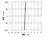
図1にアンドープp形リン化硼素層の表面に対向して設けたNi0.95B0.05合金からなる平面平行電極間の電流−電圧(I−V)特性を例示する。同図に例示する如く、低電圧及び低電流領域での印加電圧に対して電流が良好な直線性をもって変化する様は、Ni・B合金からは、p形リン化硼素系半導体について、オーミック接触性に優れるオーミック電極がもたらされることを明示している。 FIG. 1 illustrates current-voltage (IV) characteristics between plane parallel electrodes made of Ni 0.95 B 0.05 alloy provided facing the surface of an undoped p-type boron phosphide layer. As illustrated in the figure, from the Ni / B alloy, the p-type boron phosphide semiconductor is in ohmic contact so that the current changes with good linearity with respect to the applied voltage in the low voltage and low current regions. It is clearly shown that an ohmic electrode with excellent properties is provided.
本発明に係るp形オーミック電極は、要は、p形リン化硼素系半導体層に接触する部位がNi1-XBX合金から構成されていれば効果が発揮される。例えば、p形リン化硼素系半導体層に接する部位をNi0.80B0.20合金層とし、その上に中間層としてニッケル(Ni)層が配置され、更に、その上層として結線用途の金(Au)層を設けたNi0.80B0.20/Ni/Au3層重層構造電極を構成できる。重層構造のp形オーミック電極の中間層は、電極を構成する金属相互の拡散やp形リン化硼素系半導体をなすリン(P)等の構成元素の上層への拡散を低減するための機能層である。中間層は、Niの他、モリブデン(Mo)、タングステン(W)、白金(Pt)、チタン(Ti)等の高い融点の金属材料から構成できる。例えば、Ni0.90B0.10/Ti(中間層)/Al(上層)3層重層構成や、Ni0.98B0.02/Ti(中間層)/Pt(中間層)/Al(上層)4層重層構成からなるp形オーミック電極を例示できる。 In short, the p-type ohmic electrode according to the present invention is effective as long as the portion in contact with the p-type boron phosphide-based semiconductor layer is made of a Ni 1-X B X alloy. For example, a portion in contact with a p-type boron phosphide-based semiconductor layer is an Ni 0.80 B 0.20 alloy layer, a nickel (Ni) layer is disposed thereon as an intermediate layer, and a gold (Au) layer for connection use is further formed thereon. Ni 0.80 B 0.20 / Ni / Au three-layer multi-layer structure electrode can be constructed. The intermediate layer of the p-type ohmic electrode having a multilayer structure is a functional layer for reducing diffusion between metals constituting the electrode and diffusion of constituent elements such as phosphorus (P) constituting the p-type boron phosphide semiconductor into the upper layer. It is. The intermediate layer can be made of a metal material having a high melting point such as molybdenum (Mo), tungsten (W), platinum (Pt), titanium (Ti), etc. in addition to Ni. For example, it consists of a Ni 0.90 B 0.10 / Ti (intermediate layer) / Al (upper layer) three-layer structure, or a Ni 0.98 B 0.02 / Ti (intermediate layer) / Pt (intermediate layer) / Al (upper layer) four-layer structure. A p-type ohmic electrode can be exemplified.
p形オーミック電極を構成するためのNi1-XBX合金層は、通常のスパッタリング手段、鍍金(メッキ)手段等により形成できる。これらの手段において、p形リン化硼素系半導体層の表面を、公知のフォトリソグラフィー技術を駆使してパターニングを施したフォトレジスト材料で選択的に被覆しておけば、所望の形状のp形オーミック電極を形成できる。例えば、選択的にパターニングを施して、所望の位置に所望の形状に露出させたp形リン化硼素系半導体層の表面に、高周波スパッタ手段でNi1-XBX合金層を形成する。その後、レジスト材料をリフトオフ手段で剥離すれば、所望の形状の合金層を所望の位置に残置させられる。 The Ni 1-X B X alloy layer for constituting the p-type ohmic electrode can be formed by ordinary sputtering means, plating (plating) means or the like. In these means, if the surface of the p-type boron phosphide-based semiconductor layer is selectively covered with a photoresist material patterned using a known photolithography technique, a p-type ohmic having a desired shape is obtained. An electrode can be formed. For example, the Ni 1-X B X alloy layer is formed by high frequency sputtering means on the surface of the p-type boron phosphide-based semiconductor layer that is selectively patterned and exposed in a desired shape in a desired position. Thereafter, if the resist material is peeled off by lift-off means, an alloy layer having a desired shape can be left at a desired position.
p形リン化硼素系半導体層の表面の全体に、一旦、Ni1-XBX合金層を形成した後、公知のパターニング技術を利用しても所望の形状のp形オーミック電極を形成することができる。Ni1-XBX合金層からは、Ni単体から構成した場合に比較して、p形リン化硼素系半導体層との密着性に優れるオーミック電極を形成できる。このため、リフトオフ手段に依っても所望の外形のp形オーミック電極を形成するのに貢献できる。 A Ni 1-X B X alloy layer is once formed on the entire surface of the p-type boron phosphide-based semiconductor layer, and then a p-type ohmic electrode having a desired shape is formed using a known patterning technique. Can do. From the Ni 1-X B X alloy layer, an ohmic electrode having excellent adhesion to the p-type boron phosphide-based semiconductor layer can be formed as compared with a case where the Ni 1-X B X alloy layer is formed from Ni alone. For this reason, even if it depends on a lift-off means, it can contribute to forming the p-type ohmic electrode of a desired external shape.
p形オーミック電極は、種々の形状に形成することができる。一般的な円形や楕円形、また正方形や長方形などの方形となすことができる。また、LEDにあっては、p形オーミック電極を、p形リン化硼素系半導体層の表面の略全体に素子駆動電流を平面的に広範囲に亘り拡散できる形状とするのが好適である。例えば、櫛形状、格子状或いは網目状等とするのが好適である。p形リン化硼素層の表面に分散させて小型(小面積)のp形オーミック電極を配置した後、互いに孤立した小型の電極を互いに電気的に導通する、例えば、インジウム・錫複合酸化物(ITO)透明導電性電極を介して素子駆動電流を流通させても、素子駆動電流を拡散するのに効果を上げられる。この小型オーミック電極を分散させて設ける構成にあって、小型電極は一方でp形リン化硼素系半導体層に接し、他方で透明導電性電極に電気的に導通させて設ける必要がある。外部への発光の取り出し効率を向上させるために、小型オーミック電極を部分的に残存させたp形リン化硼素系半導体層に接触させて設けても構わない。 The p-type ohmic electrode can be formed in various shapes. It can be a general circle or ellipse, or a square such as a square or rectangle. In addition, in the LED, it is preferable that the p-type ohmic electrode has a shape capable of diffusing the element driving current over a wide range on a substantially entire surface of the p-type boron phosphide-based semiconductor layer. For example, a comb shape, a lattice shape, or a mesh shape is preferable. After disposing a small (small area) p-type ohmic electrode dispersed on the surface of the p-type boron phosphide layer, the small electrodes isolated from each other are electrically connected to each other. For example, indium-tin composite oxide ( Even if the element driving current is circulated through the ITO) transparent conductive electrode, it is effective to diffuse the element driving current. In the configuration in which the small ohmic electrodes are provided in a dispersed manner, the small electrodes need to be in contact with the p-type boron phosphide-based semiconductor layer on the one hand and electrically connected to the transparent conductive electrode on the other hand. In order to improve the efficiency of extracting light emitted to the outside, a small ohmic electrode may be provided in contact with the partially left p-type boron phosphide-based semiconductor layer.
所望の形状に加工した後、Ni1-XBX合金層にオーミック性を付与するための合金化(アロイング:alloying)熱処理を施す必要は必ずしもない。アロイ処理を敢えて施す場合は、アロイ温度はp形リン化硼素系半導体層の表面からのリンの脱離を防止するため、約500℃以下とするのが望ましい。アロイ雰囲気は、リンと揮発性物質を形成し易い水素(H2)よりも、窒素(N2)、アルゴン(Ar)等の不活性ガスが適する。アロイのための時間は、数分間から数10分間の範囲が適する。 After processing into a desired shape, it is not always necessary to perform an alloying heat treatment for imparting ohmic properties to the Ni 1-X B X alloy layer. When alloying is performed, the alloying temperature is preferably about 500 ° C. or lower in order to prevent phosphorus from detaching from the surface of the p-type boron phosphide-based semiconductor layer. In the alloy atmosphere, an inert gas such as nitrogen (N 2 ) or argon (Ar) is more suitable than hydrogen (H 2 ) that easily forms volatile substances with phosphorus. The time for the alloy is suitably in the range of several minutes to several tens of minutes.
p形リン化硼素系半導体層、特にアンドープの単量体のp形リン化硼素の表面に接触する様に設けた、ニッケルと硼素との合金膜は、p形リン化硼素系半導体層について良好なオーミック接触性をもたらす作用を有する。 A p-type boron phosphide-based semiconductor layer, particularly an alloy film of nickel and boron provided so as to be in contact with the surface of the undoped monomer p-type boron phosphide is good for the p-type boron phosphide-based semiconductor layer. Has the effect of providing a good ohmic contact.
p形リン化硼素系半導体層、特にアンドープの単量体のp形リン化硼素の表面に接触する様に設けた、硼素の重量含有率を25%以下とするニッケルと硼素との合金膜は、p形リン化硼素系半導体層について特に良好なオーミック接触性をもたらす作用を有する。 An alloy film of nickel and boron having a weight content of boron of 25% or less provided to be in contact with the surface of a p-type boron phosphide-based semiconductor layer, particularly p-type boron phosphide of an undoped monomer, The p-type boron phosphide-based semiconductor layer has an effect of providing particularly good ohmic contact.
p形リン化硼素半導体層の表面にニッケル・硼素(Ni・B)合金からなるp形オーミック電極を設けてリン化硼素半導体LEDを構成する場合を例にして本発明を具体的に説明する。 The present invention will be specifically described by taking as an example a case where a p-type ohmic electrode made of a nickel-boron (Ni.B) alloy is provided on the surface of a p-type boron phosphide semiconductor layer to constitute a boron phosphide semiconductor LED.
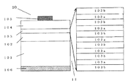
図2にダブルヘテロ(DH)接合構造のLED10を作製するために使用した積層構造体11の断面構造を模式的に示す。積層構造体11は、リン(P)ドープn形(111)−珪素(Si)単結晶基板101上に、アンドープでn形のリン化硼素(BP)からなる下部クラッド層102、n形窒化ガリウム・インジウム(Ga0.90In0.10N)井戸層103aと窒化ガリウム(GaN)障壁層103bとを5周期で重層させた多重量子井戸構造の発光層103、アンドープでp形のリン化硼素からなる上部クラッド層104を、順次、堆積して形成した。
FIG. 2 schematically shows a cross-sectional structure of the laminated structure 11 used for manufacturing the
アンドープのn形及びp形リン化硼素層102,104は、トリエチル硼素(分子式:(C2H5)3B)を硼素(B)源とし、ホスフィン(分子式:PH3)をリン源とする常圧(略大気圧)有機金属気相エピタキシー(MOVPE)手段を利用して形成した。n形リン化硼素層102は925℃で、p形リン化硼素層104は1025℃で、V/III比率(=PH3/(C2H5)3B供給濃度比率)を10として形成した。発光層103は、トリメチルガリウム(分子式:(CH3)3Ga)/NH3/H2反応系常圧MOCVD手段により、800℃で形成した。井戸層103aを構成する上記の窒化ガリウム・インジウム層は、インジウム組成を相違する複数の相から構成される多相構造から構成し、その平均的なインジウム組成は0.10(=10%)であった。井戸層103a及び障壁層103bの層厚は、各々、5nm及び10nmとした。
The undoped n-type and p-type boron phosphide layers 102 and 104 use triethylboron (molecular formula: (C 2 H 5 ) 3 B) as a boron (B) source and phosphine (molecular formula: PH 3 ) as a phosphorus source. It was formed using an atmospheric pressure (substantially atmospheric pressure) organometallic vapor phase epitaxy (MOVPE) means. The n-type
上部クラッド層104をなすアンドープのp形リン化硼素層104のキャリア(正孔)濃度は2×1019cm-3とし、層厚は720nmとした。同層104の室温での抵抗率は5×10⁻²Ω・cmであった。また、p形リン化硼素層104の室温での禁止帯幅は3.2eVであったため、発光層103からの発光を外部へ透過するための窓層を兼用するp形クラッド層として利用した。
The undoped p-type
p形上部クラッド層をなすp形リン化硼素層104の表面の全面に、通常の高周波スパッタリング法及び電子ビーム蒸着法に依り、ニッケル・硼素(Ni0.75B0.25)合金膜、チタン(Ti)膜、及び金(Au)膜を順次、被着させた。次に、結線用の台座電極を兼ねるp形オーミック電極105を設ける領域に限り、底面部をNi0.75B0.25合金膜とする上記の3層重層電極を残置させるために、公知のフォトリソグラフィー技術を利用して選択的にパターニングを施した。次に、一般的な高周波プラズマエッチング手段に依りp形台座電極105とする以外の領域に在るNi0.75B0.25合金膜をエッチングして除去し、p形リン化硼素層104の表面を露出させた。
A nickel-boron (Ni 0.75 B 0.25 ) alloy film and a titanium (Ti) film are formed on the entire surface of the p-type
フォトレジスト材を剥離した後、再び、チップに裁断するための格子状の溝を設けるために選択的パターニングを施した。然る後、塩素を含むハロゲン系混合ガスを利用したプラズマドライエッチング手法に依り、上記のパターニングを施した領域に限定して、p形リン化硼素層104を選択的にエッチングで除去し、裁断用の溝を形成した。
After peeling off the photoresist material, selective patterning was performed again to provide a grid-like groove for cutting into chips. Thereafter, the p-type
一方、珪素単結晶基板101の裏面の全面には、一般の真空蒸着法に依り金(Au)膜を被着させてn形オーミック電極(負電極)106を形成した。Si単結晶基板101の(111)−結晶表面に直交する<110>結晶方位に平行に設けた、線幅を50μmとする上記の帯状の溝に沿って劈開し、一辺を350μmとする正方形のLEDチップ10とした。
On the other hand, an n-type ohmic electrode (negative electrode) 106 was formed on the entire back surface of the silicon single crystal substrate 101 by depositing a gold (Au) film by a general vacuum deposition method. A square shape having a side width of 350 μm, cleaved along the above-mentioned strip-shaped groove having a line width of 50 μm provided in parallel to the <110> crystal orientation orthogonal to the (111) -crystal surface of the Si single crystal substrate 101
本発明では、p形オーミック電極105の底面部を、上部クラッド層104をなすp形リン化硼素層との密着性に優れるニッケル・硼素(Ni・B)合金膜から構成したため、結線時に於いても、p形リン化硼素層104から剥離しない台座電極を兼ねるp形オーミック電極105とすることができた。また、p形オーミック電極105の底面部を、p形リン化硼素層に対して特に、小さな接触抵抗を与えるNi・B合金膜から構成したため、順方向電流を20mAとした際の順方向電圧(Vf)は3.1Vと低値となった。一方、逆方向電流を10μAとした際の逆方向電圧は9.5Vと高値となった。
In the present invention, the bottom surface of the p-
p形及びn形オーミック電極105、106の間に、順方向に20mAの素子駆動電流を流通してLEDチップ10の発光特性を確認した。LED10からは中心の波長を440nmとする青色帯光が放射された。発光スペクトルの半値幅は210ミリエレクトロンボルト(単位:meV)であった。また、高いキャリア濃度で低抵抗のアンドープp形リン化硼素層から上部クラッド層を構成することとし、且つ、アンドープのp形リン化硼素の表面に接触させて低接触抵抗のNi・B合金膜を含むp形オーミック電極を設けることとしたので、素子駆動電流を台座電極の射影領域以外の発光領域に充分に拡散でき、発光層の略全面から発光がもたらされた。このため、一般的な積分球を利用して測定される樹脂モールド以前のチップ状態での輝度は11ミリカンデラ(mcd)に達した。
Between the p-type and n-
10 LEDチップ
11 積層構造体
101 珪素単結晶基板
102 下部クラッド層(n形リン化硼素層)
103 発光層
103a 井戸層
103b 障壁層
104 上部クラッド層(p形リン化硼素層)
105 p形オーミック電極(p形台座電極)
106 n形オーミック電極
10 LED chip 11 Laminated structure 101 Silicon
103 light emitting layer 103a well layer 103b
105 p-type ohmic electrode (p-type pedestal electrode)
106 n-type ohmic electrode
Claims (3)
上記p形オーミック電極を、ニッケルと硼素との合金から構成した、ことを特徴とするリン化硼素系半導体素子。 In a boron phosphide-based semiconductor element comprising at least a p-type boron phosphide-based semiconductor layer and a p-type ohmic electrode formed thereon,
A boron phosphide-based semiconductor element, wherein the p-type ohmic electrode is made of an alloy of nickel and boron.
Priority Applications (1)
| Application Number | Priority Date | Filing Date | Title |
|---|---|---|---|
| JP2005061866A JP4658643B2 (en) | 2004-03-08 | 2005-03-07 | Boron phosphide semiconductor device |
Applications Claiming Priority (2)
| Application Number | Priority Date | Filing Date | Title |
|---|---|---|---|
| JP2004063749 | 2004-03-08 | ||
| JP2005061866A JP4658643B2 (en) | 2004-03-08 | 2005-03-07 | Boron phosphide semiconductor device |
Publications (2)
| Publication Number | Publication Date |
|---|---|
| JP2005294812A true JP2005294812A (en) | 2005-10-20 |
| JP4658643B2 JP4658643B2 (en) | 2011-03-23 |
Family
ID=35327348
Family Applications (1)
| Application Number | Title | Priority Date | Filing Date |
|---|---|---|---|
| JP2005061866A Expired - Fee Related JP4658643B2 (en) | 2004-03-08 | 2005-03-07 | Boron phosphide semiconductor device |
Country Status (1)
| Country | Link |
|---|---|
| JP (1) | JP4658643B2 (en) |
Citations (3)
| Publication number | Priority date | Publication date | Assignee | Title |
|---|---|---|---|---|
| US3054936A (en) * | 1959-10-16 | 1962-09-18 | Monsanto Chemicals | Transistor |
| JPH05102066A (en) * | 1991-10-04 | 1993-04-23 | Fujitsu Ltd | Manufacture of semiconductor element |
| JP2000101139A (en) * | 1998-09-25 | 2000-04-07 | Toshiba Corp | Semiconductor light emitting element, method of manufacturing the same, and semiconductor light emitting device |
-
2005
- 2005-03-07 JP JP2005061866A patent/JP4658643B2/en not_active Expired - Fee Related
Patent Citations (3)
| Publication number | Priority date | Publication date | Assignee | Title |
|---|---|---|---|---|
| US3054936A (en) * | 1959-10-16 | 1962-09-18 | Monsanto Chemicals | Transistor |
| JPH05102066A (en) * | 1991-10-04 | 1993-04-23 | Fujitsu Ltd | Manufacture of semiconductor element |
| JP2000101139A (en) * | 1998-09-25 | 2000-04-07 | Toshiba Corp | Semiconductor light emitting element, method of manufacturing the same, and semiconductor light emitting device |
Also Published As
| Publication number | Publication date |
|---|---|
| JP4658643B2 (en) | 2011-03-23 |
Similar Documents
| Publication | Publication Date | Title |
|---|---|---|
| JP4023121B2 (en) | N-type electrode, group III nitride compound semiconductor device, method for manufacturing n-type electrode, and method for manufacturing group III nitride compound semiconductor device | |
| CN102246326B (en) | Semiconductor light emission element | |
| JP2005244207A (en) | Gallium nitride compound semiconductor light emitting device | |
| JP3567926B2 (en) | pn junction type boron phosphide-based semiconductor light emitting device, method for manufacturing the same, and light source for display device | |
| JP4063801B2 (en) | Light emitting diode | |
| JP4439400B2 (en) | Boron phosphide-based semiconductor light emitting device, manufacturing method thereof, and light emitting diode | |
| JP3724267B2 (en) | Group III nitride semiconductor light emitting device | |
| JP2001077414A (en) | Group iii nitride semiconductor light-emitting diode | |
| JP2000353820A (en) | AlGaInP LIGHT EMITTING ELEMENT WITH WINDOW LAYER | |
| JP2003124518A (en) | Gallium nitride based semiconductor light emitting device and method of manufacturing the same | |
| US7538361B2 (en) | Ohmic electrode structure, compound semiconductor light emitting device having the same, and LED lamp | |
| JPH10308533A (en) | Gallium nitride based compound semiconductor light emitting device, method of manufacturing the same, and light emitting device | |
| JP4658643B2 (en) | Boron phosphide semiconductor device | |
| JP4030534B2 (en) | Compound semiconductor light emitting device and manufacturing method thereof | |
| JP4030513B2 (en) | Ohmic electrode structure, compound semiconductor light emitting device and LED lamp provided with the same | |
| CN100413106C (en) | Compound semiconductor light emitting device | |
| CN1934717B (en) | Compound semiconductor light-emitting diode | |
| JP4039187B2 (en) | Semiconductor light emitting device | |
| JP4502691B2 (en) | P-type ohmic electrode structure, compound semiconductor light emitting device and LED lamp having the same | |
| JP2002246645A (en) | Group iii nitride semiconductor light emitting diode | |
| JP4376361B2 (en) | AlGaInP light emitting diode | |
| KR100638148B1 (en) | Boron phosphide-based semiconductor light-emitting device and production method thereof | |
| TWI251944B (en) | Resistance electrode structure, compound semiconductor light emitting device having the same, and LED lamp | |
| JP4518881B2 (en) | P-type ohmic electrode, compound semiconductor device including the same, compound semiconductor light-emitting device, and manufacturing method thereof | |
| JP4757514B2 (en) | Compound semiconductor light emitting diode |
Legal Events
| Date | Code | Title | Description |
|---|---|---|---|
| A621 | Written request for application examination |
Free format text: JAPANESE INTERMEDIATE CODE: A621 Effective date: 20080107 |
|
| A977 | Report on retrieval |
Free format text: JAPANESE INTERMEDIATE CODE: A971007 Effective date: 20100615 |
|
| A131 | Notification of reasons for refusal |
Free format text: JAPANESE INTERMEDIATE CODE: A131 Effective date: 20100622 |
|
| A521 | Written amendment |
Free format text: JAPANESE INTERMEDIATE CODE: A523 Effective date: 20100820 |
|
| TRDD | Decision of grant or rejection written | ||
| A01 | Written decision to grant a patent or to grant a registration (utility model) |
Free format text: JAPANESE INTERMEDIATE CODE: A01 Effective date: 20101221 |
|
| A01 | Written decision to grant a patent or to grant a registration (utility model) |
Free format text: JAPANESE INTERMEDIATE CODE: A01 |
|
| A61 | First payment of annual fees (during grant procedure) |
Free format text: JAPANESE INTERMEDIATE CODE: A61 Effective date: 20101224 |
|
| FPAY | Renewal fee payment (prs date is renewal date of database) |
Free format text: PAYMENT UNTIL: 20140107 Year of fee payment: 3 |
|
| R150 | Certificate of patent (=grant) or registration of utility model |
Free format text: JAPANESE INTERMEDIATE CODE: R150 |
|
| LAPS | Cancellation because of no payment of annual fees |