JP2005294785A - Organic semiconductor device - Google Patents
Organic semiconductor device Download PDFInfo
- Publication number
- JP2005294785A JP2005294785A JP2004134881A JP2004134881A JP2005294785A JP 2005294785 A JP2005294785 A JP 2005294785A JP 2004134881 A JP2004134881 A JP 2004134881A JP 2004134881 A JP2004134881 A JP 2004134881A JP 2005294785 A JP2005294785 A JP 2005294785A
- Authority
- JP
- Japan
- Prior art keywords
- organic semiconductor
- electrode
- semiconductor device
- layer
- organic
- Prior art date
- Legal status (The legal status is an assumption and is not a legal conclusion. Google has not performed a legal analysis and makes no representation as to the accuracy of the status listed.)
- Granted
Links
Images

Classifications
-
- H—ELECTRICITY
- H10—SEMICONDUCTOR DEVICES; ELECTRIC SOLID-STATE DEVICES NOT OTHERWISE PROVIDED FOR
- H10K—ORGANIC ELECTRIC SOLID-STATE DEVICES
- H10K85/00—Organic materials used in the body or electrodes of devices covered by this subclass
- H10K85/60—Organic compounds having low molecular weight
- H10K85/649—Aromatic compounds comprising a hetero atom
- H10K85/657—Polycyclic condensed heteroaromatic hydrocarbons
-
- H—ELECTRICITY
- H10—SEMICONDUCTOR DEVICES; ELECTRIC SOLID-STATE DEVICES NOT OTHERWISE PROVIDED FOR
- H10K—ORGANIC ELECTRIC SOLID-STATE DEVICES
- H10K10/00—Organic devices specially adapted for rectifying, amplifying, oscillating or switching; Organic capacitors or resistors having potential barriers
- H10K10/40—Organic transistors
- H10K10/46—Field-effect transistors, e.g. organic thin-film transistors [OTFT]
- H10K10/462—Insulated gate field-effect transistors [IGFETs]
- H10K10/484—Insulated gate field-effect transistors [IGFETs] characterised by the channel regions
-
- H—ELECTRICITY
- H10—SEMICONDUCTOR DEVICES; ELECTRIC SOLID-STATE DEVICES NOT OTHERWISE PROVIDED FOR
- H10K—ORGANIC ELECTRIC SOLID-STATE DEVICES
- H10K10/00—Organic devices specially adapted for rectifying, amplifying, oscillating or switching; Organic capacitors or resistors having potential barriers
- H10K10/80—Constructional details
- H10K10/82—Electrodes
- H10K10/84—Ohmic electrodes, e.g. source or drain electrodes
-
- H—ELECTRICITY
- H10—SEMICONDUCTOR DEVICES; ELECTRIC SOLID-STATE DEVICES NOT OTHERWISE PROVIDED FOR
- H10K—ORGANIC ELECTRIC SOLID-STATE DEVICES
- H10K85/00—Organic materials used in the body or electrodes of devices covered by this subclass
- H10K85/60—Organic compounds having low molecular weight
- H10K85/615—Polycyclic condensed aromatic hydrocarbons, e.g. anthracene
-
- H—ELECTRICITY
- H10—SEMICONDUCTOR DEVICES; ELECTRIC SOLID-STATE DEVICES NOT OTHERWISE PROVIDED FOR
- H10K—ORGANIC ELECTRIC SOLID-STATE DEVICES
- H10K85/00—Organic materials used in the body or electrodes of devices covered by this subclass
- H10K85/731—Liquid crystalline materials
-
- H—ELECTRICITY
- H10—SEMICONDUCTOR DEVICES; ELECTRIC SOLID-STATE DEVICES NOT OTHERWISE PROVIDED FOR
- H10K—ORGANIC ELECTRIC SOLID-STATE DEVICES
- H10K10/00—Organic devices specially adapted for rectifying, amplifying, oscillating or switching; Organic capacitors or resistors having potential barriers
- H10K10/40—Organic transistors
- H10K10/46—Field-effect transistors, e.g. organic thin-film transistors [OTFT]
- H10K10/462—Insulated gate field-effect transistors [IGFETs]
- H10K10/464—Lateral top-gate IGFETs comprising only a single gate
-
- H—ELECTRICITY
- H10—SEMICONDUCTOR DEVICES; ELECTRIC SOLID-STATE DEVICES NOT OTHERWISE PROVIDED FOR
- H10K—ORGANIC ELECTRIC SOLID-STATE DEVICES
- H10K10/00—Organic devices specially adapted for rectifying, amplifying, oscillating or switching; Organic capacitors or resistors having potential barriers
- H10K10/40—Organic transistors
- H10K10/46—Field-effect transistors, e.g. organic thin-film transistors [OTFT]
- H10K10/462—Insulated gate field-effect transistors [IGFETs]
- H10K10/466—Lateral bottom-gate IGFETs comprising only a single gate
-
- H—ELECTRICITY
- H10—SEMICONDUCTOR DEVICES; ELECTRIC SOLID-STATE DEVICES NOT OTHERWISE PROVIDED FOR
- H10K—ORGANIC ELECTRIC SOLID-STATE DEVICES
- H10K85/00—Organic materials used in the body or electrodes of devices covered by this subclass
- H10K85/60—Organic compounds having low molecular weight
- H10K85/649—Aromatic compounds comprising a hetero atom
- H10K85/653—Aromatic compounds comprising a hetero atom comprising only oxygen as heteroatom
-
- H—ELECTRICITY
- H10—SEMICONDUCTOR DEVICES; ELECTRIC SOLID-STATE DEVICES NOT OTHERWISE PROVIDED FOR
- H10K—ORGANIC ELECTRIC SOLID-STATE DEVICES
- H10K85/00—Organic materials used in the body or electrodes of devices covered by this subclass
- H10K85/60—Organic compounds having low molecular weight
- H10K85/649—Aromatic compounds comprising a hetero atom
- H10K85/654—Aromatic compounds comprising a hetero atom comprising only nitrogen as heteroatom
-
- H—ELECTRICITY
- H10—SEMICONDUCTOR DEVICES; ELECTRIC SOLID-STATE DEVICES NOT OTHERWISE PROVIDED FOR
- H10K—ORGANIC ELECTRIC SOLID-STATE DEVICES
- H10K85/00—Organic materials used in the body or electrodes of devices covered by this subclass
- H10K85/60—Organic compounds having low molecular weight
- H10K85/649—Aromatic compounds comprising a hetero atom
- H10K85/655—Aromatic compounds comprising a hetero atom comprising only sulfur as heteroatom
Landscapes
- Chemical & Material Sciences (AREA)
- Engineering & Computer Science (AREA)
- Materials Engineering (AREA)
- Physics & Mathematics (AREA)
- Spectroscopy & Molecular Physics (AREA)
- Crystallography & Structural Chemistry (AREA)
- Thin Film Transistor (AREA)
- Electroluminescent Light Sources (AREA)
Abstract
【課題】 有機半導体層への電荷注入が容易で、電荷移動特性のよい有機半導体層を備えた有機半導体装置を提供する。
【解決手段】 対向する第1の電極及び第2の電極と、第1の電極及び第2の電極の間に設けられた有機半導体層とを有する有機半導体装置であって、第1の電極及び第2の電極のうち少なくとも一方の電極と有機半導体層との間に、電荷注入促進層が形成されている有機半導体装置により、上記課題を解決した。
【選択図】 図1PROBLEM TO BE SOLVED: To provide an organic semiconductor device provided with an organic semiconductor layer which can easily inject charges into the organic semiconductor layer and has good charge transfer characteristics.
An organic semiconductor device having opposing first and second electrodes and an organic semiconductor layer provided between the first electrode and the second electrode, the first electrode and The above problems have been solved by an organic semiconductor device in which a charge injection promoting layer is formed between at least one of the second electrodes and the organic semiconductor layer.
[Selection] Figure 1
Description
本発明は、有機半導体装置に関し、更に詳しくは、電荷移動度に優れた液晶性有機半導体材料を含む有機半導体層を有する有機半導体装置に関するものである。 The present invention relates to an organic semiconductor device, and more particularly to an organic semiconductor device having an organic semiconductor layer containing a liquid crystalline organic semiconductor material having excellent charge mobility.
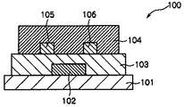
図8は、従来の有機半導体装置の一例を示す断面図である。従来の有機半導体装置100は、基板101、ゲート電極102、ゲート絶縁層103、有機半導体層104、ソース電極105及びドレイン電極106で構成されている。こうした構成からなる有機半導体装置においては、有機半導体層が十分な電荷移動度を有することが要求されており、近年電荷移動度の高い有機半導体材料についての研究がなされている。 FIG. 8 is a cross-sectional view showing an example of a conventional organic semiconductor device. A conventional
高い電荷移動度を有する材料としては液晶性有機半導体材料が知られており、例えばHaarerらにより、代表的なディスコティック液晶である長鎖トリフェニレン系化合物のメゾフェーズにおいて10−1cm2/V・sという高速な正孔の移動度を示すことが報告され(例えば、非特許文献1を参照。)、半那らにより、フェニルナフタレン骨格を有する棒状液晶がスメクティックE(SmE)相が10−2cm2/V・sという高い電荷移動度を示すことが報告されている(例えば、非特許文献2を参照。)。これらの液晶性有機半導体材料は、有機半導体素子用のチャネル領域を構成する成膜材料として期待されている。
上述したような電荷移動度の高い有機半導体層においては、その前提として有機半導体層に充分な量の電荷(正孔、電子)が効率的かつ速やかに供給(注入)されることが必要である。しかし、電荷を供給するソース電極と有機半導体層とはエネルギーギャップが大きいので、有機半導体層に電荷が容易に注入されないという問題がある。 In the organic semiconductor layer having a high charge mobility as described above, it is necessary to supply (inject) a sufficient amount of charges (holes, electrons) efficiently and promptly to the organic semiconductor layer as a precondition. . However, since the energy gap between the source electrode for supplying charges and the organic semiconductor layer is large, there is a problem that charges are not easily injected into the organic semiconductor layer.
ところで、有機エレクトロルミネセンス(以下、有機ELという。)の分野では、上記特許文献1に示したように、陽極の発光層側の表面に電気二重層の効果を持つ双極子モーメントを有する有機薄膜が正孔注入促進層として形成された有機EL素子が報告されている。この報告には、その双極子モーメントを有する有機薄膜の作用により電極と発光層とのエネルギーギャップを小さくして陽極から発光層への正孔注入を容易にし、駆動電圧の低電圧化を達成できると記載されている。また、上記特許文献2に示したように、陽極の発光層側の表面にπ電子系等の官能基を有した双極子化合物からなる有機薄膜が正孔注入促進層として形成された有機EL素子が報告されている。この報告には、その有機薄膜が電極と発光層とのエネルギーギャップを小さくする電気二重層として作用して、電極から発光層への電荷の注入を容易にすることが記載されている。 By the way, in the field of organic electroluminescence (hereinafter referred to as organic EL), as shown in Patent Document 1, an organic thin film having a dipole moment having an electric double layer effect on the surface of the anode on the light emitting layer side. Has been reported as an organic EL device in which is formed as a hole injection promoting layer. In this report, the action of the organic thin film having the dipole moment reduces the energy gap between the electrode and the light-emitting layer, facilitates hole injection from the anode to the light-emitting layer, and achieves a low driving voltage. It is described. Further, as shown in Patent Document 2, an organic EL element in which an organic thin film made of a dipole compound having a functional group such as a π-electron system is formed as a hole injection promoting layer on the surface of the anode on the light emitting layer side Has been reported. This report describes that the organic thin film acts as an electric double layer that reduces the energy gap between the electrode and the light emitting layer, facilitating injection of charges from the electrode to the light emitting layer.
本発明は、有機半導体装置における上述した問題を解決するためになされたものであって、その目的は、有機半導体層への電荷注入が容易で、電荷移動特性のよい有機半導体層を備えた有機半導体装置を提供することにある。 The present invention has been made to solve the above-described problems in organic semiconductor devices, and an object of the present invention is to provide an organic semiconductor layer having an organic semiconductor layer that facilitates charge injection into the organic semiconductor layer and has good charge transfer characteristics. It is to provide a semiconductor device.
上記課題を解決するための本発明の有機半導体装置は、対向する第1の電極及び第2の電極と、当該第1の電極及び当該第2の電極の間に設けられた有機半導体層とを有する有機半導体装置であって、前記第1の電極及び前記第2の電極のうち少なくとも一方の電極と前記有機半導体層との間に、電荷注入促進層が形成されていることを特徴とする。 An organic semiconductor device of the present invention for solving the above problems includes a first electrode and a second electrode facing each other, and an organic semiconductor layer provided between the first electrode and the second electrode. An organic semiconductor device having a charge injection promoting layer formed between at least one of the first electrode and the second electrode and the organic semiconductor layer.
この発明によれば、第1の電極及び第2の電極のうち少なくとも一方と有機半導体層との間に電荷注入促進層を形成したので、電荷注入促進層の作用により有機半導体層への電荷の注入が容易となる。 According to the present invention, the charge injection promoting layer is formed between at least one of the first electrode and the second electrode and the organic semiconductor layer. Injection is easy.
本発明の有機半導体装置において、前記有機半導体層が液晶性有機半導体材料で形成されていることが好ましい。 In the organic semiconductor device of the present invention, it is preferable that the organic semiconductor layer is formed of a liquid crystalline organic semiconductor material.
この発明によれば、有機半導体層が液晶性有機半導体材料で形成されているので、電荷移動度のよい有機半導体層の形成が可能となる。 According to this invention, since the organic semiconductor layer is formed of a liquid crystalline organic semiconductor material, it is possible to form an organic semiconductor layer with good charge mobility.
本発明の有機半導体装置において、前記液晶性有機半導体材料が下記化学式1で表される液晶性分子からなることが好ましい。 In the organic semiconductor device of the present invention, the liquid crystalline organic semiconductor material is preferably composed of a liquid crystalline molecule represented by the following chemical formula 1.
![]()
![]()
(式中Aは、L個の6π電子系環、M個の8π電子系環、N個の10π電子系環、O個の12π電子系環、P個の14π電子系環、Q個の16π電子系環、R個の18π電子系環、S個の20π電子系環、T個の22π電子系環、U個の24π電子系環、V個の26π電子系環(但し、L,M,N,O,P,Q,R,S,T,U及びVは、それぞれ0〜12の整数を表し、L+M+N+O+P+Q+R+S+T+U+V=1〜12とする。)を含む骨格構造を有するコア部位を表す。また、式中B及びB’は、屈曲性の高い鎖状構造、又は、水素若しくはハロゲン等の官能基を表す。) (Where A is L 6π electron ring, M 8π electron ring, N 10π electron ring, O 12π electron ring, P 14π electron ring, Q 16π electron ring, Q 16π electron ring) Electron ring, R 18π electron ring, S 20π electron ring, T 22π electron ring, U 24π electron ring, V 26π electron ring (provided that L, M, N, O, P, Q, R, S, T, U, and V each represents an integer of 0 to 12, and represents a core portion having a skeleton structure including L + M + N + O + P + Q + R + S + T + U + V = 1-12. In the formula, B and B ′ represent a highly flexible chain structure or a functional group such as hydrogen or halogen.)
この発明において、液晶性分子は、その骨格構造が隣接するように存在し、その鎖状分子が隣接するように存在するので、骨格構造が隣接する領域は、高い自己組織性を有した分子凝集部分となっている。その結果、その分子凝集部分では、電子や正孔がホッピング伝導を起こし易いので、このような液晶性分子を有する液晶性有機半導体材料で形成された有機半導体層は高い電荷移動度を有する。 In this invention, the liquid crystalline molecules exist so that their skeleton structures are adjacent to each other, and the chain molecules are adjacent to each other. Therefore, the regions where the skeleton structures are adjacent to each other are molecular aggregates having high self-organization. It has become a part. As a result, since electrons and holes easily cause hopping conduction in the molecular aggregation portion, an organic semiconductor layer formed of a liquid crystalline organic semiconductor material having such a liquid crystalline molecule has high charge mobility.
本発明の有機半導体装置において、前記液晶性有機半導体材料が、サーモトロピック液晶相状態及びリオトロピック液晶相状態のうち少なくとも一方を有することが好ましい。 In the organic semiconductor device of the present invention, it is preferable that the liquid crystalline organic semiconductor material has at least one of a thermotropic liquid crystal phase state and a lyotropic liquid crystal phase state.
本発明の有機半導体装置において、前記サーモトロピック液晶相状態がスメクティック液晶相状態であることが好ましい。 In the organic semiconductor device of the present invention, it is preferable that the thermotropic liquid crystal phase state is a smectic liquid crystal phase state.
本発明の有機半導体装置において、前記有機半導体層が、10−6cm2/V・s以上の電荷移動度を示すことが好ましい。In the organic semiconductor device of the present invention, the organic semiconductor layer preferably exhibits a charge mobility of 10 −6 cm 2 / V · s or more.
本発明の有機半導体装置において、前記電荷注入促進層が双極子モーメントを有する有機薄膜であることが好ましい。 In the organic semiconductor device of the present invention, the charge injection promoting layer is preferably an organic thin film having a dipole moment.
この発明によれば、前記電荷注入促進層が双極子モーメントを有する有機薄膜であるので、電極の仕事関数と有機半導体層の仕事関数との差を小さくすることができる(すなわち両者の間に存在する電荷注入障壁を小さくすることができる)。その結果、その有機薄膜の作用により有機半導体層への電荷の注入が容易となる。 According to this invention, since the charge injection promoting layer is an organic thin film having a dipole moment, the difference between the work function of the electrode and the work function of the organic semiconductor layer can be reduced (that is, between the two). The charge injection barrier can be reduced). As a result, charge injection into the organic semiconductor layer is facilitated by the action of the organic thin film.
本発明の有機半導体装置において、(A)前記電荷注入促進層が、絶対値で1デバイ以上50デバイ以下の間に絶対値を持つベクトルで表される電気双極子モーメントを有する有機化合物で形成されており、前記ベクトルの向きは、前記有機化合物の正極が前記第1の電極及び前記第2の電極のうち正孔を注入する電極側に位置し、前記有機化合物の負極が前記有機半導体層側に位置することになる向きであること、(B)前記電荷注入促進層が、絶対値で1デバイ以上50デバイ以下の間に絶対値を持つベクトルで表される電気双極子モーメントを有する有機化合物で形成されており、前記ベクトルの向きは、前記有機化合物の負極が前記第1の電極及び前記第2の電極のうち電子を注入する電極側に位置し、前記有機化合物の正極が前記有機半導体層側に位置することになる向きであること、が好ましい。 In the organic semiconductor device of the present invention, (A) the charge injection promoting layer is formed of an organic compound having an electric dipole moment represented by a vector having an absolute value between 1 debye and 50 debye in absolute value. The positive direction of the organic compound is positioned on the side of the first electrode and the second electrode that injects holes, and the negative direction of the organic compound is on the organic semiconductor layer side. (B) the organic compound in which the charge injection promoting layer has an electric dipole moment represented by a vector having an absolute value between 1 debye and 50 debye in absolute value The organic compound negative electrode is positioned on the electrode side for injecting electrons of the first electrode and the second electrode, and the organic compound positive electrode is It is the orientation will be positioned to the machine the semiconductor layer side, is preferred.
これらの発明によれば、電荷を注入する電極に上記の電気双極子モーメントを有する有機化合物が化学的に結合することにより双極子モーメントを有する有機薄膜(電荷注入促進層)が形成されるので、そのような電極から有機半導体層への電荷の注入を容易に促進させることができる。 According to these inventions, an organic thin film having a dipole moment (charge injection promoting layer) is formed by chemically bonding the organic compound having the electric dipole moment to the electrode for injecting charges. Charge injection from such an electrode into the organic semiconductor layer can be facilitated.
本発明の有機半導体装置において、前記電荷注入促進層が下記の化学式44に示す有機化合物及び下記の化学式46に示す有機化合物のいずれか一方からなる有機薄膜であることが好ましい。 In the organic semiconductor device of the present invention, the charge injection promoting layer is preferably an organic thin film made of one of an organic compound represented by the following chemical formula 44 and an organic compound represented by the following chemical formula 46.
![]()
![]()
![]()
![]()
(式44及び式46中、Arは芳香族炭化水素環又は芳香族複素環を表す、Yは及びY’は電極若しくは電極近傍に存在する反応性基との連結基を表す、X及びX’は置換基を表す。) (In the formulas 44 and 46, Ar represents an aromatic hydrocarbon ring or an aromatic heterocyclic ring, Y represents Y and Y ′ represents a linking group with an electrode or a reactive group present in the vicinity of the electrode, and X and X ′. Represents a substituent.)
本発明の有機半導体装置において、前記第1の電極がソース電極であり、前記第2の電極がドレイン電極であり、前記有機半導体層が前記ソース電極及び前記ドレイン電極の間のチャネル領域に形成されており、基板、ゲート電極及びゲート絶縁層を更に有することが好ましい。 In the organic semiconductor device of the present invention, the first electrode is a source electrode, the second electrode is a drain electrode, and the organic semiconductor layer is formed in a channel region between the source electrode and the drain electrode. It is preferable to further include a substrate, a gate electrode, and a gate insulating layer.
本発明の有機半導体装置において、前記基板上に前記ソース電極及び前記ドレイン電極が形成されており、前記電荷注入促進層が、前記ソース電極及び前記ドレイン電極の少なくとも一方の電極上、又は、前記ソース電極及び前記ドレイン電極の少なくとも一方の電極の近傍の前記チャネル領域内に形成されていることが好ましい。 In the organic semiconductor device of the present invention, the source electrode and the drain electrode are formed on the substrate, and the charge injection promoting layer is formed on at least one of the source electrode and the drain electrode or the source. Preferably, it is formed in the channel region in the vicinity of at least one of the electrode and the drain electrode.
本発明の有機半導体装置において、前記基板は前記ソース電極が形成された第1の電極基板であり、前記ドレイン電極が形成された第2の電極基板を更に備え、前記第1の電極基板と前記第2の電極基板とが対向して設けられており、前記電荷注入促進層が、前記ソース電極及び前記ドレイン電極の少なくとも一方の電極上、又は、前記ソース電極及び前記ドレイン電極の少なくとも一方の電極の近傍の前記チャネル領域内に形成されていることが好ましい。 In the organic semiconductor device of the present invention, the substrate is a first electrode substrate on which the source electrode is formed, and further includes a second electrode substrate on which the drain electrode is formed, the first electrode substrate and the A charge injection promoting layer is provided on at least one of the source electrode and the drain electrode or at least one electrode of the source electrode and the drain electrode. Is preferably formed in the channel region in the vicinity of.
本発明の有機半導体装置によれば、互いに対向した第1の電極及び第2の電極のうち少なくとも一方の電極と有機半導体層との間に電荷注入促進層が設けられているので、有機半導体層への電荷の注入が容易となる。その結果、電荷移動に充分な量の電荷が有機半導体層に効率的かつ速やかに供給される。特に、液晶性有機半導体材料により形成された有機半導体層には充分な量の電荷が供給されるので、そのような有機半導体層を有する有機半導体装置は、多くの電荷を高速で移動させることができる。 According to the organic semiconductor device of the present invention, since the charge injection promoting layer is provided between at least one of the first electrode and the second electrode facing each other and the organic semiconductor layer, the organic semiconductor layer It becomes easy to inject charges into As a result, a sufficient amount of charge for charge transfer is efficiently and rapidly supplied to the organic semiconductor layer. In particular, since a sufficient amount of charge is supplied to an organic semiconductor layer formed of a liquid crystalline organic semiconductor material, an organic semiconductor device having such an organic semiconductor layer can move a large amount of charge at high speed. it can.
本発明の有機半導体装置は、対向する第1の電極及び第2の電極と、前記第1の電極及び前記第2の電極の間に設けられた有機半導体層とを有し、前記第1の電極及び前記第2の電極のうち少なくとも一方と前記有機半導体層との間には電荷注入促進層が形成されている。 The organic semiconductor device of the present invention includes a first electrode and a second electrode facing each other, and an organic semiconductor layer provided between the first electrode and the second electrode. A charge injection promoting layer is formed between at least one of the electrode and the second electrode and the organic semiconductor layer.
以下、本発明の有機半導体装置を、有機トランジスタ素子を例にして詳しく説明する。 Hereinafter, the organic semiconductor device of the present invention will be described in detail using an organic transistor element as an example.
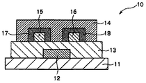
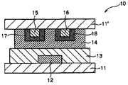
図1は、本発明の有機半導体装置(有機トランジスタ素子)の層構成の一例を示す断面模式図である。本発明の有機半導体装置(有機トランジスタ素子)10は、図1に示すように、基板11上に、ゲート電極12と、ゲート絶縁層13と、ソース電極15及びドレイン電極16と、有機半導体層14とがこの順に積層されたコプラナー構造を有し、ソース電極15及びドレイン電極16のうち少なくとも一方の電極と有機半導体層14の間に電荷注入促進層が設けられていることに特徴がある。 FIG. 1 is a schematic cross-sectional view showing an example of the layer structure of the organic semiconductor device (organic transistor element) of the present invention. As shown in FIG. 1, the organic semiconductor device (organic transistor element) 10 of the present invention has a
こうした構成からなる有機半導体装置10は、ゲート電極12に印加される電圧の極性に応じて、蓄積状態又は空乏状態の何れかで動作する。例えば、ゲート電極にマイナスの電圧が印加された場合には、有機半導体層において電子が空乏状態となり、ソース電極15からドレイン電極16に電子が移動することで、電流が流れる。このようにして、ゲート電極への電圧の印加により電流の変調が可能となる。 The
(基板)
基板11は、絶縁性の材料であれば広い範囲の材料から選択することができる。例えば、ガラス、アルミナ焼結体などの無機材料、ポリイミド膜、ポリエステル膜、ポリエチレン膜、ポリフェニレンスルフィド膜、ポリパラキシレン膜等の各種の絶縁性材料を挙げることができる。特に、高分子化合物からなる膜を用いると、軽量でフレシキブルな有機半導体装置を作製することができるので、極めて有用である。なお、本発明で適用される基板11の厚さは、25μm〜1.5mm程度である。(substrate)
The
(ゲート電極)
ゲート電極12は、ポリアニリン、ポリチオフェン等の有機材料からなる電極又は導電性インキを塗布して形成した電極であることが好ましい。これらの電極は、有機材料や導電性インキを塗布して形成できるので、電極形成プロセスが極めて簡便となるという利点がある。塗布法の具体的な手法としては、スピンコート法、キャスト法、引き上げ法等のほか、インクジェット印刷法、スクリーン印刷法、グラビア印刷法等の印刷法が挙げられ、これらの印刷法によりパターン印刷することもできる。(Gate electrode)
The
なお、既存のフォトリソグラフ法を用いて電極を形成してもよい。この場合には、金、白金、クロム、パラジウム、アルミニウム、インジウム、モリブデン、タンタル、ニッケル等の金属、これら金属を用いた合金、ポリシリコン、アモルファスシリコン、錫酸化物、酸化インジウム、インジウム・錫酸化物(ITO)等の無機材料を、電極形成用の材料として挙げることができる。また、これらの材料を2種以上併用してもよい。 Note that the electrodes may be formed using an existing photolithographic method. In this case, gold, platinum, chromium, palladium, aluminum, indium, molybdenum, tantalum, nickel, etc., alloys using these metals, polysilicon, amorphous silicon, tin oxide, indium oxide, indium / tin oxide An inorganic material such as an object (ITO) can be cited as a material for forming an electrode. Two or more of these materials may be used in combination.
ゲート電極の膜厚は、その材質の導電率によるが、50〜1000nm程度であることが好ましい。ゲート電極の厚さの下限は、電極材料の導電率及び下地基板との密着強度によって異なる。ゲート電極の厚さの上限は、後述のゲート絶縁層及びソース・ドレイン電極対を設けた際に、下地基板とゲート電極の段差部分におけるゲート絶縁層による絶縁被覆が十分で、かつその上に形成する電極パターンに断線を生ぜしめないことが必要である。特に、可とう性がある基板を使用した場合には、応力のバランスを考慮する必要がある。 The thickness of the gate electrode depends on the conductivity of the material, but is preferably about 50 to 1000 nm. The lower limit of the thickness of the gate electrode varies depending on the conductivity of the electrode material and the adhesion strength with the base substrate. The upper limit of the thickness of the gate electrode is that when a gate insulating layer and a source / drain electrode pair, which will be described later, are provided, the insulating coating by the gate insulating layer at the stepped portion of the base substrate and the gate electrode is sufficient and formed thereon It is necessary not to cause disconnection in the electrode pattern. In particular, when a flexible substrate is used, it is necessary to consider the balance of stress.
(ゲート絶縁層)
ゲート絶縁層13は、上記のゲート電極12と同じように、有機系材料を塗布して形成したものであることが好ましく、使用される有機系材料としては、ポリクロロピレン、ポリエチレンテレフタレート、ポリオキシメチレン、ポリビニルクロライド、ポリフッ化ビニリデン、シアノエチルプルラン、ポリメチルメタクリレート、ポリサルフォン、ポリカーボネート、ポリビニルフェノール、ポリスチレン、ポリイミド等を挙げることができる。塗布法の具体的な手法としては、スピンコート法、キャスト法、引き上げ法等のほか、インクジェット印刷法、スクリーン印刷法、グラビア印刷法、フレキソ印刷法等の印刷法が挙げられ、これらの印刷法によりパターン印刷することもできる。(Gate insulation layer)
The
なお、CVD法等の既存パターンプロセスを用いてもよく、その場合には、SiO2、SiNx、Al2O3等の無機系材料が好ましく使用される。また、これらの材料を2種以上併用してもよい。Incidentally, it may be used conventional pattern process such as CVD, in which case the, SiO 2, SiNx, is inorganic material, such as Al 2 O 3 are preferably used. Two or more of these materials may be used in combination.
ゲート絶縁層13は、十分な絶縁性を有し(すなわちリーク電流が十分小さく)、且つ、単位体積当たりの静電容量が大きいことが好ましく、ゲート絶縁層の膜厚は両者の観点から設定される。ゲート絶縁層13の膜厚は、そのような観点から、ゲート絶縁層13が有機系材料で形成されている場合には50〜300μmであることが好ましく、ゲート絶縁層が無機系材料で形成されている場合には200〜1000μmであることが好ましい。また、いずれの材料で形成されている場合も、ゲート絶縁層13の絶縁耐圧は、2MV/cm以上であることが望ましい。 The
(ソース電極及びドレイン電極)
ソース電極は有機半導体層に電荷を注入するものであり、ドレイン電極はソース電極から注入された電荷を取り込むものである。(Source electrode and drain electrode)
The source electrode injects charges into the organic semiconductor layer, and the drain electrode takes in charges injected from the source electrode.
ソース電極15及びドレイン電極16は、通常、アルミニウム、金、銀、ニッケル、パラジウム、白金等の金属、インジウム及び/又はスズの酸化物などの金属酸化物等により形成される。 The
ソース電極15及びドレイン電極16の形成方法としては、通常、スパッタリング法、真空蒸着法などの方法を挙げることができる。また、ソース電極15及びドレイン電極16は、塗布法やディップ法等の湿式法により形成されてもよく、この場合には、上記に挙げた金属及び金属酸化物のほか、カーボン等の導電性ペースとや導電性高分子で形成される。ソース電極15及びドレイン電極16の厚さは、50〜100nm程度である。 As a method for forming the
なお、従来の有機半導体装置においては、電荷注入特性の観点から、ドレイン電極を仕事関数の大きな材料で形成し、ソース電極を仕事関数の小さな材料で形成することが望ましいものとされていたが、本発明の有機半導体装置においては、これらの電極上に電荷注入促進層を設けることにより各電極の仕事関数を変化させることができるので、電荷注入特性を向上させることができる。 In the conventional organic semiconductor device, from the viewpoint of charge injection characteristics, it has been desirable to form the drain electrode with a material having a high work function and the source electrode with a material having a low work function. In the organic semiconductor device of the present invention, by providing a charge injection promoting layer on these electrodes, the work function of each electrode can be changed, so that the charge injection characteristics can be improved.
(有機半導体層)
有機半導体層14は、図1に示すようにドレイン電極16又はソース電極15との間のチャネル領域(電荷輸送経路領域)に形成されている。(Organic semiconductor layer)
The
有機半導体層14は、高い電荷移動特性を有する液晶性有機半導体材料により形成されていることが好まく、特に下記化学式1で表される液晶性分子からなる有機半導体材料で形成されていることが好ましい。 The
![]()
![]()
(式中Aは、L個の6π電子系環、M個の8π電子系環、N個の10π電子系環、O個の12π電子系環、P個の14π電子系環、Q個の16π電子系環、R個の18π電子系環、S個の20π電子系環、T個の22π電子系環、U個の24π電子系環、V個の26π電子系環(但し、L,M,N,O,P,Q,R,S,T,U及びVは、それぞれ0〜12の整数を表し、L+M+N+O+P+Q+R+S+T+U+V=1〜12とする。)を含む骨格構造を有するコア部位を表す。また、式中B及びB’は、屈曲性の高い鎖状構造、又は、水素若しくはハロゲン等の官能基を表す。) (Where A is L 6π electron ring, M 8π electron ring, N 10π electron ring, O 12π electron ring, P 14π electron ring, Q 16π electron ring, Q 16π electron ring) Electron ring, R 18π electron ring, S 20π electron ring, T 22π electron ring, U 24π electron ring, V 26π electron ring (provided that L, M, N, O, P, Q, R, S, T, U, and V each represents an integer of 0 to 12, and represents a core portion having a skeleton structure including L + M + N + O + P + Q + R + S + T + U + V = 1-12. In the formula, B and B ′ represent a highly flexible chain structure or a functional group such as hydrogen or halogen.)
上記化学式1に示す液晶性分子のAにおいて、6π電子系環としては、例えば、ベンゼン環、フラン環、チオフェン環、ピロール環、2H−ピラン環、4H−チオピラン環、ピリジン環、オキサゾール環、イソオキサゾール環、チアゾール環、イソチアゾール環、フラザン環、イミダゾール環、ピラゾール環、ピラジン環、ピリミジン環、ピリタジン環、トロボロン環を挙げることができ、8π電子系環としては、例えば、ペンタレン環、インデン環、インドリジン環、4H−キノリジン環を挙げることができ、10π電子系環としては、例えば、ナフタレン環、アズレン環、ベンゾフラン環、イソベンゾフラン環、1−ベンゾチオフェン環、2−ベンゾチオフェン環、インドール環、イソインドール環、2H−クロメン環、1H−2−ベンゾビラン環、キノリン環、イソキノリン環、1,8−ナフチリジン環、ベンゾイミダゾール環、1H−インダゾール環、ベンゾオキサゾール環、ベンゾチアゾール環、キノキサリン環、キナゾリン環、シンノリン環、プテリジン環、プリン環、フタラジン環を挙げることができ、12π電子系環としては、例えば、ヘプタレン環、ビフェニレン環、as−インダセン環、s−インダセン環、アナナフチレン環、フルオレン環、フェナレン環を挙げることができ、14π電子系環としては、例えば、フェナントレン環、アントラセン環、カルバゾール環、キサンテン環、アクリジン環、フェナントリジン環、ペリミジン環、1,10−フェナントロリン環、フェナジン環、フェナルサジン環、テトラチアフルバレン環を挙げることができ、16π電子系環としては、例えば、フルオランテン環、アセフェナントリレン環、アセアントリレン環、ピレン環、チアントレン環、フェノキサチイン環、フェノキサジン環、フェノチアジン環を挙げることができ、18π電子系環としては、例えば、トリフェニレン環、クリセン環、ナフタセン環、プレイアデン環を挙げることができ、20π電子系環としては、例えば、ペリレン環を挙げることができ、22π電子系環としては、例えば、ビセン環、ペンタフェン環、ペンタセン環、を挙げることができ、24π電子系環としては、例えば、テトラフェニレン環、コロネン環、を挙げることができ、26π電子系環としては、例えば、ヘキサフェン環、ヘキサセン環、ルビセン環等を挙げることができる。 In the liquid crystal molecule A shown in the chemical formula 1, the 6π electron ring includes, for example, a benzene ring, a furan ring, a thiophene ring, a pyrrole ring, a 2H-pyran ring, a 4H-thiopyran ring, a pyridine ring, an oxazole ring, An oxazole ring, a thiazole ring, an isothiazole ring, a furazane ring, an imidazole ring, a pyrazole ring, a pyrazine ring, a pyrimidine ring, a pyritazine ring, and a trobolone ring can be mentioned. Examples of the 8π electron ring include a pentalene ring and an indene ring , Indolizine ring, 4H-quinolidine ring, and examples of the 10π electron ring include naphthalene ring, azulene ring, benzofuran ring, isobenzofuran ring, 1-benzothiophene ring, 2-benzothiophene ring, indole Ring, isoindole ring, 2H-chromene ring, 1H-2-benzo Lan ring, quinoline ring, isoquinoline ring, 1,8-naphthyridine ring, benzimidazole ring, 1H-indazole ring, benzoxazole ring, benzothiazole ring, quinoxaline ring, quinazoline ring, cinnoline ring, pteridine ring, purine ring, phthalazine ring Examples of the 12π electron ring include a heptalene ring, biphenylene ring, as-indacene ring, s-indacene ring, ananaphthylene ring, fluorene ring, and phenalene ring. As the 14π electron ring, Can include, for example, phenanthrene ring, anthracene ring, carbazole ring, xanthene ring, acridine ring, phenanthridine ring, perimidine ring, 1,10-phenanthroline ring, phenazine ring, phenalsazine ring, tetrathiafulvalene ring, 16π electricity Examples of the system ring include a fluoranthene ring, an acephenanthrylene ring, an acanthrylene ring, a pyrene ring, a thianthrene ring, a phenoxathiin ring, a phenoxazine ring, and a phenothiazine ring. Examples include a triphenylene ring, a chrysene ring, a naphthacene ring, and a preaden ring. Examples of the 20π electron ring include a perylene ring. Examples of the 22π electron ring include a bicene ring, Examples of the 24π electron ring include a tetraphenylene ring and a coronene ring. Examples of the 26π electron ring include a hexaphen ring, a hexacene ring, and rubicene. A ring etc. can be mentioned.
これらの電子系環を構造の一部に有する骨格構造としては、例えば、下記化学式2〜36に示すような構造を挙げることができる。 Examples of the skeleton structure having such an electron ring as a part of the structure include structures represented by the following chemical formulas 2 to 36.
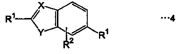
ここで、上記化学式2〜36中のR1は下記化学式37に示すような2価の構造を示し、別の骨格と連結する連結基を示す。これらの液晶性分子にR1が複数個ある場合には、それぞれが同一でもよいし、異なっていてもよい。また、これらの液晶性分子にR1はなくてもよい。上記化学式2〜36中のR2は下記化学式38に示すような官能基を示す。これらの液晶性分子にR2が複数個ある場合には、それぞれが同一でもよいし、異なっていてもよい。また、上記化学式2〜36中のXはCH又はNを示し、上記化学式2〜36中のYはS又はOを示す。Here, R 1 in the chemical formulas 2 to 36 represents a divalent structure as shown in the following chemical formula 37, and represents a linking group linked to another skeleton. When there are a plurality of R 1 in these liquid crystalline molecules, each may be the same or different. Further, R 1 may not be present in these liquid crystalline molecules. R 2 in the chemical formulas 2 to 36 represents a functional group as shown in the following chemical formula 38. When there are a plurality of R 2 in these liquid crystalline molecules, each may be the same or different. X in the chemical formulas 2 to 36 represents CH or N, and Y in the chemical formulas 2 to 36 represents S or O.
上記化学式1のB及びB’は、屈曲性の高い鎖状構造、又は、水素若しくはハロゲン等の官能基である。屈曲性の高い鎖状構造は、基本的には直鎖状アルキル鎖又は分岐鎖状アルキル鎖であるが、このようなアルキル鎖には下記化学式37に示す39個の2価の構造の群から選択される構造が含まれていてもよい。また、屈曲性の高い鎖状構造は、下記化学式37に示す39個の2価の構造の群から選択された構造のみで構成されてもよく、この場合にはこの群から選択された1つの構造で構成されてもよいし、この群から選択された複数の構造が直鎖状又は分岐状に連結して構成されていてもよい。また、これらの屈曲性の高い鎖状構造は、置換基として下記化学式38に例示した21個の官能基の群から選択された官能基を有していてもよい。なお、上記化学式1中のB及びB’は、屈曲性の高い鎖状構造をとらない場合に、下記化学式38に例示した21個の官能基のいずれかとなる。 B and B ′ in the chemical formula 1 are highly flexible chain structures or functional groups such as hydrogen or halogen. A highly flexible chain structure is basically a linear alkyl chain or a branched alkyl chain, and such an alkyl chain includes a group of 39 divalent structures represented by the following chemical formula 37. The structure to be selected may be included. In addition, the highly flexible chain structure may be constituted only by a structure selected from a group of 39 divalent structures represented by the following chemical formula 37. In this case, one chain selected from this group is selected. The structure may be comprised, and the some structure selected from this group may be comprised by connecting with linear form or branched form. Further, these highly flexible chain structures may have a functional group selected from the group of 21 functional groups exemplified in Chemical Formula 38 below as a substituent. In addition, B and B ′ in the chemical formula 1 are any of the 21 functional groups exemplified in the following chemical formula 38 when not having a highly flexible chain structure.
但し、上記化学式38中のRは、炭素数1〜40の直鎖アルキル基又は分岐アルキル基を表す。 However, R in the said Chemical formula 38 represents a C1-C40 linear alkyl group or a branched alkyl group.
本発明に適用される液晶性有機半導体材料には、上記化学式1に示した液晶性分子のうち、熱分解温度以下の温度において、少なくとも一種類の液晶状態を持つものが用いられる。「熱分解温度以下の温度において」とは、その材料がそれ自身分解されない状態を意味するものである。熱分解温度は、適用される材料により異なる。また、「少なくとも一種類の液晶状態を持つもの」とは、最低一種類の液晶状態を持つものが使用されるという意味である。例えば、後述するスメクティック液晶相(以下、Smともいう)においては、SmA相、SmB相、SmC相等の複数種類の液晶状態を有し、そのうちの少なくとも一種類の液晶状態を持つことである。 As the liquid crystalline organic semiconductor material applied to the present invention, those having at least one liquid crystal state at a temperature equal to or lower than the thermal decomposition temperature among the liquid crystalline molecules represented by the above chemical formula 1 are used. “At a temperature below the thermal decomposition temperature” means a state in which the material does not decompose itself. The pyrolysis temperature depends on the applied material. The phrase “having at least one kind of liquid crystal state” means that one having at least one kind of liquid crystal state is used. For example, a smectic liquid crystal phase (hereinafter also referred to as Sm) described later has a plurality of types of liquid crystal states such as an SmA phase, an SmB phase, and an SmC phase, and has at least one type of liquid crystal state.
液晶性有機半導体材料は、少なくとも一種類のサーモトロピック液晶状態を持つ有機半導体材料、及び、少なくとも一種類のリオトロピック液晶状態を持つ有機半導体材料に分けることができる。なお、サーモトロピック液晶(Thermotropic LC)とは、ある温度範囲機で液晶になる物質であり、本発明においては、分子配列の違いにより、スメクティック液晶及びネマティック液晶が含まれる。また、リオトロピック液晶(ライオトロピック液晶ともいう。Liotropic LC)とは、溶媒の存在下で液晶となるものであり、特に温度によらずに濃度変化だけで起こることがあり、濃度転移方液晶と呼ばれることもある。 The liquid crystalline organic semiconductor material can be divided into an organic semiconductor material having at least one kind of thermotropic liquid crystal state and an organic semiconductor material having at least one kind of lyotropic liquid crystal state. The thermotropic liquid crystal (Thermotropic LC) is a substance that becomes a liquid crystal in a certain temperature range machine, and in the present invention, a smectic liquid crystal and a nematic liquid crystal are included due to a difference in molecular arrangement. In addition, lyotropic liquid crystal (also referred to as lyotropic liquid crystal: Liotropic LC) is a liquid crystal in the presence of a solvent, and may occur only by a concentration change regardless of temperature, and is called a concentration transition liquid crystal. Sometimes.
液晶性有機半導体材料は、上述の材料のうち、ロッド状のスメクティック液晶状態を持つ材料であることが好ましい。液晶は自己組織化機能を有するので自発的に分子秩序が形成され、特にこのようなスメクティック液晶相状態を持つ液晶性有機半導体材料を用いて形成された有機半導体層14は、分子結晶の様な優れた電荷輸送特性を示すことができる。有機半導体層14は、そのような観点から、高次のスメクティック相状態を持つ液晶性有機半導体材料で形成されていることが好ましい。 The liquid crystalline organic semiconductor material is preferably a material having a rod-like smectic liquid crystal state among the above-described materials. Since the liquid crystal has a self-organizing function, a molecular order is spontaneously formed. In particular, the
このような液晶性有機半導体材料により形成された有機半導体層14は、ホッピング伝導に基づいた高い電子と正孔についていずれも高速の電荷輸送能が発現する、という電荷移動特性に関する顕著な効果を有している。すなわち、有機半導体層14を構成する液晶性分子は、骨格構造の片末端又は両末端に導入されているアルキル鎖等の鎖状分子の存在により自己組織化を起こし、極めて秩序的に配向するので、有機半導体層14には液晶性分子により高い自己組織性を有した分子凝集部分である領域が形成される。その領域においては、液晶性分子のπ電子芳香環を有する骨格構造部位が、隣接する分子間と極めて小さな距離で隣接する。その結果、液晶性分子の領域では、π電子軌道の重なりが大きくなることにより、ホッピング伝導に基づいた高速の電子伝導と高速のホール伝導が起こるので、形成された有機半導体層は、高い電荷輸送特性を示すこととなる。なお、この場合における骨格構造同士の間隔は0.3〜0.5nm程度である。形成された有機半導体層は、液晶性分子の自己組織化により剛直なπ電子芳香環がかなりの長距離にわたり連続して重なり合う領域を有するので、電子やホールのホッピング伝導を容易に起こすことになる。これに対し、微結晶のように高い分子秩序が長距離にわたって実現していない有機半導体の場合には、結晶粒界でトラップが生成し、高い伝導性は期待できない。 The
一方で、スメクティック液晶相を呈する有機半導体層14は、鎖状構造がリッチとなる領域を持っている。この領域は、上述した領域(液晶性分子により高い自己組織性を有した分子凝集部分である領域)の電荷の輸送経路となる層を隔てる緩衝層として機能し、大きな電荷輸送異方性を発現させる効果を有する。 On the other hand, the
スメクティック液晶相状態を持つ液晶性分子の具体例としては、フェニルナフタレン骨格を有する下記の化学式39の2−(4’−octylphenyl)−6−dodecyloxynaphthalene(8−PNP−O12と略す)及び化学式40の2−(4’−octylphenyl)−6−butyloxynaphthalene(8−PNP−O4と略す)、ターチオフェン骨格を有する下記の化学式41のdidodecylterthiophene及び化学式42のdihexylterthiophene、フェニルベンゾチアゾール骨格を有する下記の化学式43の2−(4’−heptyloxyphenyl)−6−dodecylthiobenzothiazoleで表される液晶性分子を例示することができる。これらの液晶性分子からなる液晶性有機半導体材料は、同一相内で、電子輸送性及び正孔輸送性のどちらも有し(すなわち輸送の両極性を有し)、いずれの輸送性も、ホッピング伝導による電荷移動度が電界強度及び温度に依存しない。 Specific examples of the liquid crystalline molecule having a smectic liquid crystal phase state include 2- (4′-octylphenyl) -6-dodecyloxynaphthalene (abbreviated as 8-PNP-O12) of the following chemical formula 39 having a phenylnaphthalene skeleton and a chemical formula of 40 2- (4′-octylphenyl) -6-butyloxynaphthalene (abbreviated as 8-PNP-O4), a didecylterthiophene of the following chemical formula 41 having a terthiophene skeleton, and a dihexylterthiophene of the chemical formula 42 having the following chemical formula 43 Illustrative of a liquid crystalline molecule represented by 2- (4′-heptyloxyphenyl) -6-dodecylthiobenzothiozole Door can be. The liquid crystalline organic semiconductor material composed of these liquid crystalline molecules has both electron transport properties and hole transport properties within the same phase (ie, has both transport polarities), and both transport properties are hopping. The charge mobility due to conduction is independent of the electric field strength and temperature.
少なくとも一種類のサーモトロピック液晶状態を持つ有機半導体材料(以下、有機半導体材料Iということもある。)からなる有機半導体層は、この有機半導体材料Iをサーモトロピック液晶相を維持又は経由できる温度に保持した後にその温度から冷却することにより形成される。このときの冷却を速やかに行った場合(すなわち急冷した場合)には、高次の構造(高い構造性)を有する相(好ましくはスメクティック相)がガラス状態に固定された有機半導体層を得ることができる。このようにして形成された有機半導体層は、高い電荷移動特性を有している。また、このときの冷却を緩やかに行った場合(すなわち徐冷した場合)には、少なくとも一部が結晶状態となった高い秩序性を有する有機半導体層を得ることができる。このようにして得られた有機半導体層は、有機半導体材料の結晶サイズが大きくなり、高い電荷移動度を発現する。特に、その結晶サイズが電荷移動に関与する電極間距離よりも大きい場合に、より高い電荷移動度が得られる。なお、本明細書において「結晶相」又は「結晶状態」とは、液晶性有機半導体材料が液晶−結晶相転移温度以下の凝集状態になっていることをいう。 The organic semiconductor layer made of an organic semiconductor material having at least one kind of thermotropic liquid crystal state (hereinafter, also referred to as organic semiconductor material I) has a temperature at which the organic semiconductor material I can be maintained or passed through the thermotropic liquid crystal phase. It is formed by holding and cooling from that temperature. When the cooling at this time is promptly performed (that is, when rapidly cooled), an organic semiconductor layer in which a phase having a higher-order structure (high structure) (preferably a smectic phase) is fixed in a glass state is obtained. Can do. The organic semiconductor layer thus formed has high charge transfer characteristics. In addition, when the cooling at this time is performed slowly (that is, when the cooling is performed slowly), an organic semiconductor layer having high ordering in which at least a part is in a crystalline state can be obtained. The organic semiconductor layer thus obtained has a large crystal size of the organic semiconductor material and exhibits high charge mobility. In particular, higher charge mobility can be obtained when the crystal size is larger than the interelectrode distance involved in charge transfer. In the present specification, the “crystalline phase” or “crystalline state” means that the liquid crystalline organic semiconductor material is in an aggregated state of a liquid crystal-crystalline phase transition temperature or lower.
また、少なくとも一種類のリオトロピック液晶状態を持つ有機半導体材料(以下、有機半導体材料Iということもある。)からなる有機半導体層は、その有機半導体材料IIをリオトロピック液晶相を呈する濃度に保持した後に溶媒を徐々に除くことにより形成される。このようにして形成された有機半導体層は、良好な配向状態を有しており広い範囲で高い配向性が実現され、また、高い電荷移動度を発現する。 In addition, the organic semiconductor layer made of an organic semiconductor material having at least one kind of lyotropic liquid crystal state (hereinafter, also referred to as organic semiconductor material I) has the organic semiconductor material II held at a concentration exhibiting a lyotropic liquid crystal phase. It is formed by gradually removing the solvent. The organic semiconductor layer thus formed has a good alignment state, realizes a high degree of orientation in a wide range, and exhibits high charge mobility.
有機半導体材料Iは、液晶状態を維持する温度において流動性を有するので、その状態で塗布することができる。また、有機半導体材料IIは、溶媒を除去する前において流動性を有するので、その状態で塗布することができる。こうした方法によれば、電荷移動度が均一で大面積の有機半導体層を極めて容易に形成することができる。このときの塗布方法としては、スピンコート法又はダイコート法等の塗布方法のほか、インクジェット法等の印刷方法を用いることができる。なお、有機半導体材料Iを用いて有機半導体層を形成する場合には、有機半導体材料Iを溶媒で希釈した溶液を塗布することもできる。このような場合に、溶媒の乾燥状況により塗膜に多様なモホロジが生ずることがあるが、塗布後に液晶性を利用した熱アニール処理を施すことにより、有機半導体層の膜質の均一化を図ることができる。有機半導体層14の層厚は、0.05〜1.0μm程度である。 Since the organic semiconductor material I has fluidity at a temperature at which the liquid crystal state is maintained, it can be applied in that state. Moreover, since the organic semiconductor material II has fluidity before removing the solvent, it can be applied in that state. According to such a method, an organic semiconductor layer having a uniform charge mobility and a large area can be formed very easily. As a coating method at this time, in addition to a coating method such as a spin coating method or a die coating method, a printing method such as an ink jet method can be used. In addition, when forming an organic-semiconductor layer using the organic-semiconductor material I, the solution which diluted the organic-semiconductor material I with the solvent can also be apply | coated. In such a case, various morphology may occur in the coating film depending on the drying condition of the solvent, but the film quality of the organic semiconductor layer should be made uniform by performing a thermal annealing process utilizing liquid crystallinity after coating. Can do. The layer thickness of the
本発明の有機半導体装置10において、有機半導体層14は、10−6cm2/V・s以上の電荷移動度を示すことが好ましい。In the
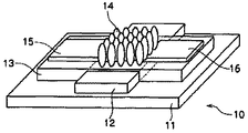
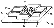
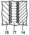
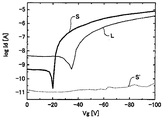
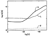
なお、液晶性分子は一定の向きに配向し易いので、有機半導体層において液晶性分子を分子結晶のように規則正しく配列させることができ、液晶性分子のスメクティック相由来の分子層内における分子間距離の平均値を0.3〜0.4nmと極めて小さくすることもできる。液晶性分子の配向態様としては、(イ)図2に示すように、ゲート絶縁層13の上に形成されたドレイン電極16とソース電極15の膜厚方向に平行に配向している態様、又は、(ロ)図3に示すように、ゲート絶縁層13の上に形成されたドレイン電極16とソース電極15の膜厚方向に直交し、かつ、当該ドレイン電極16とソース電極15の間に横列するように配向している態様、等を挙げることができる。また、液晶性分子の配向手段としては、有機半導体層14が形成される基材(例えば、ゲート絶縁層13の表面等。)に、液晶配向層を形成したり、ラビング処理等の配向処理をしたり、あるいは、配向処理を施した層と接触させたりする手段を挙げることができる。こうした分子間距離で結晶状態を形成した有機半導体層は、分子相互の電子相関が極めて大きくなり、キャリアのホッピング確率が大きく、高い電荷輸送特性を示すという効果がある。例えば、上述の化学式25のスメクティック液晶性を有する液晶性分子の分子間距離の平均値が0.3〜0.4nmの場合においては、電荷移動度が10−3〜10−2cm2/V・sという高い電荷輸送特性を有する。Since liquid crystalline molecules are easily oriented in a certain direction, the liquid crystalline molecules can be regularly arranged like molecular crystals in the organic semiconductor layer, and the intermolecular distance in the molecular layer derived from the smectic phase of the liquid crystalline molecules. The average value can be made extremely small, 0.3 to 0.4 nm. As the orientation mode of the liquid crystal molecules, (a) as shown in FIG. 2, the mode in which the
(電荷注入促進層)
電荷注入促進層17、18は、有機半導体層14とソース電極15及びドレイン電極16うち少なくとも一方の電極との間に設けられるものであり、電極15,16の仕事関数と有機半導体層14の仕事関数との差を小さくするように作用する。すなわち、有機半導体層14とソース電極15及びドレイン電極16のうち少なくとも一方の電極との間に存在する電荷注入障壁を小さくするように作用する。このような作用により、電極から有機半導体層への電荷の注入が容易に促進される。(Charge injection promoting layer)
The charge
電荷注入促進層は、通常、電荷を注入するソース電極15側に設けられている。有機半導体層14が正孔の輸送経路として作用する場合には、ソース電極15側に形成された電荷注入促進層17を、ソース電極15から有機半導体層14に正孔を注入し易くさせる層として機能させることができる。また、有機半導体層14が電子の輸送経路として作用する場合には、ソース電極15側に形成された電荷注入促進層17を、ソース電極15から有機半導体層14に電子を注入し易くさせる層として機能させることができる。 The charge injection promoting layer is usually provided on the
また、電荷注入促進層は、ドレイン電極16側にも設けられていることが好ましい。ドレイン電極16側に設けられた電荷注入促進層18がソース電極15側に設けられた電荷注入促進層17と同種のものである場合(すなわち電荷注入促進層17及び18の双方が正孔の注入を促進させる層である場合や電荷注入促進層17及び18の双方が電子の注入を促進させる層である場合)には、ソース電極15とドレイン電極16の機能を入れ替えることができることにより、有機半導体装置10を、その装置に接続する負荷への電荷の書き込み及び引き抜きに利用することができる。一方、ドレイン電極16側に設けられた電荷注入促進層18がソース電極15側に設けられた電荷注入促進層17と異種のものである場合(すなわち電荷注入促進層17及び18の一方が正孔の注入を促進させる層であり他方が電子の注入を促進させる層である場合)には、有機半導体装置10をより低電流で駆動させることができる。 The charge injection promoting layer is preferably provided also on the
本発明に適用される電荷注入促進層は、双極子モーメントを有する有機薄膜である。このような有機薄膜は電気双極子モーメントを有する有機化合物で形成される。 The charge injection promoting layer applied to the present invention is an organic thin film having a dipole moment. Such an organic thin film is formed of an organic compound having an electric dipole moment.
まず、正孔の注入を促進させる層として電荷注入促進層を機能させる場合について説明する。以下、正孔の注入を促進させる電荷注入促進層を「正孔注入促進層」ということもある。 First, the case where the charge injection promoting layer is made to function as a layer that promotes hole injection will be described. Hereinafter, the charge injection promoting layer that promotes the injection of holes may be referred to as a “hole injection promoting layer”.
正孔注入促進層は、1デバイ以上50デバイ以下の間に絶対値を持つベクトルで表される電気双極子モーメントを有した有機化合物で形成され、そのベクトルの向きは、有機化合物の正極が正バイアスされる電極側に位置し、その有機化合物の負極が有機半導体層側に位置することになる向きである。ここで、正バイアスされる電極は、正孔を注入する電極であり、通常ソース電極15である。また、負バイアスされる電極は、注入された正孔を取り込む電極であり、通常ドレイン電極16である。このような電気双極子モーメントを持つ有機化合物が正バイアスされる電極に化学的に結合することにより電気二重層が形成されるので、正バイアスされた電極から有機半導体層14に正孔を容易に注入できる。 The hole injection promoting layer is formed of an organic compound having an electric dipole moment represented by a vector having an absolute value between 1 Debye and 50 Debye, and the direction of the vector is such that the positive electrode of the organic compound is positive. It is positioned on the side of the electrode to be biased, and the organic compound negative electrode is positioned on the organic semiconductor layer side. Here, the positively biased electrode is an electrode for injecting holes, and is usually the
具体的には、上述した有機半導体層14のHOMOレベルに合わせて、正孔注入促進層形成用材料(1デバイ〜50デバイの間に絶対値を持つベクトルで表される電気双極子モーメントを有した有機化合物)が選択される。例えば、上記化学式40の液晶性分子(8−PNP−O4)からなる液晶性有機半導体材料で形成された有機半導体層14のHOMOの値は6.0eVであり、ITOで形成されたソース電極15の仕事関数は4.7eVである。そのため、有機半導体層とソース電極15のエネルギーギャップである約1.7eVの注入障壁を小さくする材料が選択される。 Specifically, in accordance with the HOMO level of the
本発明では例えばソース電極15の有機半導体層側の界面に、下記化学式44で表される有機化合物が集合してなる双極子モーメントを有する有機薄膜が形成される。ここで、Yは電極又は電極近傍の反応性基との連結基であり、Xは置換基であり、Arは、芳香族炭化水素環又は芳香族複素環である。 In the present invention, for example, an organic thin film having a dipole moment formed by aggregation of organic compounds represented by the following chemical formula 44 is formed at the interface of the
![]()
![]()
式44において、連結基Yは例えばソース電極15の表面と結合し、これが集合することにより双極子モーメントを有する有機薄膜が形成される。ここで、「双極子モーメントを有する有機薄膜」とは、厚さが分子1個の大きさに相当する薄膜を意味する。なお、式44で表される構造が一部共有結合して2量体、3量体又はオリゴマー状の構造を形成していてもよいが、その層の厚さは分子1個分である。 In Formula 44, the linking group Y is bonded to, for example, the surface of the
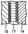
連結基Yは、通常、ソース電極15の表面に存在する反応性官能基(多くの場合は水酸基)と反応して連結する。図4は、芳香族炭化水素環又は芳香族複素環からなるArの両側に連結基Yと置換基Xが配位することにより付与される双極子モーメントを有する有機薄膜(正孔注入促進層)17がソース電極15の表面に形成された模式図である。この正孔注入促進層17が備える電気二重層による電場により、ソース電極15の仕事関数を増加させることができる。 The linking group Y usually reacts with and reacts with a reactive functional group (in many cases, a hydroxyl group) present on the surface of the
連結基Yは、少なくとも酸素原子とハロゲン原子を含有する基であるが、好ましくは、下記化学式45に示す5個の基から選ばれる。 The linking group Y is a group containing at least an oxygen atom and a halogen atom, and is preferably selected from five groups represented by the following chemical formula 45.
この式45中、Z1及びZ2は、各々独立にハロゲン原子を表し、特に塩素原子が好ましい。 In Formula 45, Z1 and Z2 each independently represent a halogen atom, and a chlorine atom is particularly preferable.
Arは、置換基Xを有する2価の芳香族炭化水素環又は芳香族複素環を表し、5〜6員環の単環、又は2〜3個縮合もしくは直接結合してなる2価の基であることが好ましい。特に、ベンゼン、ナフタレン、ビフェニル、アントラセン、チオフェン、フラン、ピリジン等であることが好ましい。 Ar represents a divalent aromatic hydrocarbon ring or aromatic heterocycle having a substituent X, and is a 5- to 6-membered monocyclic ring or a divalent group formed by condensing or directly bonding 2 to 3 rings. Preferably there is. In particular, benzene, naphthalene, biphenyl, anthracene, thiophene, furan, pyridine and the like are preferable.
置換基Xは、好ましくは、水素原子、塩素原子等のハロゲン原子;ニトロ基;メチル基、エチル基等の炭素数1〜6のアルキル基;ベンジル基等のアラルキル基;ビニル基等のアルケニル基;シアノ基;アセチレン等のアルキニル基;アミド基;アセチル基等のアシル基;メトキシカルボニル基、エトキシカルボニル基等の炭素数1〜6のアルコキシカルボニル基;カルボキシル基;メトキシ基、エトキシ基等の炭素数1〜6のアルコキシ基;フェノキシ基、ベンジルオキシ基などのアリールオキシ基;トリフルオロメチル基等のハロアルキル基;チオシアノ基;メタンスルフォニル基等のアルキルスルフォニル基;スルフォンアミド基を好ましく挙げることができる。特に好ましくは、ハロゲン原子、ハロアルキル基、シアノ基、ニトロ基から選ばれる。 The substituent X is preferably a halogen atom such as a hydrogen atom or a chlorine atom; a nitro group; an alkyl group having 1 to 6 carbon atoms such as a methyl group or an ethyl group; an aralkyl group such as a benzyl group; an alkenyl group such as a vinyl group. Cyano group; alkynyl group such as acetylene; amide group; acyl group such as acetyl group; alkoxycarbonyl group having 1 to 6 carbon atoms such as methoxycarbonyl group and ethoxycarbonyl group; carboxyl group; carbon such as methoxy group and ethoxy group; Preferred examples include an alkoxy group of 1 to 6; an aryloxy group such as a phenoxy group and a benzyloxy group; a haloalkyl group such as a trifluoromethyl group; a thiocyano group; an alkylsulfonyl group such as a methanesulfonyl group; and a sulfonamide group. . Particularly preferably, it is selected from a halogen atom, a haloalkyl group, a cyano group, and a nitro group.
置換基Xとしては、上述した基の中でも特に電子吸引性基が好ましく選択される。ここで電子吸引性基とは、ハメット定数(σm、σp)が正の値を有する置換基である。本発明では、Arの部分がπ共役系である化合物41を採用しているために、この部分が非共役系の直鎖アルキル化合物におけるような絶縁体形成はなく、電気二重層の効果を十分に引き出すことができる。 As the substituent X, an electron-withdrawing group is particularly preferably selected from the groups described above. Here, the electron-withdrawing group is a substituent having a positive Hammett constant (σm, σp). In the present invention, since the Ar portion is a compound 41 having a π-conjugated system, there is no insulator formation as in a non-conjugated linear alkyl compound, and the effect of the electric double layer is sufficiently obtained. Can be pulled out.
次に、電子の注入を促進させる層として電荷注入促進層を機能させる場合について説明する。以下、電子の注入を促進させる層である電荷注入促進層を「電子注入促進層」ということもある。 Next, a case where the charge injection promoting layer is made to function as a layer that promotes electron injection will be described. Hereinafter, the charge injection promoting layer, which is a layer that promotes electron injection, may be referred to as an “electron injection promoting layer”.
電子注入促進層は、1デバイ以上50デバイ以下の間に絶対値を持つベクトルで表される電気双極子モーメントを有した有機化合物で形成され、そのベクトルの向きは、有機化合物の負極が負バイアスされた電極側に位置し、その有機化合物の正極が有機半導体層側に位置することになる向きである。ここで、負バイアスされた電極は、電子を注入する電極であり、通常ソース電極15である。また、正バイアスされた電極は、注入された電子を取り込む電極であり、通常ドレイン電極16である。このような電気双極子モーメントを持つ有機化合物が負バイアスされる電極に化学的に結合することにより電気二重層が形成されるので、負バイアスされた電極から有機半導体層14に電子を容易に注入できる。 The electron injection promoting layer is formed of an organic compound having an electric dipole moment represented by a vector having an absolute value between 1 Debye and 50 Debye, and the direction of the vector is such that the negative electrode of the organic compound is negatively biased. The positive electrode of the organic compound is located on the organic semiconductor layer side. Here, the negatively biased electrode is an electrode for injecting electrons, and is usually the
具体的には、上述した有機半導体層14のLUMOレベルに合わせて、その双極子モーメントを有する電子注入促進層形成用材料(1デバイ〜50デバイの間に絶対値を持つベクトルで表される電気双極子モーメントを有した有機化合物)が選択される。例えば、上記化学式40の液晶性分子(8−PNP−O4)からなる液晶性有機半導体材料で形成された有機半導体層14のLUMOの値は1.6eVであり、ITOで形成されたソース電極15の仕事関数は5.0eVである。そのため、有機半導体層とソース電極15のエネルギーギャップである約3.4eVの注入障壁を小さくする注入材料が選択される。 Specifically, in accordance with the LUMO level of the
本発明では、例えばソース電極15の有機半導体層側の界面に、下記化学式46で表される有機化合物が集合してなる電子注入促進層17が形成される。 In the present invention, for example, the electron
![]()
![]()
式46において、連結基Y’は電極の表面と結合し、これが集合することにより双極子モーメントを有する有機薄膜が形成される。この場合の「単分子膜」も上記同様、厚さが分子1個の大きさに相当する薄膜を意味する。なお、式43で表される構造が一部共有結合して2量体、3量体又はオリゴマー状の構造を形成していてもよいが、その層の厚さは分子1個分である。 In Formula 46, the linking group Y ′ is bonded to the surface of the electrode, and the organic thin film having a dipole moment is formed by aggregation. The “monomolecular film” in this case also means a thin film having a thickness corresponding to the size of one molecule, as described above. Note that a part of the structure represented by Formula 43 may be covalently bonded to form a dimer, trimer, or oligomer structure, but the thickness of the layer is one molecule.
連結基Y’は、通常、ソース電極の表面に存在する反応性官能基(多くの場合は水酸基)と反応して連結する。図5は、芳香族炭化水素環又は芳香族複素環からなるArの両側に連結基Y’と置換基X’が配位することにより付与される双極子モーメントを有する有機薄膜(電子注入促進層)17がソース電極15の表面に形成された模式図である。この電子注入促進層17が備える電気二重層による電場により、ソース電極15の仕事関数を減少させることができる。 The linking group Y ′ usually reacts and links with a reactive functional group (in many cases, a hydroxyl group) present on the surface of the source electrode. FIG. 5 shows an organic thin film (electron injection promoting layer) having a dipole moment imparted by coordination of a linking group Y ′ and a substituent X ′ on both sides of Ar composed of an aromatic hydrocarbon ring or an aromatic heterocycle. ) 17 is a schematic view formed on the surface of the
連結基Y’は、少なくとも酸素原子とハロゲン原子を含有する基であるが、好ましくは、上記同様に化学式45に示す基から選ばれる。 The linking group Y ′ is a group containing at least an oxygen atom and a halogen atom, and is preferably selected from the groups represented by Chemical Formula 45 as described above.
Arは、置換基Xを有する2価の芳香族炭化水素環又は芳香族複素環を表し、5〜6員環の単環、又は2〜3個縮合もしくは直接結合してなる2価の基であることが好ましい。特に、ベンゼン、ナフタレン、ビフェニル、アントラセン、チオフェン、フラン、ピリジン等であることが好ましい。 Ar represents a divalent aromatic hydrocarbon ring or aromatic heterocycle having a substituent X, and is a 5- to 6-membered monocyclic ring or a divalent group formed by condensing or directly bonding 2 to 3 rings. Preferably there is. In particular, benzene, naphthalene, biphenyl, anthracene, thiophene, furan, pyridine and the like are preferable.
置換基X’は、好ましくは、水素原子、塩素原子等のハロゲン原子;ニトロ基;メチル基、エチル基等の炭素数1〜6のアルキル基;ベンジル基等のアラルキル基;ビニル基等のアルケニル基;シアノ基;アセチレン等のアルキニル基;アミド基;アセチル基等のアシル基;メトキシカルボニル基、エトキシカルボニル基等の炭素数1〜6のアルコキシカルボニル基;カルボキシル基;メトキシ基、エトキシ基等の炭素数1〜6のアルコキシ基;フェノキシ基、ベンジルオキシ基などのアリールオキシ基;トリフルオロメチル基等のハロアルキル基;チオシアノ基;メタンスルフォニル基等のアルキルスルフォニル基;スルフォンアミド基を好ましく挙げることができる。特に好ましくは、ハロゲン原子、ハロアルキル基、シアノ基、ニトロ基から選ばれる。 The substituent X ′ is preferably a halogen atom such as a hydrogen atom or a chlorine atom; a nitro group; an alkyl group having 1 to 6 carbon atoms such as a methyl group or an ethyl group; an aralkyl group such as a benzyl group; an alkenyl such as a vinyl group. Group; cyano group; alkynyl group such as acetylene; amide group; acyl group such as acetyl group; alkoxycarbonyl group having 1 to 6 carbon atoms such as methoxycarbonyl group and ethoxycarbonyl group; carboxyl group; methoxy group, ethoxy group and the like Preferred examples include an alkoxy group having 1 to 6 carbon atoms; an aryloxy group such as a phenoxy group and a benzyloxy group; a haloalkyl group such as a trifluoromethyl group; a thiocyano group; an alkylsulfonyl group such as a methanesulfonyl group; and a sulfonamide group. it can. Particularly preferably, it is selected from a halogen atom, a haloalkyl group, a cyano group, and a nitro group.
置換基X’としては、上述した基の中でも特に電子供与性基が好ましく選択される。ここで電子供与性基とは、ハメット定数(σm、σp)が負の値を有する置換基である。本発明では、Arの部分がπ共役系である化合物43を採用しているために、この部分が非共役系の直鎖アルキル化合物におけるような絶縁体形成はなく、電気二重層の効果を十分に引き出すことができる。 As the substituent X ′, an electron donating group is particularly preferably selected from the groups described above. Here, the electron donating group is a substituent having a negative Hammett constant (σm, σp). In the present invention, since the Ar portion is a compound 43 having a π-conjugated system, there is no insulator formation as in the case of a non-conjugated linear alkyl compound, and the effect of the electric double layer is sufficient. Can be pulled out.
電荷注入促進層17,18は、電極と有機半導体層の間に設けられており、具体的にはソース電極15及びドレイン電極16の少なくとも一方の電極上、又は、ソース電極15及びドレイン電極16の少なくとも一方の電極の近傍のチャネル領域内に設けられている。ここで「電極の近傍のチャネル領域内」とは、電極の端部等少なくとも一部と接していることで有機半導体層への電荷の注入を促進することができる領域内を意味する。 The charge
電荷注入促進層17,18は、例えば有機半導体層形成前にソース電極15及びドレイン電極16上に、電荷注入促進層形成用溶液を塗布又は蒸着することにより形成される。この場合に、有機半導体層14は通常、電荷注入促進層17、18が形成された後に形成される。その双極子モーメントを有する電荷注入促進層形成用溶液の組成は、0.01〜100ミリモル/リットルの割合で構成される。 The charge
(層間絶縁層)
有機半導体装置10には、層間絶縁層を設けることが望ましい。層間絶縁層は、ゲート絶縁層13上にソース電極15及びドレイン電極16を形成する際に、ゲート電極12の表面の汚染を防ぐことを目的として形成される。したがって、層間絶縁層は、ソース電極15及びドレイン電極16を形成する前にゲート絶縁層13の上に形成される。そして、ソース電極15及びドレイン電極16が形成された後においては、チャネル領域上方に位置する部分を完全に除去又は一部を除去するように加工される。除去される層間絶縁層領域は、ゲート電極12のサイズと同等であることが望ましい。(Interlayer insulation layer)
The
層間絶縁層を構成する材料としては、ケイ素酸化物、ケイ素窒化物、酸化アルミニウム等の無機材料や、ポリクロロピレン、ポリエチレンテレフタレート、ポリオキシメチレン、ポリビニルクロライド、ポリフッ化ビニリデン、シアノエチルプルラン、ポリメチルメタクリレート、ポリスルホン、ポリカーボネート、ポリイミド等の有機材料が挙げられる。 As the material constituting the interlayer insulating layer, inorganic materials such as silicon oxide, silicon nitride, aluminum oxide, polychloropyrene, polyethylene terephthalate, polyoxymethylene, polyvinyl chloride, polyvinylidene fluoride, cyanoethyl pullulan, polymethyl methacrylate, Examples thereof include organic materials such as polysulfone, polycarbonate, and polyimide.
(有機半導体装置)
上記のような構成を有する本発明の有機半導体装置10においては、ソース電極15及びドレイン電極16のうち少なくとも一方の電極と有機半導体層14との間に電荷注入促進層17,18が形成されているので、有機半導体層14に容易に電荷が注入される。特に、有機半導体層14が液晶性有機半導体材料により形成された場合には、この層に充分な量の電荷が供給されるので、多くの電荷が高速で移動する有機半導体装置10となる。さらに、有機半導体装置10では、有機半導体層14とソース電極15及びドレイン電極16との間のオーミックコンタクトの改善が求められているが、本発明の有機半導体装置では、電極の仕事関数と有機半導体層の仕事関数との差を小さくすることができるので、良好なオーミックコンタクトの形成を実現することができ、その結果、有機半導体装置が動作するしきい電圧を低減させることができる。(Organic semiconductor device)
In the
なお、上記では図1に示すコプラナー構造の有機トランジスタ素子を例にして説明したが、本発明は他の構造を有する有機トランジスタ素子にも適用できる。
他の構造を有する有機トランジスタとしては、例えば、図6や図7に示す有機トランジスタ素子が挙げられる。In the above description, the organic transistor element having the coplanar structure shown in FIG. 1 has been described as an example. However, the present invention can also be applied to organic transistor elements having other structures.
As an organic transistor which has another structure, the organic transistor element shown in FIG. 6 and FIG. 7 is mentioned, for example.
図6に示す有機トランジスタ素子は、第1の基板11と、ゲート電極12と、ゲート絶縁層13と、有機半導体層14と、電荷注入促進層17及び18と、ソース電極15及びドレイン電極16と、第2の電極基板11’とがこの順で積層されているスタガ型の構造を有する。また、図7に示す有機トランジスタ素子は、第1の基板11と、ゲート電極12と、ゲート絶縁層13と、ソース電極15と、電荷注入促進層17と、有機半導体層14と、電荷注入促進層18と、ドレイン電極16と、第2の電極基板11’とがこの順で積層されている構造を有し、有機半導体層の層厚方向の電荷輸送を利用するものである。 The organic transistor element shown in FIG. 6 includes a
また、本発明は有機トランジスタ素子のような3極の有機半導体装置だけではなく、有機ダイオード素子のような2極の有機半導体装置にも適用できる。 The present invention can be applied not only to a tripolar organic semiconductor device such as an organic transistor element but also to a bipolar organic semiconductor device such as an organic diode element.
次に、本発明を実施例によって更に具体的に説明する。本発明はその要旨を超えない限り、以下の実施例の記載に限定されるものではない。 Next, the present invention will be described more specifically with reference to examples. The present invention is not limited to the description of the following examples unless it exceeds the gist.
(実施例1)
実施例1の有機半導体装置として、スタガ型の有機トランジスタ素子を作成した。(Example 1)
As the organic semiconductor device of Example 1, a staggered organic transistor element was prepared.
無アルカリガラス基板(コーニング社製、製品番号:1737)上に、スパッタ法によりシート抵抗10ΩcmのITO薄膜を形成し、フォトリソグラフィ法にてチャネル長50μm、チャネル幅1mmのソース・ドレイン電極対を形成した。ソース・ドレイン電極対が形成されたガラス基板には、所望でない導電経路由来のリーク電流を抑制するために、有機トランジスタ素子の形成領域のみが露出するように、フォトリソグラフィ法及びリフトオフ法によりSiO2スパッタ膜からなるパッシベーション膜を設けた。An ITO thin film having a sheet resistance of 10 Ωcm is formed by sputtering on an alkali-free glass substrate (Corning, product number: 1737), and a source / drain electrode pair having a channel length of 50 μm and a channel width of 1 mm is formed by photolithography. did. In order to suppress a leakage current derived from an undesired conductive path, the glass substrate on which the source / drain electrode pair is formed is exposed to SiO 2 by a photolithography method and a lift-off method so that only the formation region of the organic transistor element is exposed. A passivation film made of a sputtered film was provided.
ソース電極及びドレイン電極が形成されたガラス基板を、電荷注入促進層の形成の前に、アセトン、アルカリ洗剤(フルウチ化学社製、商品名:セミコクリーン56)、純水、イソプロピルアルコールの順でそれぞれ10分ずつ超音波洗浄し、イソプロピルアルコールで煮沸処理し、120℃で30分間の条件下で乾燥させた。さらに、電荷注入促進層を形成する直前に、このガラス基板を15分間紫外線とオゾンにより洗浄処理した。 Before forming the charge injection promoting layer, the glass substrate on which the source electrode and the drain electrode are formed is in the order of acetone, alkaline detergent (manufactured by Furuuchi Chemical Co., Ltd., trade name: Semicoclean 56), pure water, and isopropyl alcohol. The sample was ultrasonically cleaned for 10 minutes, boiled with isopropyl alcohol, and dried at 120 ° C. for 30 minutes. Further, immediately before the formation of the charge injection promoting layer, the glass substrate was cleaned with ultraviolet rays and ozone for 15 minutes.
その後、脱水1,2−ジクロロメタンに4−Chlorophenyl−Phosphorodichloridate(以下、ClBPと記す)を5ミリモル/リットルの濃度で溶解させて電荷注入促進層用形成溶液を調製し、その溶液に洗浄後のガラス基板を5分間浸漬した後、溶液中から基板を取り出した。そして、ソース・ドレイン電極及びそれらの電極近傍に吸着したCIBP以外の、電荷注入の促進に寄与しない過剰なClBPを除去するために、基板を脱水1,2−ジクロロメタン溶液で洗浄し窒素雰囲気下で乾燥させた。以上の操作により、ガラス基板に設けられたソース・ドレイン電極上に正孔を注入し易くするためのClBPの主に単分子層である電荷注入促進層を形成した。 Thereafter, 4-chlorophenol-phosphorochlorate (hereinafter referred to as ClBP) is dissolved in dehydrated 1,2-dichloromethane at a concentration of 5 mmol / liter to prepare a charge injection promoting layer forming solution, and the glass after washing is added to the solution. After immersing the substrate for 5 minutes, the substrate was taken out of the solution. Then, in order to remove excess ClBP that does not contribute to the promotion of charge injection other than the CIBP adsorbed in the vicinity of the source / drain electrodes and those electrodes, the substrate is washed with a dehydrated 1,2-dichloromethane solution under a nitrogen atmosphere. Dried. By the above operation, a charge injection promoting layer, which is mainly a monomolecular layer of ClBP, was formed on the source / drain electrodes provided on the glass substrate to facilitate injection of holes.
続いて、このガラス基板の電荷注入促進層が形成された面に、上記化学式40のフェニルナフタレン骨格の有機半導体材料6−(4‘−octylphenyl)−2−buthvloxvnaphthalene(以下、8−PNP−O4と記す)を約110℃にすることにより液晶状態にして、この材料を上記ガラス基板の電荷注入促進層が形成された面にキャスト法により塗布した。以下、有機半導体層用形成溶液の塗膜まで形成されたガラス基板を「基板A」という。 Subsequently, on the surface of the glass substrate on which the charge injection promoting layer is formed, the organic semiconductor material 6- (4′-octylphenyl) -2-butvloxvnaphthalene (hereinafter referred to as 8-PNP-O4) of the above-described
次に、無アルカリガラス基板(コーニング社製、製品番号;1737)上に、メタルマスクを介したスパッタ法により、パターン状に製膜されたタンタルからなるゲート電極を形成した。このガラス基板のゲート電極が形成された面に、感光性ポリイミド(東レ社製、商品名;UR−3100)をスピンコート塗布し、フォトリソグラフィ法によりゲート電極端子を露出させた後、焼成してゲート絶縁層(膜厚1μm)を形成した。この焼成は、感光性ポリイミドの未硬化成分を除去するために、高真空300℃の条件の下で行った。その後、チャネル領域で電荷が輸送される方向と直交方向にゲート絶縁層表面をラビング処理した。以下、ゲート絶縁層まで形成されたガラス基板を「基板B」という。 Next, a gate electrode made of tantalum formed in a pattern was formed on an alkali-free glass substrate (Corning, product number: 1737) by a sputtering method through a metal mask. Photosensitive polyimide (product name: UR-3100, manufactured by Toray Industries, Inc., spin coating) is applied to the surface of the glass substrate on which the gate electrode is formed, and the gate electrode terminal is exposed by photolithography, followed by baking. A gate insulating layer (film thickness 1 μm) was formed. This baking was performed under conditions of high vacuum of 300 ° C. in order to remove uncured components of the photosensitive polyimide. Thereafter, the surface of the gate insulating layer was rubbed in a direction orthogonal to the direction in which charges are transported in the channel region. Hereinafter, the glass substrate formed up to the gate insulating layer is referred to as “substrate B”.
その後、基板Aをホットプレート上で150℃まで加熱して、基板Aの有機半導体層用形成溶液の塗膜を溶融させ、基板Aの塗膜が形成された面と基板Bのゲート絶縁層が形成された面とを、電極の位置を合わせて重ねた。次に、重ね合わせた基板A及び基板Bを加圧治具により加圧しながら冷却した。このときの加圧条件は、150℃、加圧力1.5atm、加圧時間30分間とした。 Thereafter, the substrate A is heated to 150 ° C. on a hot plate to melt the coating film of the formation solution for the organic semiconductor layer of the substrate A, and the surface on which the coating film of the substrate A is formed and the gate insulating layer of the substrate B The formed surface was overlapped with the position of the electrode aligned. Next, the superposed substrate A and substrate B were cooled while being pressed by a pressing jig. The pressurization conditions at this time were 150 ° C., applied pressure of 1.5 atm, and pressurization time of 30 minutes.
このようにして、実施例1の有機半導体装置(電極配置がスタガ型の有機トランジスタ素子)を得た。この有機半導体装置の有機半導体層は室温で結晶相を呈していた。また、有機半導体装置の静電容量を測定した結果、有機半導体層の膜厚は0.5μm程度であった。 In this way, an organic semiconductor device of Example 1 (an organic transistor element having a staggered electrode arrangement) was obtained. The organic semiconductor layer of this organic semiconductor device exhibited a crystalline phase at room temperature. Moreover, as a result of measuring the electrostatic capacitance of the organic semiconductor device, the film thickness of the organic semiconductor layer was about 0.5 μm.
(実施例2)
実施例2の有機半導体装置として、コプラナー型に電極が配置された有機トランジスタ素子を作製した。(Example 2)
As the organic semiconductor device of Example 2, an organic transistor element in which electrodes were arranged in a coplanar type was manufactured.
まず、高ドープされたn型シリコン基板上に熱酸化にてSiO2層を300nm形成し、ゲート絶縁層を備えたゲート電極基板を得た。このゲート電極基板は、ゲート電極と基板とを兼ねるものである。次に、この基板のゲート絶縁層が形成された面に、スパッタ法によりシート抵抗10ΩcmのITO薄膜を形成し、フォトリソグラフィ法にてチャネル長50μm、チャネル幅1mmのソース・ドレイン電極対を形成した。ソース・ドレイン電極対が形成されたガラス基板には、実施例1と同様にしてパッシベーション膜を設けた。First, an SiO 2 layer having a thickness of 300 nm was formed on a highly doped n-type silicon substrate by thermal oxidation to obtain a gate electrode substrate having a gate insulating layer. This gate electrode substrate serves as both a gate electrode and a substrate. Next, an ITO thin film having a sheet resistance of 10 Ωcm was formed by sputtering on the surface of the substrate on which the gate insulating layer was formed, and a source / drain electrode pair having a channel length of 50 μm and a channel width of 1 mm was formed by photolithography. . A passivation film was provided on the glass substrate on which the source / drain electrode pair was formed in the same manner as in Example 1.
ソース電極及びドレイン電極が形成されたゲート電極基板を実施例1と同様の方法により洗浄した後、実施例1と同様の方法によりゲート電極基板のソース電極及びドレイン電極が形成された面に正孔を注入し易くするためのClBPの主に単分子層である電荷注入促進層を形成した。 After cleaning the gate electrode substrate on which the source and drain electrodes are formed by the same method as in Example 1, holes are formed on the surface of the gate electrode substrate on which the source and drain electrodes are formed by the same method as in Example 1. A charge injection promoting layer, which is mainly a monomolecular layer of ClBP, was formed to facilitate injection of.
続いて、このゲート電極基板の電荷注入促進層が形成された面に、8−PNP−O4をメタルマスクを介して蒸着させることにより有機半導体層を形成して、実施例2の有機半導体装置(電極配置がコプラナー型の有機トランジスタ素子)を得た。この有機半導体装置の有機半導体層は室温で結晶相を呈していた。また、X線回折により有機半導体層を解析した結果、この有機半導体層を構成する液晶性分子はゲート電極基板に対して垂直に配向していることが確認された。 Subsequently, an organic semiconductor layer is formed by depositing 8-PNP-O4 through a metal mask on the surface of the gate electrode substrate on which the charge injection promoting layer is formed. An organic transistor element having a coplanar electrode arrangement was obtained. The organic semiconductor layer of this organic semiconductor device exhibited a crystalline phase at room temperature. Further, as a result of analyzing the organic semiconductor layer by X-ray diffraction, it was confirmed that the liquid crystalline molecules constituting the organic semiconductor layer were aligned perpendicular to the gate electrode substrate.
(実施例3)
実施例3の有機半導体装置として、有機半導体層の厚さ方向に電荷を輸送する有機トランジスタ素子を作製した。(Example 3)
As the organic semiconductor device of Example 3, an organic transistor element that transports charges in the thickness direction of the organic semiconductor layer was produced.
まず、実施例2と同様の手順により、ゲート絶縁層を備えたゲート電極基板を得た。次に、この基板のゲート絶縁層が形成された面に、スパッタ法によりシート抵抗10ΩcmのITO薄膜を形成して、ソース電極を形成した。ソース電極が形成されたガラス基板には、実施例1と同様にしてパッシベーション膜を設けた。 First, a gate electrode substrate provided with a gate insulating layer was obtained by the same procedure as in Example 2. Next, an ITO thin film having a sheet resistance of 10 Ωcm was formed by sputtering on the surface of the substrate on which the gate insulating layer was formed to form a source electrode. A passivation film was provided on the glass substrate on which the source electrode was formed in the same manner as in Example 1.
ソース電極が形成されたゲート電極基板を実施例1と同様の方法により洗浄した後、実施例1と同様の方法によりゲート電極基板のソース電極及びドレイン電極が形成された面に正孔を注入し易くするためのClBPの主に単分子層である電荷注入促進層を形成した。また、実施例1と同様にして上記ゲート電極基板の電荷注入促進層が形成された面に有機半導体層用形成溶液の塗膜を形成した。以下、有機半導体層用形成溶液の塗膜まで形成されたゲート電極基板を「基板C」という。 After cleaning the gate electrode substrate on which the source electrode is formed by the same method as in Example 1, holes are injected into the surface of the gate electrode substrate on which the source electrode and the drain electrode are formed by the same method as in Example 1. In order to facilitate the formation, a charge injection promoting layer, which is mainly a monomolecular layer of ClBP, was formed. Further, in the same manner as in Example 1, a coating film of the organic semiconductor layer forming solution was formed on the surface of the gate electrode substrate on which the charge injection promoting layer was formed. Hereinafter, the gate electrode substrate formed up to the coating film of the organic semiconductor layer forming solution is referred to as “substrate C”.
次に、無アルカリガラス基板(コーニング社製、製品番号;1737)上に、スパッタ法によりシート抵抗10ΩcmのITO薄膜を形成して、ドレイン電極を形成した。以下、ドレイン電極が形成されたこのガラス基板を「基板B」という。 Next, an ITO thin film having a sheet resistance of 10 Ωcm was formed by sputtering on an alkali-free glass substrate (manufactured by Corning, product number: 1737) to form a drain electrode. Hereinafter, this glass substrate on which the drain electrode is formed is referred to as “substrate B”.
その後、基板Cをホットプレート上で150℃まで加熱して、基板Cの有機半導体層用形成溶液の塗膜を溶融させ、基板Cの塗膜が形成された面と基板Dのゲート絶縁層が形成された面とを、電極の位置を合わせて重ねた。次に、重ね合わせた基板C及び基板Dを実施例1と同様の加圧条件で加圧治具により加圧しながら冷却した。 Thereafter, the substrate C is heated to 150 ° C. on a hot plate to melt the coating film of the organic semiconductor layer forming solution of the substrate C, and the surface of the substrate C on which the coating film is formed and the gate insulating layer of the substrate D are The formed surface was overlapped with the position of the electrode aligned. Next, the superposed substrates C and D were cooled while being pressed with a pressing jig under the same pressing conditions as in Example 1.
このようにして、実施例1の有機半導体装置(有機半導体層の厚さ方向に電荷を輸送する有機トランジスタ素子)を得た。この有機半導体装置の有機半導体層は室温で結晶相を呈していた。また、有機半導体装置の静電容量を測定した結果、有機半導体層の膜厚は0.5μm程度であった。 In this way, an organic semiconductor device of Example 1 (an organic transistor element that transports charges in the thickness direction of the organic semiconductor layer) was obtained. The organic semiconductor layer of this organic semiconductor device exhibited a crystalline phase at room temperature. Moreover, as a result of measuring the electrostatic capacitance of the organic semiconductor device, the film thickness of the organic semiconductor layer was about 0.5 μm.
(実施例4)
実施例4の有機半導体装置として、有機ダイオード素子を作製した。Example 4
As the organic semiconductor device of Example 4, an organic diode element was produced.
2枚の基板(コーニング社製、製品番号;1737)上に、スパッタ法によりシート抵抗10ΩcmのITO薄膜をそれぞれ形成して、電極が形成された2枚の基板を作製した。このうち一方の基板を実施例1と同様の方法により洗浄した後、実施例1と同様の方法によりClBPの主に単分子層である正孔注入促進層を形成した。また、実施例1と同様にして上記ゲート電極基板の正孔注入促進層が形成された面に有機半導体層用形成溶液の塗膜を形成した。以下、有機半導体層用形成溶液の塗膜まで形成された基板を「基板E」という。 An ITO thin film having a sheet resistance of 10 Ωcm was formed on two substrates (Corning Corp., product number: 1737) by sputtering to produce two substrates on which electrodes were formed. One of the substrates was washed by the same method as in Example 1, and then a hole injection promoting layer mainly composed of ClBP as a monomolecular layer was formed by the same method as in Example 1. Further, in the same manner as in Example 1, a coating film of the organic semiconductor layer forming solution was formed on the surface of the gate electrode substrate on which the hole injection promoting layer was formed. Hereinafter, the substrate formed up to the coating film of the organic semiconductor layer forming solution is referred to as “substrate E”.
また、他方の基板を実施例1と同様の方法により洗浄した。次に、脱水1,2−ジクロロメタンにfluorenylmethyl chloroformate(以下、FCCLと記す)を1ミリモル/リットルの濃度で溶解させて電子注入促進層用形成溶液を調製し、その溶液に洗浄後の基板を5分間浸漬した後、溶液中から基板を取り出した。以上の操作により、FCCLの主に単分子層である電子注入促進層を形成した。以下、電子注入促進層まで形成したこの基板を「基板F」という。 The other substrate was cleaned by the same method as in Example 1. Next, a fluorenylmethyl chloroform (hereinafter referred to as FCCL) is dissolved in dehydrated 1,2-dichloromethane at a concentration of 1 mmol / liter to prepare an electron injection promoting layer forming solution. After dipping for a minute, the substrate was taken out of the solution. Through the above operation, an electron injection promoting layer, which is mainly a monomolecular layer of FCCL, was formed. Hereinafter, this substrate formed up to the electron injection promoting layer is referred to as “substrate F”.
次に、基板Eをホットプレート上で150℃まで加熱して、基板Eの有機半導体層用形成溶液の塗膜を溶融させ、基板Eの塗膜が形成された面と基板Fの電子注入促進層が形成された面とを、電極の位置を合わせて重ねた。次に、重ね合わせた基板E及び基板Fを加圧治具により実施例1と同様の加圧条件で加圧しながら冷却した。このようにして、実施例4の有機半導体装置(有機ダイオード素子)を得た。 Next, the substrate E is heated to 150 ° C. on a hot plate to melt the coating film of the formation solution for the organic semiconductor layer of the substrate E, and the surface on which the coating film of the substrate E is formed and the electron injection of the substrate F are promoted. The surface on which the layer was formed was overlapped with the position of the electrode aligned. Next, the superposed substrate E and substrate F were cooled while being pressed under the same pressing conditions as in Example 1 by a pressing jig. In this way, an organic semiconductor device (organic diode element) of Example 4 was obtained.
(比較例1)
実施例1の有機半導体装置の作製において、電荷注入促進層を形成しない以外は実施例1と同様にして、比較例1の有機半導体装置を得た。この有機半導体装置の有機半導体層は室温で結晶相を呈していた。また、有機半導体装置の静電容量を測定した結果、有機半導体層の膜厚は0.5μm程度であった。(Comparative Example 1)
In the manufacture of the organic semiconductor device of Example 1, an organic semiconductor device of Comparative Example 1 was obtained in the same manner as in Example 1 except that the charge injection promoting layer was not formed. The organic semiconductor layer of this organic semiconductor device exhibited a crystalline phase at room temperature. Moreover, as a result of measuring the electrostatic capacitance of the organic semiconductor device, the film thickness of the organic semiconductor layer was about 0.5 μm.
(比較例2)
実施例2の有機半導体装置の作製において、電荷注入促進層を形成しない以外は実施例2と同様にして、比較例2の有機半導体装置を得た。この有機半導体装置の有機半導体層は室温で結晶相を呈していた。また、X線回折により有機半導体層を解析した結果、この有機半導体層を構成する液晶性分子はゲート電極基板に対して垂直に配向していることが確認された。(Comparative Example 2)
In the production of the organic semiconductor device of Example 2, an organic semiconductor device of Comparative Example 2 was obtained in the same manner as in Example 2 except that the charge injection promoting layer was not formed. The organic semiconductor layer of this organic semiconductor device exhibited a crystalline phase at room temperature. Further, as a result of analyzing the organic semiconductor layer by X-ray diffraction, it was confirmed that the liquid crystalline molecules constituting the organic semiconductor layer were aligned perpendicular to the gate electrode substrate.
(比較例3)
実施例3の有機半導体装置の作製において、電荷注入促進層を形成しない以外は実施例3と同様にして、比較例3の有機半導体装置を得た。この有機半導体装置の有機半導体層は室温で結晶相を呈していた。また、有機半導体装置の静電容量を測定した結果、有機半導体層の膜厚は0.5μm程度であった。(Comparative Example 3)
In the production of the organic semiconductor device of Example 3, an organic semiconductor device of Comparative Example 3 was obtained in the same manner as in Example 3 except that the charge injection promoting layer was not formed. The organic semiconductor layer of this organic semiconductor device exhibited a crystalline phase at room temperature. Moreover, as a result of measuring the electrostatic capacitance of the organic semiconductor device, the film thickness of the organic semiconductor layer was about 0.5 μm.
(電荷注入促進層の仕事関数とXPS測定)
正孔を注入し易くするためのClBPからなる電荷注入促進層が形成された電極及びそのような電荷注入促進層が形成されていない電極の仕事関数を測定した。(Work function and XPS measurement of charge injection promoting layer)
The work function of an electrode on which a charge injection promoting layer made of ClBP for facilitating injection of holes and an electrode on which such a charge injection promoting layer was not formed was measured.
まず、ITO電極が設けられたガラス基板を実施例1〜4と同様にして洗浄した。以下、ITO電極が形成されたガラス基板を「ガラス基板G」という。次に、実施例1〜4と同様にして電荷注入促進層用形成溶液を調整し、この溶液を用いて、ガラス基板G上に形成されたITO電極の直径1cmの円形状の領域にClBPの主に単分子層である電荷注入促進層を形成した。 First, the glass substrate provided with the ITO electrode was washed in the same manner as in Examples 1 to 4. Hereinafter, the glass substrate on which the ITO electrode is formed is referred to as “glass substrate G”. Next, a charge injection promoting layer forming solution was prepared in the same manner as in Examples 1 to 4, and using this solution, ClBP was formed in a circular region having a diameter of 1 cm of the ITO electrode formed on the glass substrate G. A charge injection promoting layer, which is mainly a monomolecular layer, was formed.
この電荷注入促進層が形成されたITO電極のイオン化ポテンシャルをAC−1(大気雰囲気型紫外光電子分析装置、理研計器社製)で測定した。また、ガラス基板G上に設けられたITO電極(電荷注入促進層は形成されていない)をのイオン化ポテンシャルを同様の方法で測定した。その結果、電荷注入促進層が形成されていない電極の仕事関数が5.0eVであったのに対し、上記の電荷注入促進層が形成された電極の仕事関数は5.5eVであった。 The ionization potential of the ITO electrode on which this charge injection promoting layer was formed was measured with AC-1 (atmosphere-type ultraviolet photoelectron analyzer, manufactured by Riken Keiki Co., Ltd.). Moreover, the ionization potential of the ITO electrode (the charge injection promoting layer is not formed) provided on the glass substrate G was measured by the same method. As a result, the work function of the electrode on which the charge injection promoting layer was not formed was 5.0 eV, whereas the work function of the electrode on which the charge injection promoting layer was formed was 5.5 eV.
電荷注入促進層の存在をXPS(X線光電子分光分析)により確認した。その結果、ClBPに起因するCl(塩素)とP(りん)の各元素が確認され、ITO電極上に電荷注入促進層が形成されていることが確認された。 The presence of the charge injection promoting layer was confirmed by XPS (X-ray photoelectron spectroscopy). As a result, Cl (chlorine) and P (phosphorus) elements caused by ClBP were confirmed, and it was confirmed that a charge injection promoting layer was formed on the ITO electrode.
(有機半導体装置の特性評価)
実施例及び比較例の有機半導体装置を用い、ゲート電極及びソース電極−ドレイン電極間に電圧を印加して、ドレイン−ソース電圧を一定に保った際のゲート電圧−ドレイン電流特性を評価した。測定の温度条件は、有機半導体層を構成する8−PNP−O4がスメクティック液晶相(SmE相)を示す温度(90℃)及び室温(30℃)とした。(Characteristic evaluation of organic semiconductor devices)
Using the organic semiconductor devices of Examples and Comparative Examples, a voltage was applied between the gate electrode and the source electrode and the drain electrode to evaluate the gate voltage-drain current characteristics when the drain-source voltage was kept constant. The measurement temperature conditions were a temperature (90 ° C.) and a room temperature (30 ° C.) at which 8-PNP-O 4 constituting the organic semiconductor layer exhibited a smectic liquid crystal phase (SmE phase).
図9は実施例1及び比較例1の有機半導体装置におけるゲート電圧(Vg)−ドレイン電流(Id)特性を示すグラフであり、図10は実施例2及び比較例2の有機半導体装置におけるゲート電圧−ドレイン電流特性を示すグラフであり、図11は実施例3及び比較例3の有機半導体装置におけるゲート電圧−ドレイン電流特性を示すグラフである。また、図9〜11中のSは室温での各実施例の有機半導体装置の結果を表し、図9〜11中のLは90℃での各実施例の有機半導体装置の結果を表し、図9〜11中のS’は室温での各比較例の有機半導体装置の結果を表す。 9 is a graph showing the gate voltage (Vg) -drain current (Id) characteristics in the organic semiconductor devices of Example 1 and Comparative Example 1, and FIG. 10 is the gate voltage in the organic semiconductor devices of Example 2 and Comparative Example 2. FIG. 11 is a graph showing the gate voltage-drain current characteristics in the organic semiconductor devices of Example 3 and Comparative Example 3. Moreover, S in FIGS. 9-11 represents the result of the organic-semiconductor device of each Example at room temperature, L in FIGS. 9-11 represents the result of the organic-semiconductor device of each Example at 90 degreeC, S 'in 9-11 represents the result of the organic semiconductor device of each comparative example at room temperature.
図9のS及びS’から明らかなように、電荷注入促進層が設けられていない比較例1の有機半導体装置ではドレイン−ソース電圧がマイナス100Vのときゲート電圧をマイナス100V印加した際にもドレイン電流の変調が見られないのに対し、実施例1の有機半導体装置ではしきい電圧がマイナス30V〜マイナス100Vの範囲でドレイン電流の電流値2桁程度の変調が観測され、電荷注入促進層をソース電極近傍に導入することにより電荷の注入が向上しているのが確認された。 As is clear from S and S ′ in FIG. 9, in the organic semiconductor device of Comparative Example 1 in which the charge injection promoting layer is not provided, when the drain-source voltage is −100 V, the drain voltage is also applied when −100 V is applied to the gate voltage. Whereas no current modulation is observed, in the organic semiconductor device of Example 1, a modulation of a drain current value of about two digits is observed in the range where the threshold voltage is minus 30 V to minus 100 V, and the charge injection promoting layer is formed. It was confirmed that the charge injection was improved by introducing it in the vicinity of the source electrode.
また、実施例1の有機半導体装置において、SmE液晶相を呈する有機半導体層のしきい電圧はマイナス48Vであるのに対し、結晶相を呈する有機半導体層の層のしきい電圧はマイナス35Vであった。更に、SmE液晶相を呈する有機半導体層の電界効果移動度は7×10⁻³cm2/Vsであるのに対し、結晶相を呈する有機半導体層の電界効果移動度は1.2×10−2cm2/Vsであった。これにより、液晶相を経由して形成された結晶相を呈する有機半導体層の電荷輸送特性の改善が認められた。なお、しきい電圧及び電界効果移動度は、図9におけるゲート電圧−ドレイン電流の急峻さから求めた。Further, in the organic semiconductor device of Example 1, the threshold voltage of the organic semiconductor layer exhibiting the SmE liquid crystal phase is minus 48V, whereas the threshold voltage of the organic semiconductor layer exhibiting the crystal phase is minus 35V. It was. Further, the field effect mobility of the organic semiconductor layer exhibiting SmE liquid phase whereas a 7 × 10 -3 cm 2 / Vs , the field-effect mobility of the organic semiconductor layer exhibiting crystal phase 1.2 × 10 - 2 cm 2 / Vs. Thereby, the improvement of the charge transport characteristic of the organic-semiconductor layer which exhibits the crystal phase formed via the liquid crystal phase was recognized. Note that the threshold voltage and the field effect mobility were obtained from the steepness of the gate voltage-drain current in FIG.
図10のS及びS’から明らかなように、電荷注入促進層が設けられていない比較例2の有機半導体装置ではドレイン−ソース電圧がマイナス100Vのときゲート電圧をマイナス100V印加した際にもドレイン電流の変調が見られないのに対し、実施例2の有機半導体装置ではしきい電圧がマイナス20V〜マイナス100Vの範囲でドレイン電流の電流値4桁程度の変調が観測され、電荷注入促進層をソース電極近傍に導入することにより電荷の注入が向上しているのが確認された。 As is clear from S and S ′ in FIG. 10, in the organic semiconductor device of Comparative Example 2 in which the charge injection promoting layer is not provided, when the drain-source voltage is −100 V, the drain is also applied when −100 V is applied to the gate voltage. While no current modulation is observed, in the organic semiconductor device of Example 2, modulation of about 4 digits of the drain current value is observed in the range of the threshold voltage of minus 20 V to minus 100 V, and the charge injection promoting layer is formed. It was confirmed that the charge injection was improved by introducing it in the vicinity of the source electrode.
また、実施例2の有機半導体装置において、SmE液晶相を呈する有機半導体層のしきい電圧はマイナス35Vであるのに対し、結晶相を呈する有機半導体層の層のしきい電圧はマイナス20Vであった。更に、SmE液晶相を呈する有機半導体層の電界効果移動度は3×10⁻³cm2/Vsであるのに対し、結晶相を呈する有機半導体層の電界効果移動度は1.3×10−2cm2/Vsであった。これにより、液晶相を経由して形成された結晶相を呈する有機半導体層の電荷輸送特性の改善が認められた。In the organic semiconductor device of Example 2, the threshold voltage of the organic semiconductor layer exhibiting the SmE liquid crystal phase is minus 35V, whereas the threshold voltage of the organic semiconductor layer exhibiting the crystal phase is minus 20V. It was. Further, the field effect mobility of the organic semiconductor layer exhibiting SmE liquid phase whereas a 3 × 10 -3 cm 2 / Vs , the field-effect mobility of the organic semiconductor layer exhibiting crystal phase 1.3 × 10 - 2 cm 2 / Vs. Thereby, the improvement of the charge transport characteristic of the organic-semiconductor layer which exhibits the crystal phase formed via the liquid crystal phase was recognized.
図11のS及びS’から明らかなように、電荷注入促進層が設けられていない比較例3の有機半導体装置ではソース−ドレイン電圧をマイナス50Vに保ってゲート電圧を50V印加した際にもドレイン電流の変調が見られないのに対し、実施例3の有機半導体装置ではしきい電圧がマイナス20V以上でドレイン電流の変調が観測され、電荷注入促進層をソース電極近傍に導入することにより電荷の注入が向上しているのが確認された。また、液晶相を経由して形成された結晶相を呈する有機半導体層の電荷輸送特性の改善が認められた。 As is clear from S and S ′ in FIG. 11, in the organic semiconductor device of Comparative Example 3 in which the charge injection promoting layer is not provided, the drain even when the gate voltage is applied to 50 V while the source-drain voltage is maintained at −50 V. In contrast to the fact that no current modulation is observed, in the organic semiconductor device of Example 3, the drain current modulation is observed when the threshold voltage is minus 20 V or more, and the charge injection promoting layer is introduced in the vicinity of the source electrode. It was confirmed that the injection was improved. Moreover, the improvement of the charge transport characteristic of the organic-semiconductor layer which exhibits the crystal phase formed via the liquid crystal phase was recognized.
10 有機半導体装置
11 基板
12 ゲート電極
13 ゲート絶縁層
14 有機半導体層
15 ソース電極
16 ドレイン電極
17,18 電荷注入促進層10
Claims (13)
前記第1の電極及び前記第2の電極のうち少なくとも一方の電極と前記有機半導体層との間に、電荷注入促進層が形成されていることを特徴とする有機半導体装置。An organic semiconductor device having a first electrode and a second electrode facing each other, and an organic semiconductor layer provided between the first electrode and the second electrode,
An organic semiconductor device, wherein a charge injection promoting layer is formed between at least one of the first electrode and the second electrode and the organic semiconductor layer.
前記ベクトルの向きは、前記有機化合物の正極が前記第1の電極及び前記第2の電極のうち正孔を注入する電極側に位置し、前記有機化合物の負極が前記有機半導体層側に位置することになる向きであることを特徴とする請求項1〜6のいずれか1項に記載の有機半導体装置。The charge injection promoting layer is formed of an organic compound having an electric dipole moment represented by a vector having an absolute value between 1 debye and 50 debye in absolute value;
The direction of the vector is such that the positive electrode of the organic compound is positioned on the electrode side for injecting holes among the first electrode and the second electrode, and the negative electrode of the organic compound is positioned on the organic semiconductor layer side. The organic semiconductor device according to claim 1, wherein the organic semiconductor device is in a different direction.
前記ベクトルの向きは、前記有機化合物の負極が前記第1の電極及び前記第2の電極のうち電子を注入する電極側に位置し、前記有機化合物の正極が前記有機半導体層側に位置することになる向きであることを特徴とする請求項1〜6のいずれか1項に記載の有機半導体装置。The charge injection promoting layer is formed of an organic compound having an electric dipole moment represented by a vector having an absolute value between 1 debye and 50 debye in absolute value;
The direction of the vector is such that the negative electrode of the organic compound is positioned on the side of the first electrode and the second electrode that injects electrons, and the positive electrode of the organic compound is positioned on the organic semiconductor layer side. The organic semiconductor device according to any one of claims 1 to 6, wherein the organic semiconductor device has a direction to become.
前記電荷注入促進層が、前記ソース電極及び前記ドレイン電極の少なくとも一方の電極上、又は、前記ソース電極及び前記ドレイン電極の少なくとも一方の電極の近傍の前記チャネル領域内に形成されていることを特徴とする請求項11に記載の有機半導体装置。The source electrode and the drain electrode are formed on the substrate,
The charge injection promoting layer is formed on at least one of the source electrode and the drain electrode or in the channel region in the vicinity of at least one of the source electrode and the drain electrode. The organic semiconductor device according to claim 11.
前記電荷注入促進層が、前記ソース電極及び前記ドレイン電極の少なくとも一方の電極上、又は、前記ソース電極及び前記ドレイン電極の少なくとも一方の電極の近傍の前記チャネル領域内に形成されていることを特徴とする請求項11に記載の有機半導体装置。The substrate is a first electrode substrate on which the source electrode is formed, and further includes a second electrode substrate on which the drain electrode is formed, and the first electrode substrate and the second electrode substrate are opposed to each other. Is provided,
The charge injection promoting layer is formed on at least one of the source electrode and the drain electrode or in the channel region in the vicinity of at least one of the source electrode and the drain electrode. The organic semiconductor device according to claim 11.
Priority Applications (2)
| Application Number | Priority Date | Filing Date | Title |
|---|---|---|---|
| JP2004134881A JP4774679B2 (en) | 2004-03-31 | 2004-03-31 | Organic semiconductor device |
| US11/092,184 US7256064B2 (en) | 2004-03-31 | 2005-03-29 | Organic semiconductor device |
Applications Claiming Priority (1)
| Application Number | Priority Date | Filing Date | Title |
|---|---|---|---|
| JP2004134881A JP4774679B2 (en) | 2004-03-31 | 2004-03-31 | Organic semiconductor device |
Publications (2)
| Publication Number | Publication Date |
|---|---|
| JP2005294785A true JP2005294785A (en) | 2005-10-20 |
| JP4774679B2 JP4774679B2 (en) | 2011-09-14 |
Family
ID=35327335
Family Applications (1)
| Application Number | Title | Priority Date | Filing Date |
|---|---|---|---|
| JP2004134881A Expired - Fee Related JP4774679B2 (en) | 2004-03-31 | 2004-03-31 | Organic semiconductor device |
Country Status (2)
| Country | Link |
|---|---|
| US (1) | US7256064B2 (en) |
| JP (1) | JP4774679B2 (en) |
Cited By (15)
| Publication number | Priority date | Publication date | Assignee | Title |
|---|---|---|---|---|
| KR100761085B1 (en) * | 2006-11-10 | 2007-09-21 | 삼성에스디아이 주식회사 | Organic thin film transistor, manufacturing method thereof and organic light emitting device comprising the same |
| KR100807558B1 (en) * | 2006-11-10 | 2008-02-28 | 삼성에스디아이 주식회사 | Organic thin film transistor, manufacturing method thereof and organic light emitting device comprising the same |
| JP2008078653A (en) * | 2006-09-19 | 2008-04-03 | Samsung Electronics Co Ltd | Organic thin-film transistor including phosphate ester-based self-assembled monolayer and method for producing the same |
| JP2008140883A (en) * | 2006-11-30 | 2008-06-19 | Asahi Kasei Corp | Organic thin film transistor |
| JP2008311594A (en) * | 2007-06-18 | 2008-12-25 | Hitachi Ltd | Thin film transistor manufacturing method and thin film transistor device |
| JP2009057360A (en) * | 2007-09-02 | 2009-03-19 | Junichi Hanna | Nematic liquid crystalline organic semiconductor materials |
| JP2010141161A (en) * | 2008-12-12 | 2010-06-24 | Sony Corp | Organic semiconductor device, and method of manufacturing the same |
| WO2011052434A1 (en) * | 2009-11-02 | 2011-05-05 | シャープ株式会社 | Semiconductor device and method for manufacturing semiconductor device |
| WO2011065156A1 (en) * | 2009-11-25 | 2011-06-03 | シャープ株式会社 | Organic transistor and manufacturing method therefor |
| US8017936B2 (en) | 2005-12-28 | 2011-09-13 | Seiko Epson Corporation | Electric device, method of manufacturing electric device and electric apparatus |
| WO2011148707A1 (en) * | 2010-05-27 | 2011-12-01 | シャープ株式会社 | Process for production of organic semiconductor device |
| WO2011148699A1 (en) * | 2010-05-28 | 2011-12-01 | シャープ株式会社 | Organic semiconductor device, and process for production thereof |
| KR101101479B1 (en) * | 2010-05-07 | 2012-01-03 | 한밭대학교 산학협력단 | Organic thin film transistor with improved charge injection property and manufacturing method thereof |
| JP2012509573A (en) * | 2008-08-08 | 2012-04-19 | ケンブリッジ ディスプレイ テクノロジー リミテッド | Surface treatment substrate for top gate organic thin film transistor |
| WO2012077573A1 (en) * | 2010-12-08 | 2012-06-14 | シャープ株式会社 | Electrode structure, organic thin-film transistor provided with said electrode structure, method for manufacturing same, organic electroluminescent picture element provided with said organic thin-film transistor, organic electroluminescent element, device provided with said organic electroluminescent element, and organic solar cell |
Families Citing this family (23)
| Publication number | Priority date | Publication date | Assignee | Title |
|---|---|---|---|---|
| US20080017400A1 (en) * | 2004-04-20 | 2008-01-24 | Riken | Element, Thin Film Transistor and Sensor Using the Same, and Method of Manufacturing Element |
| JP5109223B2 (en) * | 2004-08-04 | 2012-12-26 | ソニー株式会社 | Field effect transistor |
| KR101202980B1 (en) * | 2005-04-06 | 2012-11-20 | 엘지디스플레이 주식회사 | The thin film transistor array substrate using organic semiconductor material and method of fabricating the same |
| US7560735B2 (en) | 2005-04-22 | 2009-07-14 | Semiconductor Energy Laboratory Co., Ltd. | Semiconductor element, organic transistor, light-emitting device, and electronic device |
| KR20060116534A (en) * | 2005-05-10 | 2006-11-15 | 삼성에스디아이 주식회사 | Thin film transistor, method for manufacturing same, and flat panel display device having same |
| JP4934995B2 (en) * | 2005-06-03 | 2012-05-23 | 大日本印刷株式会社 | Organic semiconductor material, organic semiconductor structure and organic semiconductor device |
| US7566899B2 (en) * | 2005-12-21 | 2009-07-28 | Palo Alto Research Center Incorporated | Organic thin-film transistor backplane with multi-layer contact structures and data lines |
| US8134144B2 (en) * | 2005-12-23 | 2012-03-13 | Xerox Corporation | Thin-film transistor |
| US8138075B1 (en) | 2006-02-06 | 2012-03-20 | Eberlein Dietmar C | Systems and methods for the manufacture of flat panel devices |
| US20080111131A1 (en) * | 2006-11-10 | 2008-05-15 | Nam-Choul Yang | Organic thin film transistor, method of fabricating the same, and display device including the same |
| JP5151122B2 (en) * | 2006-11-22 | 2013-02-27 | ソニー株式会社 | Electrode coating material, electrode structure, and semiconductor device |
| US7923718B2 (en) * | 2006-11-29 | 2011-04-12 | Xerox Corporation | Organic thin film transistor with dual layer electrodes |
| WO2008144758A2 (en) * | 2007-05-21 | 2008-11-27 | Plextronics, Inc. | Organic electrodes and electronic devices |
| WO2009110042A1 (en) * | 2008-03-06 | 2009-09-11 | シャープ株式会社 | Display device, liquid crystal display device, organic el display device, thin-film substrate, and method for manufacturing display device |
| JP2010040897A (en) * | 2008-08-07 | 2010-02-18 | Sony Corp | Organic thin film transistor, production method thereof, and electronic device |
| WO2011034206A1 (en) * | 2009-09-16 | 2011-03-24 | 独立行政法人科学技術振興機構 | Liquid organic semiconductor material |
| US9608225B2 (en) * | 2010-01-21 | 2017-03-28 | Samsung Electronics Co., Ltd. | Light emitting device and method of fabricating the same |
| FR2980041B1 (en) * | 2011-09-14 | 2016-02-05 | Commissariat Energie Atomique | FIELD EFFECT TRANSISTOR COMPRISING A LEAKAGE CURRENT LIMITER |
| JP5510523B2 (en) * | 2012-10-15 | 2014-06-04 | ソニー株式会社 | Electrode coating material, electrode structure, and semiconductor device |
| IL229837A0 (en) * | 2013-12-08 | 2014-03-31 | Technion Res & Dev Foundation | Electronic device |
| WO2016047587A1 (en) * | 2014-09-25 | 2016-03-31 | 富士フイルム株式会社 | Organic field effect transistor, method for producing organic semiconductor crystal, and organic semiconductor element |
| DE102019200810B4 (en) * | 2019-01-23 | 2023-12-07 | Technische Universität Dresden | ORGANIC THIN FILM TRANSISTOR AND METHOD FOR PRODUCING THE SAME |
| EP3771722B1 (en) * | 2019-07-30 | 2025-06-11 | Samsung Electronics Co., Ltd. | Polymer and organic thin film and thin film transistor and electronic device |
Citations (7)
| Publication number | Priority date | Publication date | Assignee | Title |
|---|---|---|---|---|
| JPH10125924A (en) * | 1996-10-17 | 1998-05-15 | Matsushita Electric Ind Co Ltd | Organic thin film transistor, liquid crystal element and organic light emitting element |
| JP2001512145A (en) * | 1997-07-31 | 2001-08-21 | エコール ポリテクニーク フェデラルド ドゥ ローザンヌ | Electroluminescence device |
| JP2002270369A (en) * | 2001-03-08 | 2002-09-20 | Masamichi Fujihira | Organic electroluminescent device and method of manufacturing the same |
| WO2003067667A1 (en) * | 2002-02-08 | 2003-08-14 | Dai Nippon Printing Co., Ltd. | Organic semiconductor structure, process for producing the same, and organic semiconductor device |
| JP2003324198A (en) * | 2002-04-30 | 2003-11-14 | Ricoh Co Ltd | Inverter |
| JP2004055652A (en) * | 2002-07-17 | 2004-02-19 | Pioneer Electronic Corp | Organic semiconductor device |
| JP2005109028A (en) * | 2003-09-29 | 2005-04-21 | Tdk Corp | Organic field effect transistor and manufacturing method thereof |
Family Cites Families (1)
| Publication number | Priority date | Publication date | Assignee | Title |
|---|---|---|---|---|
| US7050697B1 (en) * | 2004-12-29 | 2006-05-23 | E. I. Du Pont De Nemours And Company | Pixel arrangement for organic electronic devices |
-
2004
- 2004-03-31 JP JP2004134881A patent/JP4774679B2/en not_active Expired - Fee Related
-
2005
- 2005-03-29 US US11/092,184 patent/US7256064B2/en not_active Expired - Fee Related
Patent Citations (7)
| Publication number | Priority date | Publication date | Assignee | Title |
|---|---|---|---|---|
| JPH10125924A (en) * | 1996-10-17 | 1998-05-15 | Matsushita Electric Ind Co Ltd | Organic thin film transistor, liquid crystal element and organic light emitting element |
| JP2001512145A (en) * | 1997-07-31 | 2001-08-21 | エコール ポリテクニーク フェデラルド ドゥ ローザンヌ | Electroluminescence device |
| JP2002270369A (en) * | 2001-03-08 | 2002-09-20 | Masamichi Fujihira | Organic electroluminescent device and method of manufacturing the same |
| WO2003067667A1 (en) * | 2002-02-08 | 2003-08-14 | Dai Nippon Printing Co., Ltd. | Organic semiconductor structure, process for producing the same, and organic semiconductor device |
| JP2003324198A (en) * | 2002-04-30 | 2003-11-14 | Ricoh Co Ltd | Inverter |
| JP2004055652A (en) * | 2002-07-17 | 2004-02-19 | Pioneer Electronic Corp | Organic semiconductor device |
| JP2005109028A (en) * | 2003-09-29 | 2005-04-21 | Tdk Corp | Organic field effect transistor and manufacturing method thereof |
Cited By (15)
| Publication number | Priority date | Publication date | Assignee | Title |
|---|---|---|---|---|
| US8017936B2 (en) | 2005-12-28 | 2011-09-13 | Seiko Epson Corporation | Electric device, method of manufacturing electric device and electric apparatus |
| JP2008078653A (en) * | 2006-09-19 | 2008-04-03 | Samsung Electronics Co Ltd | Organic thin-film transistor including phosphate ester-based self-assembled monolayer and method for producing the same |
| KR100807558B1 (en) * | 2006-11-10 | 2008-02-28 | 삼성에스디아이 주식회사 | Organic thin film transistor, manufacturing method thereof and organic light emitting device comprising the same |
| KR100761085B1 (en) * | 2006-11-10 | 2007-09-21 | 삼성에스디아이 주식회사 | Organic thin film transistor, manufacturing method thereof and organic light emitting device comprising the same |
| JP2008140883A (en) * | 2006-11-30 | 2008-06-19 | Asahi Kasei Corp | Organic thin film transistor |
| JP2008311594A (en) * | 2007-06-18 | 2008-12-25 | Hitachi Ltd | Thin film transistor manufacturing method and thin film transistor device |
| JP2009057360A (en) * | 2007-09-02 | 2009-03-19 | Junichi Hanna | Nematic liquid crystalline organic semiconductor materials |
| JP2012509573A (en) * | 2008-08-08 | 2012-04-19 | ケンブリッジ ディスプレイ テクノロジー リミテッド | Surface treatment substrate for top gate organic thin film transistor |
| JP2010141161A (en) * | 2008-12-12 | 2010-06-24 | Sony Corp | Organic semiconductor device, and method of manufacturing the same |
| WO2011052434A1 (en) * | 2009-11-02 | 2011-05-05 | シャープ株式会社 | Semiconductor device and method for manufacturing semiconductor device |
| WO2011065156A1 (en) * | 2009-11-25 | 2011-06-03 | シャープ株式会社 | Organic transistor and manufacturing method therefor |
| KR101101479B1 (en) * | 2010-05-07 | 2012-01-03 | 한밭대학교 산학협력단 | Organic thin film transistor with improved charge injection property and manufacturing method thereof |
| WO2011148707A1 (en) * | 2010-05-27 | 2011-12-01 | シャープ株式会社 | Process for production of organic semiconductor device |
| WO2011148699A1 (en) * | 2010-05-28 | 2011-12-01 | シャープ株式会社 | Organic semiconductor device, and process for production thereof |
| WO2012077573A1 (en) * | 2010-12-08 | 2012-06-14 | シャープ株式会社 | Electrode structure, organic thin-film transistor provided with said electrode structure, method for manufacturing same, organic electroluminescent picture element provided with said organic thin-film transistor, organic electroluminescent element, device provided with said organic electroluminescent element, and organic solar cell |
Also Published As
| Publication number | Publication date |
|---|---|
| JP4774679B2 (en) | 2011-09-14 |
| US7256064B2 (en) | 2007-08-14 |
| US20060054883A1 (en) | 2006-03-16 |
Similar Documents
| Publication | Publication Date | Title |
|---|---|---|
| JP4774679B2 (en) | Organic semiconductor device | |
| JP4857519B2 (en) | Organic semiconductor structure, manufacturing method thereof, and organic semiconductor device | |
| Mas-Torrent et al. | High mobility of dithiophene-tetrathiafulvalene single-crystal organic field effect transistors | |
| Murphy et al. | Organic thin film transistors from a soluble oligothiophene derivative containing thermally removable solubilizing groups | |
| EP2083456A1 (en) | Organic thin film transistor and organic thin film light-emitting transistor | |
| EP2006931A2 (en) | Organic thin film transistor and organic thin film light-emitting transistor | |
| JP5811640B2 (en) | Electronic device and semiconductor device manufacturing method | |
| KR101003624B1 (en) | Organic Semiconductor Materials, Organic Semiconductor Structures, and Organic Semiconductor Devices | |
| Di et al. | Trifluoromethyltriphenodioxazine: air-stable and high-performance n-type semiconductor | |
| JP2004095850A (en) | Organic transistor | |
| US8330147B2 (en) | Organic thin film transistor and organic thin film light emitting transistor having organic semiconductor compound with divalent aromatic hydrocarbon group and divalent aromatic heterocyclic group | |
| JP4343566B2 (en) | Organic semiconductor material, organic semiconductor structure, and organic semiconductor device | |
| US20140291659A1 (en) | Dioxaanthanthrene compound, laminated structure and formation method thereof, and electronic device and manufacturing method thereof | |
| JP4446697B2 (en) | Organic electroluminescence device and method for manufacturing the same | |
| CN101641793B (en) | Organic field effect transistor | |
| TW200917543A (en) | Organic thin film transistor and organic thin film light-emitting transistor | |
| CN100585902C (en) | Organic Semiconductor Materials and Organic Field Effect Transistors | |
| JP5170507B2 (en) | Organic thin film transistor | |
| JP5031584B2 (en) | Organic thin film transistor | |
| JP2006344719A (en) | Organic semiconductor material, organic semiconductor structure and organic semiconductor device | |
| JP2004235277A (en) | Organic semiconductor element, organic semiconductor device, organic electroluminescence element, and organic electroluminescence apparatus | |
| JP5205778B2 (en) | Organic thin film transistor | |
| US20100051918A1 (en) | Organic thin film transistor and organic thin film light-emitting transistor |
Legal Events
| Date | Code | Title | Description |
|---|---|---|---|
| A621 | Written request for application examination |
Free format text: JAPANESE INTERMEDIATE CODE: A621 Effective date: 20070123 |
|
| A977 | Report on retrieval |
Free format text: JAPANESE INTERMEDIATE CODE: A971007 Effective date: 20100514 |
|
| A131 | Notification of reasons for refusal |
Free format text: JAPANESE INTERMEDIATE CODE: A131 Effective date: 20101124 |
|
| A521 | Request for written amendment filed |
Free format text: JAPANESE INTERMEDIATE CODE: A523 Effective date: 20110120 |
|
| TRDD | Decision of grant or rejection written | ||
| A01 | Written decision to grant a patent or to grant a registration (utility model) |
Free format text: JAPANESE INTERMEDIATE CODE: A01 Effective date: 20110531 |
|
| A01 | Written decision to grant a patent or to grant a registration (utility model) |
Free format text: JAPANESE INTERMEDIATE CODE: A01 |
|
| A61 | First payment of annual fees (during grant procedure) |
Free format text: JAPANESE INTERMEDIATE CODE: A61 Effective date: 20110613 |
|
| R150 | Certificate of patent or registration of utility model |
Free format text: JAPANESE INTERMEDIATE CODE: R150 |
|
| FPAY | Renewal fee payment (event date is renewal date of database) |
Free format text: PAYMENT UNTIL: 20140708 Year of fee payment: 3 |
|
| LAPS | Cancellation because of no payment of annual fees |