JP4878552B2 - Device, thin film transistor and sensor using the same, and device manufacturing method - Google Patents
Device, thin film transistor and sensor using the same, and device manufacturing method Download PDFInfo
- Publication number
- JP4878552B2 JP4878552B2 JP2006512642A JP2006512642A JP4878552B2 JP 4878552 B2 JP4878552 B2 JP 4878552B2 JP 2006512642 A JP2006512642 A JP 2006512642A JP 2006512642 A JP2006512642 A JP 2006512642A JP 4878552 B2 JP4878552 B2 JP 4878552B2
- Authority
- JP
- Japan
- Prior art keywords
- single crystal
- electrodes
- organic compound
- compound
- electrode
- Prior art date
- Legal status (The legal status is an assumption and is not a legal conclusion. Google has not performed a legal analysis and makes no representation as to the accuracy of the status listed.)
- Expired - Fee Related
Links
Images


Classifications
-
- G—PHYSICS
- G01—MEASURING; TESTING
- G01J—MEASUREMENT OF INTENSITY, VELOCITY, SPECTRAL CONTENT, POLARISATION, PHASE OR PULSE CHARACTERISTICS OF INFRARED, VISIBLE OR ULTRAVIOLET LIGHT; COLORIMETRY; RADIATION PYROMETRY
- G01J1/00—Photometry, e.g. photographic exposure meter
- G01J1/42—Photometry, e.g. photographic exposure meter using electric radiation detectors
-
- H—ELECTRICITY
- H10—SEMICONDUCTOR DEVICES; ELECTRIC SOLID-STATE DEVICES NOT OTHERWISE PROVIDED FOR
- H10K—ORGANIC ELECTRIC SOLID-STATE DEVICES
- H10K10/00—Organic devices specially adapted for rectifying, amplifying, oscillating or switching; Organic capacitors or resistors having potential barriers
- H10K10/40—Organic transistors
- H10K10/46—Field-effect transistors, e.g. organic thin-film transistors [OTFT]
Landscapes
- Physics & Mathematics (AREA)
- General Physics & Mathematics (AREA)
- Spectroscopy & Molecular Physics (AREA)
- Thin Film Transistor (AREA)
- Investigating Or Analyzing Materials By The Use Of Fluid Adsorption Or Reactions (AREA)
Description
本発明は、薄膜トランジスタやセンサに利用可能な素子および、これを用いた薄膜トランジスタおよびセンサに関する。 The present invention relates to an element usable for a thin film transistor and a sensor, and a thin film transistor and a sensor using the element.
従来から、分子性導体の単結晶にゲート電圧をかけるためには、すでに出来ている結晶に、電極や絶縁膜を蒸着して行うという手法が採用されていた(J.S.Brooks,Advanced Materials for Optics and Electronics,Vol 8,pp.269−276(1998))。しかしながら、前記方法では、有機結晶の表面が大きなダメージを受けてしまい、分子性導体本来の特性を生かした素子が作製できないという問題があった。これは、ゲート電極を用いた素子では、結晶と電極や絶縁膜を平滑に接合することが必要であったが、これが困難であったことに基づく。
かかる状況下で、S.F.Nelson et al.,Appl.Phys.Lett,72,1854(1998)には、シリコン基板上に、ペンタセンなどの分子を蒸着したり、ポリチオフェンなどのポリマーをスピンコートして薄膜トランジスタ(FET)として動作させたりすることが検討されている。しかしながら、この場合は、素子中にドメインが出来てしまい、粒界の影響が素子特性に深刻な影響を与えていた。また、分子性導体は、該分子が一般に溶媒に不溶で、かつ展性や揮発性も無いため、そもそもこういった手法を適用することができない場合がほとんどであった。
一方、V.Rajagopalan et al.,Nano Lett,3,851−855(2003)は、電気分解で電極上に伝導性物質を析出させる方法として、金の電気分解を行ってポイントコンタクトを作る方法を開示している。しかしながら、この場合析出してくる分子は不定形の多結晶であり、単結晶の成長は知られていない。
また、H.Hasegawa et al.,Synthetic Metals,135−136,763−764(2003)は、フタロシアニンを交流によって電気分解する方法を開示している。しかしながら、この場合は電極間を橋渡しすることができていない。
すなわち、多結晶の導体を用いて素子を作製した場合、結晶と結晶の間の接合が問題となっていた。すなわち、不必要な抵抗が生じたり、コンデンサとして動作してしまう部分が出てきたり、ショットキーバリアなどの非線形応答を示す状態ができてしまったりしていた。このような粒界の電気的特性は、単結晶が本来持っているデバイス特性を鈍らせたり、全く見えなくしてしまったりする。そこで、単結晶のみで、電極間を接合できれば、その物質が本来持っている性能が十分に発揮できると考えられた。
しかしながら、上述のとおり、単結晶で電極間を橋渡しすることはできていなかった。
ここで、発明者は、単結晶で電極間を橋渡しすることができなかった理由を鋭意研究した。
まず、従来から導体として検討されている無機導体について検討したところ、電極間に単結晶を成長させるのには極端に高い温度が必要であり、実質的に極めて困難であった。
そこで、発明者は、有機物を原料として、単結晶による橋渡しを試みることにした。しかしながら、有機化合物からなる導体の単結晶については、そもそも、この種の素子として使用するという思想自体がほとんどなく、その実験方法や取り扱い方法から不明な点が多かった。当然に、単結晶素子の作製方法については予測さえつかないものであった。Conventionally, in order to apply a gate voltage to a single crystal of a molecular conductor, a method of depositing an electrode or an insulating film on an already formed crystal has been employed (JS Brooks, Advanced Materials). for Optics and Electronics,
Under such circumstances, S.M. F. Nelson et al. , Appl. Phys. In Lett, 72, 1854 (1998), it is considered that a molecule such as pentacene is deposited on a silicon substrate or a polymer such as polythiophene is spin-coated to operate as a thin film transistor (FET). However, in this case, a domain is formed in the element, and the influence of the grain boundary has a serious influence on the element characteristics. In addition, since molecular molecules are generally insoluble in solvents and have no malleability or volatility, molecular conductors are often not applicable in the first place.
V. Rajagopalan et al. , Nano Lett, 3, 851-855 (2003) discloses a method of making a point contact by electrolyzing gold as a method of depositing a conductive material on an electrode by electrolysis. However, in this case, the precipitated molecules are amorphous polycrystals, and single crystal growth is not known.
H. Hasegawa et al. , Synthetic Metals, 135-136, 763-764 (2003) discloses a method for electrolyzing phthalocyanine by alternating current. However, in this case, the electrodes cannot be bridged.
That is, when an element is manufactured using a polycrystalline conductor, there is a problem of bonding between crystals. In other words, unnecessary resistance is generated, a part that operates as a capacitor appears, or a non-linear response such as a Schottky barrier is created. Such electrical characteristics of the grain boundary may make device characteristics inherent to the single crystal dull or completely invisible. Therefore, it was considered that if the electrodes could be joined with only a single crystal, the performance inherent in the substance could be sufficiently exerted.
However, as described above, the electrodes could not be bridged with a single crystal.
Here, the inventor earnestly studied the reason why the electrodes could not be bridged with a single crystal.
First, an inorganic conductor that has been studied as a conductor has been studied. As a result, an extremely high temperature is required to grow a single crystal between the electrodes, which is extremely difficult.
Therefore, the inventor decided to try bridging with a single crystal using an organic material as a raw material. However, a single crystal of a conductor made of an organic compound has little idea of using it as an element of this kind in the first place, and there are many unclear points from its experimental method and handling method. Of course, the method of manufacturing the single crystal element was not even predictable.
本発明は、上記課題を解決することを目的としたものであって、電極間に単結晶の有機化合物からなる導体を形成することを目的とするものである。
かかる状況の下、発明者が鋭意検討を行った結果、以下の手段により上記課題を解決しうることを見出した。
(1)電極間の間隔が10〜900nmの一対の電極と、該電極間に設けられた単結晶の有機化合物からなる導体とを含む素子。
(2)一対の電極と、該電極間に設けられた単結晶の有機化合物からなる導体とを含み、かつ、前記単結晶の有機化合物は、前記電極間に直接に成長させてなる素子。
(3)前記導体は、1つの単結晶からなる(1)または(2)に記載の素子。
(4)前記単結晶の有機化合物からなる導体が、前記電極上で塩を形成させてなる導体である、(1)〜(3)のいずれかに記載の素子。
(5)前記単結晶の有機化合物が、酸化還元電位がAg/AgCl/CH3CN電極に対して0.8V以下の化合物である(4)に記載の素子。
(5−2)前記電極の厚さが5〜20nmである、(4)または(5)に記載の素子。
(6)前記単結晶の有機化合物からなる導体が、前記電極上で電気分解によって形成されてなる導体である、(1)〜(3)のいずれかに記載の素子。
(6−2)前記電極の厚さが150〜250nmである、(6)に記載の素子。
(7)前記単結晶の有機化合物が、硫黄を含む化合物である(6)に記載の素子。
(8)前記単結晶の有機化合物が、環状化合物である(6)に記載の素子。
(9)前記単結晶の有機化合物が、共役系有機高分子化合物である(6)に記載の素子。
(10)前記単結晶の有機化合物が、カチオンラジカル塩またはアニオンラジカル塩である(6)に記載の素子。
(11)前記単結晶の有機化合物が、ドナー系分子を酸化して得られるカチオンラジカル塩、アクセプター系分子を還元して得られるアニオンラジカル塩、負イオン系金属錯体を部分酸化して得られるアニオンラジカル塩および負イオン系金属錯体を中性になるまで酸化して得られる単一成分分子からなる群から選択されるいずれか1つである、(6)に記載の素子。
(12)前記単結晶の有機化合物が、アクセプター系分子を還元して得られるアニオンラジカル塩、または、ドナー系分子を酸化して得られるカチオンラジカル塩である(11)に記載の素子。
(13)前記単結晶の有機化合物が、テトラチアフルバレン骨格を有する化合物である(6)に記載の素子。
(14)(1)〜(13)のいずれかに記載の素子を有する薄膜トランジスタ。
(15)(1)〜(13)のいずれかに記載の素子を有するセンサ。
(16)一対の電極間に、塩を形成することにより、単結晶の有機化合物からなる導体を形成する工程を含む(1)〜(5)のいずれかに記載の素子の製造方法。
(17)一対の電極間に、酸化還元電位がAg/AgCl/CH3CN電極に対して0.8V以下の化合物を用いて塩を形成することを特徴とする、(1)〜(5)のいずれかに記載の素子の製造方法。
(18)前記電極として、金の上に他の電極材料層が設けられた積層体である電極を用いることを特徴とする、(16)または(17)に記載の素子の製造方法。
(19)一対の電極に電圧をかけて、該一対の電極間に単結晶の有機化合物からなる導体を形成することを特徴とする(1)〜(3)および(6)〜(13)のいずれかに記載の素子の製造方法。
(20)前記一対の電極に電圧をかけて、該一対の電極間に単結晶の有機化合物からなる導体を形成する工程は、前記一対の電極を電解溶液に浸漬し、該電解溶液を電気分解することにより行う、(19)に記載の素子の製造方法。
(21)基板上に、電極層を蒸着する工程と、該電極層を蒸着した基板を電解溶液に浸漬する工程と、該電極に電圧をかけて前記電解溶液を電気分解する工程を含む(1)〜(3)および(6)〜(13)のいずれかに記載の素子の製造方法。
(22)前記基板が半導体性基板である(21)に記載の素子の製造方法。
(23)前記電極層の上に、絶縁層を設けることを特徴とする、(21)または(22)に記載の素子の製造方法。
(24)前記電解溶液は、ドナー系分子、アクセプター系分子および負イオン系金属錯体からなる群から選択されるいずれか1つを含む溶液である(19)〜(23)のいずれかに記載の素子の製造方法。
(25)一対の電極がいずれも正極または負極である(19)〜(24)のいずれかに記載の素子の製造方法。An object of the present invention is to solve the above-described problems, and an object of the present invention is to form a conductor made of a single crystal organic compound between electrodes.
Under such circumstances, as a result of intensive studies by the inventors, it has been found that the above-described problems can be solved by the following means.
(1) An element including a pair of electrodes having a distance between electrodes of 10 to 900 nm and a conductor made of a single crystal organic compound provided between the electrodes.
(2) A device comprising a pair of electrodes and a conductor made of a single crystal organic compound provided between the electrodes, and the single crystal organic compound is directly grown between the electrodes.
(3) The element according to (1) or (2), wherein the conductor is made of one single crystal.
(4) The element according to any one of (1) to (3), wherein the conductor made of the single crystal organic compound is a conductor formed by forming a salt on the electrode.
(5) The element according to (4), wherein the single crystal organic compound is a compound having an oxidation-reduction potential of 0.8 V or less with respect to an Ag / AgCl / CH 3 CN electrode.
(5-2) The element according to (4) or (5), wherein the electrode has a thickness of 5 to 20 nm.
(6) The element according to any one of (1) to (3), wherein the conductor made of the single crystal organic compound is a conductor formed by electrolysis on the electrode.
(6-2) The element according to (6), wherein the electrode has a thickness of 150 to 250 nm.
(7) The element according to (6), wherein the single crystal organic compound is a compound containing sulfur.
(8) The element according to (6), wherein the single crystal organic compound is a cyclic compound.
(9) The element according to (6), wherein the single crystal organic compound is a conjugated organic polymer compound.
(10) The device according to (6), wherein the single crystal organic compound is a cation radical salt or an anion radical salt.
(11) The cation radical salt obtained by oxidizing the donor molecule, the anion radical salt obtained by reducing the acceptor molecule, or the anion obtained by partially oxidizing the negative metal complex. The device according to (6), which is any one selected from the group consisting of single component molecules obtained by oxidizing a radical salt and a negative ion metal complex until neutrality.
(12) The element according to (11), wherein the single-crystal organic compound is an anion radical salt obtained by reducing an acceptor molecule or a cation radical salt obtained by oxidizing a donor molecule.
(13) The element according to (6), wherein the single crystal organic compound is a compound having a tetrathiafulvalene skeleton.
(14) A thin film transistor having the device according to any one of (1) to (13).
(15) A sensor having the element according to any one of (1) to (13).
(16) The element manufacturing method according to any one of (1) to (5), including a step of forming a conductor made of a single crystal organic compound by forming a salt between a pair of electrodes.
(17) A salt is formed between a pair of electrodes using a compound having a redox potential of 0.8 V or less with respect to an Ag / AgCl / CH 3 CN electrode (1) to (5) The manufacturing method of the element in any one of.
(18) The element manufacturing method according to (16) or (17), wherein an electrode that is a laminate in which another electrode material layer is provided on gold is used as the electrode.
(19) A voltage is applied to a pair of electrodes to form a conductor made of a single crystal organic compound between the pair of electrodes. (1) to (3) and (6) to (13) The manufacturing method of the element in any one.
(20) A step of applying a voltage to the pair of electrodes to form a conductor made of a single crystal organic compound between the pair of electrodes includes immersing the pair of electrodes in an electrolytic solution, and electrolyzing the electrolytic solution. (19) The manufacturing method of the element as described in (19).
(21) A step of depositing an electrode layer on the substrate, a step of immersing the substrate on which the electrode layer is deposited in an electrolytic solution, and a step of electrolyzing the electrolytic solution by applying a voltage to the electrode (1) ) To (3) and (6) to (13).
(22) The element manufacturing method according to (21), wherein the substrate is a semiconductor substrate.
(23) The element manufacturing method according to (21) or (22), wherein an insulating layer is provided on the electrode layer.
(24) The electrolytic solution according to any one of (19) to (23), wherein the electrolytic solution is a solution containing any one selected from the group consisting of a donor-based molecule, an acceptor-based molecule, and a negative ion-based metal complex. Device manufacturing method.
(25) The method for producing an element according to any one of (19) to (24), wherein each of the pair of electrodes is a positive electrode or a negative electrode.
図1は、実施例1における電気分解前の基板全体像を示す図である。図2は、実施例1における電気分解後の基板全体像を示す図である。図3は、図2の部分拡大図を示す図である。図4は、図2の基板において、回路をレーザーで切断した箇所を示す図である。図5は、実施例2における単結晶作製前の基板全体像を示す図である。図6は、実施例2における単結晶作製後の基板全体像を示す図である。図7は、実施例2で作製した単結晶像の部分拡大図を示す図である。図8は、実施例2で作製した回路をレーザーで切断した箇所を示す図である。
発明の詳細な説明
以下において、本発明の内容について詳細に説明する。尚、本願明細書において「〜」とはその前後に記載される数値を下限値及び上限値として含む意味で使用される。
まず、本発明の単結晶の有機化合物について説明する。本発明の単結晶の有機化合物は、伝導性を有する化合物であれば、広く公知の有機化合物を採用できる。例として、以下のものを挙げることができる。
(1)硫黄を含む有機化合物
硫黄を含む有機化合物が採用でき、硫黄を含むヘテロ環骨格を有する化合物が好ましく、1以上の硫黄を含む炭素数3〜10(好ましくは炭素数4〜6)のヘテロ環と、該ヘテロ環および/または他の炭素数3〜10(好ましくは炭素数4〜6)の環とが2つ以上縮合した縮合環を有する化合物がより好ましい。縮合している環の数は、2〜15が好ましく、2〜10がより好ましく、2〜5がより好ましく、2〜4がさらに好ましい。さらに、縮合環同士が、単結合、2重結合または3重結合、あるいは連結基を介して結合した構造であってもよい。連結基としては、例えば、2価以上の金属原子、−CH2−、−O−、−S−または−N−、およびこれらの2以上の組み合わせからなる基が挙げられる。縮合環を形成するヘテロ環としては、例えば、チオフェン骨格、ジチオフェン骨格、チアゾール骨格、チアン骨格および/またはジチアン骨格を有するものが挙げられる。さらに、本発明の硫黄を含む化合物は、本発明の趣旨を逸脱しない範囲内で適当な置換基を有していてもよい。
本発明の硫黄を含む有機化合物の好ましい例としては、テトラチアフルバレン(TTF)骨格を有する化合物やジチオレン金属骨格を有する化合物(M(dmit)2)(Mは、Ni、Pd、Pt)が挙げられる。テトラチアフルバレン(TTF)骨格を有する化合物としては、テトラチアフルバレン(TTF)、エチレンヂチオテトラチアフルバレン(EDT−TTF)およびビズ(エチレンヂチオ)テトラチアフルバレン(BEDT−TTF)が好ましく、エチレンヂチオテトラチアフルバレン(EDT−TTF)がより好ましい。
(2)環状化合物
環状化合物が採用でき、好ましくはヘテロ環化合物を含むものである。環状化合物としては、炭素数3〜10(好ましくは炭素数4〜6)の環状化合物が、2つ以上縮合した縮合環を有する化合物が好ましい。縮合している環の数は、2〜15が好ましく、2〜10がより好ましく、2〜5がさらに好ましく、2〜4がよりさらに好ましい。加えて、縮合環同士が、単結合、2重結合若しくは3重結合、または連結基を介して結合した構造であってもよい。連結基としては、例えば、2価以上の金属原子、−CH2−、−O−、−S−または−N−、およびこれらの2以上の組み合わせからなる基が挙げられる。縮合環を形成する化合物としては、環式炭化水素および/またはヘテロ環が好ましい。さらに、本発明の環状化合物は、本発明の趣旨を逸脱しない範囲内で適当な置換基を有していてもよい。
本発明の環状化合物の好ましい例として、ベンゼン骨格を有する化合物、キノン骨格を有する化合物、トリフェニレン骨格を有する化合物、ペリレン骨格を有する化合物、ルビセン骨格を有する化合物、コロネン骨格を有する化合物およびオバレン骨格を有する化合物、ヘテロ環骨格を有する化合物等が挙げられ、より好ましくは、キノン骨格を有する化合物、ペリレン骨格を有する化合物およびヘテロ環骨格を有する化合物である。
キノン骨格を有する化合物としては、7,7,8,8−テトラシアノキノンジメタン(TCNQ)およびジシアノキノンジイミン(DCNQI)等が挙げられる。
また、上記(1)で例示した化合物であって、環状化合物に該当するものも好ましく採用することができる。
(3)共役系有機高分子
共役系有機高分子が採用できる。例えば、ポリアセチレン、ポリチオフェン、ポリ(3−メチルチオフェン)、ポリイソチアナフテン、ポリ(p−フェニレンスルフィド)、ポリ(p−フェニレンオキシド)、ポリアニリン、ポリ(p−フェニレンビニレン)、ポリ(チオフェンビニレン)、ポリペリナフタレン、ニッケルフタロシアニン、ポリジアセチレン、ポリピロール、ポリパラフェニレン、ポリパラフェニレンスルフィドおよびポリアクリル酸が挙げられる。
また、上記(1)または(2)で例示した化合物であって、共役系有機高分子に該当するものも好ましく採用することができる。
(4)カチオンラジカル塩
本発明のカチオンラジカル塩は、ドナー系分子を酸化して得られるものが好ましい。ドナー系分子は、本発明の趣旨を逸脱しない限り特に定めるものではないが、例えば、テトラチアフルバレン(TTF)骨格を有する化合物、ペリレン骨格を有する化合物およびテトラチアペンタレン(TTP)骨格を有する化合物が好ましく、テトラチアフルバレン(TTF)骨格を有する化合およびペリレン骨格を有する化合物がより好ましい。
また、上記(1)〜(3)で例示した化合物であって、カチオンラジカル塩に該当するものも好ましく採用することができる。
(5)アニオンラジカル塩
アニオンラジカル塩によって単結晶の有機化合物からなる導体とすることができる。本発明のアニオンラジカル塩は、アクセプター系分子を還元して、あるいは、負イオン系金属錯体を部分酸化して得られるものが好ましい。これらの中でも、アクセプター系分子を還元して得られるものが好ましい。
本発明のアクセプター系分子は、本発明の趣旨を逸脱しない限り特に定めるものではないが、各種置換7,7,8,8−テトラシアノキノンジメタン(TCNQ)、ジシアノキノンジイミン(DCNQI)および各種置換キノン類(クロラニル等)が好ましく、各種置換7,7,8,8−テトラシアノキノンジメタン(TCNQ)および各種置換ジシアノキノンジイミン(DCNQI)がより好ましい。
一方、負イオン系金属錯体は、本発明の趣旨を逸脱しない限り特に定めるものではないが、ジチオレン金属骨格を有する化合物(M(dmit)2)(Mは、Ni、Pd、Pt)、M(mnt)2(Mは、Ni、Pd、Pt)およびフタロシアニン錯体が好ましく、ジチオレン金属骨格を有する化合物(M(dmit)2)(Mは、Ni、Pd、Pt)がより好ましい。
また、上記(1)〜(3)で例示した化合物であって、アニオンラジカル塩に該当するものも好ましく採用することができる。
(6)負イオン系金属錯体を中性になるまで酸化して得られる単一成分分子性導体
負イオン系金属錯体を中性になるまで酸化して得られる単一成分分子性導体も採用できる。ここで用いることができる負イオン系金属錯体は、該錯体を中性になるまで酸化すると単一成分からなる分子性導体となるものであれば、特に定めるものではなく、広く公知のものを採用できる。具体的には、およびNi(tmdt)2が挙げられる。
また、上記(1)〜(5)で例示した化合物であって、負イオン系金属錯体を中性になるまで酸化して得られる単一成分分子性導体に該当するものも好ましく採用することができる。
本発明の単結晶の有機化合物からなる導体とは、伝導性を構築する組成物が、単結晶の有機化合物からなることを意味し、本発明の趣旨を逸脱しない範囲での他の成分(例えば、導体作製に用いた試料や不純物等)が含まれていることまでも排除するものではない。
上記(1)〜(6)の化合物は、その用途等にあわせて、適宜、好ましいものを選択することができる。例えば、薄膜トランジスタやセンサ等に用いる場合は、比較的抵抗値の高い上記(1)、(2)等が好ましい。一方、配線材料等に用いる場合は、比較的抵抗値の低い上記(3)等が好ましい。
本発明の電極の材料は、特に定めるものではなく本願発明の精神を逸脱しない限り広く採用できる。例えば、金(Au)、チタン(Ti)、クロム(Cr)、タリウム(Ta)、銅(Cu)、アルミニウム(Al)、モリブデン(Mo)、タングステン(W)、ニッケル(Ni)、パラジウム(Pd)、白金(Pt)、銀(Ag)および錫(Sn)等の金属の他、ポリチオフェン(特に、ポリエチレンジオキシチオフェン)、ポリスチレンスルホナート、ポリアニリン、ポリピリジン、ピロールおよびヨウ素をドープしたポリフェニレンビニレン、ポリエチレンジオキシチオフェン/ポリスチレンスルホナート共重合体等の導電性高分子を好ましく用いることができる。さらに、これらを組み合わせたものも採用することが出来る。例えば、金(Au)と他の金属(好ましくは、チタン(Ti)、ニッケル(Ni)、銅(Cu)等)の組み合わせ(例えば、積層したもの)を採用することができる。電極間の間隔は、10〜900nmが好ましく、50〜500nmがより好ましく、50〜200nmがさらに好ましい。
本発明の単結晶の有機化合物からなる導体は、好ましくは、基板の上に電極層を設け、電極層に設けられた電極間に、上記導体を直接成長させるのが好ましい。ここで、直接とは、単結晶を予め形成させておき、後から電極等を接合するのではなく、電極間で単結晶を成長させることをいう。このような手段を採用することにより、電極間と結晶の接合を平滑にすることができる。単結晶の有機化合物からなる導体を成長させる方法としては、例えば、電極間に単結晶を形成可能な有機化合物を含む溶液により塩を形成させて、または、電解溶液を電気分解することにより得られる。
まず、電極間に単結晶を形成可能な有機化合物を含む溶液によって塩を形成させる方法について説明する。このような溶液としては、電極を該溶液に浸漬、また、電極間に該溶液を滴下等した後乾燥することにより、電極間に単結晶の塩を形成するものであれば、特に定めることない。具体的には、酸化還元電位がAg/AgCl/CH3CN電極に対して0.8V以下の化合物が好ましく、Ag/AgCl/CH3CN電極に対して0.5V以下の化合物がより好ましく、アクセプター分子がさらに好ましく、DCNQI若しくはTCNQの誘導体であるであることが最も好ましい。もちろん、上述した(1)〜(6)の化合物であって、電極間に塩を形成するものも好ましく採用できる。
電極を浸漬させる有機化合物の濃度は、0.1〜20mmol/Lが好ましく、0.5〜5mmol/Lがより好ましい。このような濃度範囲とすることにより、単結晶を電極間により適切に成長させることができる。また、該有機化合物を溶解する溶媒としては、本発明の趣旨を逸脱しない限り特に定めるものではないが、例えば、アセトニトリル、アセトン、クロロホルムおよびベンゾニトリルが好ましい例として挙げられる。また、溶液に、電極(電極が基板上に設けられている該基板も)を浸漬して塩を形成させる場合、浸漬時間は、10〜120秒が好ましい。このような時間とすることにより、より適切な単結晶を電極間に成長させることができる。
塩を形成させることにより単結晶を形成させる場合、電極の厚さは、好ましくは5〜20nmである。このような電極の厚さとすることにより、より良好に電極間に結晶を成長させることができる。さらに、塩を形成させることにより、単結晶を形成させる場合、金の上に他の電極材料層が設けられた積層体である電極を用いることが好ましい。このような手段を採用することにより、電極が溶解して導通が取れなくなる事態をより効果的に避けることができる。この場合、金の上に積層する電極材料としては、上述した電極の材料を好ましく採用できる。
一方、電解溶液を電気分解して製造する場合、電解溶液は、好ましくは、ドナー系分子、アクセプター分子、負イオン系金属錯体等を含む溶液である。もちろん、上述した(1)〜(6)の化合物であって、電気分解により単結晶を形成するものも好ましく採用できる。電解溶液に用いる溶媒は、本発明の趣旨を逸脱しない限り特に定めるものではないが、好ましくは、エタノール、メタノール、クロロベンゼンおよびジクロロメタンならびにこれらの混合液である。電気分解の方法としては、電極間に電圧をかけることにより電気分解することができる。電気分解のための電圧は、750〜1100mVが好ましい。ここで、電極は、正極(または負極)から成長した結晶を負極(正極)に繋ぐよりも、正極と正極の間または負極と負極の間に単結晶を成長させる方がより好ましい。すなわち、例えば、シリコン基板(表面はSiO2)上に電極を作り、これを正極として電解溶液中で電気分解を行うと、電極間をブリッジする形で有機化合物からなる導体の単結晶が成長する。このような手段を採用することにより、結晶が密集しすぎるのをより効果的に防ぎ、単結晶の成長がより穏やかに進行する。また、電気分解の際、ゲート電極を反対極として使用することが好ましい。ゲート電極を反対極として使用することにより、より単結晶を均一に成長させることができる。さらに、電気分解により単結晶を形成する場合、電極の厚さは、好ましくは150〜250nmである。このような電極の厚さとすることにより、電極間の橋渡しがより容易となり、より単結晶の成長が容易になる。
さらに、電気分解により形成する場合、前記電極上に絶縁層を設けるとよい。このような絶縁層を設けることにより、電極の側面等に導体としての役割を果たさない結晶に流れる電流を排除することができより好ましい。絶縁層の厚さは、好ましくは15〜25nmである。絶縁層は、本願発明の精神を逸脱しない限り、広く採用できる。例えば、酸化シリコン、窒化シリコン、酸化アルミニウム、酸化チタン、フッ化カルシウムなどの無機材料、アクリル樹脂、エポキシ樹脂、ポリイミド、テフロン(登録商標)などの高分子材料、アミノプロピルエトキシシランなどの自己組織化分子膜などを用いればよい。
本発明の素子に基板を設ける場合、該基板は、特に定めるものではなく、公知の基板を広く採用できる。例を挙げると、絶縁性基板または半導体性基板等である。
絶縁性基板としては、酸化シリコン、窒化シリコン、酸化アルミニウム、酸化チタン、フッ化カルシウム、アクリル樹脂、エポキシ樹脂等の絶縁性樹脂、ポリイミドおよびテフロン等が挙げられる。
半導体性基板としては、シリコン、ゲルマニウム、ガリウム砒素、インジウム燐および炭化シリコン等が挙げられ、シリコンが好ましい。基板表面は平坦である事が望ましい。
本発明の素子は、このような半導体性基板上に作製することができるため、ゲート電圧をかけることができ、結果として薄膜トランジスタを作製することが可能である。
本発明の素子は、基板の下にゲート電極を埋め込んでおくことによって、ゲート電圧をかけることのできる素子を作製することができる。ゲート電極は、特に限定されるものではなく、従来この種のトランジスタに採用されているものを広く用いることができる。例えば、Al、Cu、Ti、ポリシリコン、シリサイド、有機導電体を採用することができる。さらに、ゲート絶縁膜としては、SiO2、SiN等の無機絶縁膜、ポリイミド、ポリアクリロニトリル等の有機材料等を採用することができる。
このようにして、本発明の素子を薄膜トランジスタに用いることができる。尚、基板及び絶縁層は上述のものを好ましく採用することができる。FIG. 1 is a diagram showing an overall image of the substrate before electrolysis in Example 1. FIG. FIG. 2 is a diagram showing an overall image of the substrate after electrolysis in Example 1. FIG. FIG. 3 is a diagram showing a partially enlarged view of FIG. FIG. 4 is a diagram showing a location where the circuit is cut with a laser in the substrate of FIG. FIG. 5 is a diagram showing an overall image of the substrate before producing a single crystal in Example 2. FIG. 6 is a diagram showing the entire image of the substrate after the production of the single crystal in Example 2. FIG. 7 is a partially enlarged view of the single crystal image produced in Example 2. FIG. 8 is a diagram showing a location where the circuit produced in Example 2 is cut with a laser.
DETAILED DESCRIPTION OF THE INVENTION The contents of the present invention are described in detail below. In the present specification, “to” is used to mean that the numerical values described before and after it are included as a lower limit value and an upper limit value.
First, the single crystal organic compound of the present invention will be described. As the single crystal organic compound of the present invention, a widely known organic compound can be adopted as long as it is a conductive compound. The following can be mentioned as an example.
(1) Sulfur-containing organic compound Sulfur-containing organic compounds can be employed, and compounds having a sulfur-containing heterocyclic skeleton are preferred, and one or more sulfur-containing carbon atoms having 3 to 10 carbon atoms (preferably having 4 to 6 carbon atoms) are preferred. A compound having a condensed ring obtained by condensing a heterocyclic ring and two or more of the heterocyclic ring and / or another ring having 3 to 10 carbon atoms (preferably 4 to 6 carbon atoms) is more preferable. 2-15 are preferable, as for the number of the condensed rings, 2-10 are more preferable, 2-5 are more preferable, and 2-4 are more preferable. Furthermore, a structure in which fused rings are bonded via a single bond, a double bond or a triple bond, or a linking group may be used. Examples of the linking group include a divalent or higher valent metal atom, —CH 2 —, —O—, —S— or —N—, and a group consisting of a combination of two or more thereof. Examples of the heterocyclic ring forming the condensed ring include those having a thiophene skeleton, a dithiophene skeleton, a thiazole skeleton, a thiane skeleton and / or a dithian skeleton. Furthermore, the sulfur-containing compound of the present invention may have an appropriate substituent without departing from the scope of the present invention.
Preferred examples of the organic compound containing sulfur of the present invention include a compound having a tetrathiafulvalene (TTF) skeleton and a compound having a dithiolene metal skeleton (M (dmit) 2 ) (M is Ni, Pd, Pt). It is done. As the compound having a tetrathiafulvalene (TTF) skeleton, tetrathiafulvalene (TTF), ethylenedithiotetrathiafulvalene (EDT-TTF) and biz (ethylenedithio) tetrathiafulvalene (BEDT-TTF) are preferable, and ethylenedithio Tetrathiafulvalene (EDT-TTF) is more preferred.
(2) Cyclic compound A cyclic compound can be adopted, and preferably includes a heterocyclic compound. As the cyclic compound, a compound having a condensed ring obtained by condensing two or more cyclic compounds having 3 to 10 carbon atoms (preferably 4 to 6 carbon atoms) is preferable. 2-15 are preferable, as for the number of the condensed rings, 2-10 are more preferable, 2-5 are more preferable, and 2-4 are more preferable. In addition, a structure in which fused rings are bonded via a single bond, a double bond, a triple bond, or a linking group may be used. Examples of the linking group include a divalent or higher valent metal atom, —CH 2 —, —O—, —S— or —N—, and a group consisting of a combination of two or more thereof. As a compound which forms a condensed ring, a cyclic hydrocarbon and / or a heterocyclic ring are preferable. Furthermore, the cyclic compound of the present invention may have an appropriate substituent without departing from the spirit of the present invention.
Preferred examples of the cyclic compound of the present invention include a compound having a benzene skeleton, a compound having a quinone skeleton, a compound having a triphenylene skeleton, a compound having a perylene skeleton, a compound having a rubicene skeleton, a compound having a coronene skeleton, and an ovarene skeleton. Examples thereof include compounds, compounds having a heterocyclic skeleton, and more preferably compounds having a quinone skeleton, compounds having a perylene skeleton, and compounds having a heterocyclic skeleton.
Examples of the compound having a quinone skeleton include 7,7,8,8-tetracyanoquinone dimethane (TCNQ) and dicyanoquinone diimine (DCNQI).
Moreover, it is a compound illustrated by said (1), Comprising: The thing applicable to a cyclic compound can also be employ | adopted preferably.
(3) Conjugated organic polymer A conjugated organic polymer can be employed. For example, polyacetylene, polythiophene, poly (3-methylthiophene), polyisothianaphthene, poly (p-phenylene sulfide), poly (p-phenylene oxide), polyaniline, poly (p-phenylene vinylene), poly (thiophene vinylene) , Polyperinaphthalene, nickel phthalocyanine, polydiacetylene, polypyrrole, polyparaphenylene, polyparaphenylene sulfide and polyacrylic acid.
Moreover, it is the compound illustrated by said (1) or (2), Comprising: The thing applicable to a conjugated organic polymer can also be employ | adopted preferably.
(4) Cation radical salt The cation radical salt of the present invention is preferably obtained by oxidizing donor molecules. The donor molecule is not particularly defined as long as it does not depart from the gist of the present invention. For example, a compound having a tetrathiafulvalene (TTF) skeleton, a compound having a perylene skeleton, and a compound having a tetrathiapentalene (TTP) skeleton Are preferred, and compounds having a tetrathiafulvalene (TTF) skeleton and a compound having a perylene skeleton are more preferred.
Moreover, it is a compound illustrated by said (1)-(3), Comprising: What corresponds to a cation radical salt can also be employ | adopted preferably.
(5) Anion radical salt An anion radical salt can be used as a conductor made of a single crystal organic compound. The anion radical salt of the present invention is preferably obtained by reducing an acceptor molecule or partially oxidizing a negative ion metal complex. Among these, those obtained by reducing acceptor molecules are preferable.
The acceptor molecule of the present invention is not particularly defined as long as it does not depart from the spirit of the present invention, but various substituted 7,7,8,8-tetracyanoquinone dimethane (TCNQ), dicyanoquinone diimine (DCNQI) and Various substituted quinones (such as chloranil) are preferable, and various substituted 7,7,8,8-tetracyanoquinone dimethane (TCNQ) and various substituted dicyanoquinone diimines (DCNQI) are more preferable.
On the other hand, the negative ion metal complex is not particularly defined as long as it does not depart from the gist of the present invention, but the compound having a dithiolene metal skeleton (M (dmit) 2 ) (M is Ni, Pd, Pt), M ( mnt) 2 (M is preferably Ni, Pd, Pt) and a phthalocyanine complex, and a compound having a dithiolene metal skeleton (M (dmit) 2 ) (M is Ni, Pd, Pt) is more preferable.
Moreover, it is a compound illustrated by said (1)-(3), Comprising: What corresponds to an anion radical salt can also be employ | adopted preferably.
(6) Single component molecular conductor obtained by oxidizing a negative ion metal complex until neutrality Single component molecular conductor obtained by oxidizing a negative ion metal complex until neutral can also be adopted . The negative ion metal complex that can be used here is not particularly defined as long as it becomes a molecular conductor composed of a single component when the complex is oxidized to neutrality, and a widely known one is adopted. it can. Specifically, and Ni (tmdt) 2 may be mentioned.
In addition, the compounds exemplified in the above (1) to (5), which correspond to a single component molecular conductor obtained by oxidizing a negative ion metal complex until it becomes neutral, can be preferably adopted. it can.
The conductor composed of a single-crystal organic compound of the present invention means that the composition for constructing conductivity is composed of a single-crystal organic compound, and other components (for example, within the scope of the present invention) It is not excluded that the sample and impurities used for conductor manufacture are included.
As the above compounds (1) to (6), preferred ones can be appropriately selected according to the use and the like. For example, when used for a thin film transistor or a sensor, the above (1), (2), etc. having a relatively high resistance value are preferable. On the other hand, when used as a wiring material or the like, the above (3) or the like having a relatively low resistance value is preferable.
The material of the electrode of the present invention is not particularly defined and can be widely used without departing from the spirit of the present invention. For example, gold (Au), titanium (Ti), chromium (Cr), thallium (Ta), copper (Cu), aluminum (Al), molybdenum (Mo), tungsten (W), nickel (Ni), palladium (Pd ), Platinum (Pt), silver (Ag), tin (Sn), and other metals, polythiophene (especially polyethylenedioxythiophene), polystyrene sulfonate, polyaniline, polypyridine, pyrrole and iodine doped polyphenylene vinylene, polyethylene Conductive polymers such as dioxythiophene / polystyrene sulfonate copolymers can be preferably used. Furthermore, what combined these can also be employ | adopted. For example, a combination (for example, stacked layers) of gold (Au) and another metal (preferably titanium (Ti), nickel (Ni), copper (Cu), etc.) can be employed. The distance between the electrodes is preferably 10 to 900 nm, more preferably 50 to 500 nm, and even more preferably 50 to 200 nm.
The conductor made of a single crystal organic compound of the present invention is preferably provided with an electrode layer on a substrate, and the conductor is directly grown between the electrodes provided on the electrode layer. Here, “directly” means that a single crystal is not formed in advance and electrodes are joined later, but the single crystal is grown between the electrodes. By adopting such means, the bonding between the electrodes and the crystal can be made smooth. As a method for growing a conductor made of a single crystal organic compound, for example, a salt is formed by a solution containing an organic compound capable of forming a single crystal between electrodes, or an electrolytic solution is electrolyzed. .
First, a method for forming a salt with a solution containing an organic compound capable of forming a single crystal between electrodes will be described. Such a solution is not particularly defined as long as it forms a single crystal salt between the electrodes by immersing the electrodes in the solution, or dropping the solution between the electrodes and then drying. . Specifically, more preferably the following compounds 0.5V respect preferably the following compounds 0.8V relative redox potential Ag / AgCl / CH 3 CN electrode, Ag / AgCl / CH 3 CN electrode, An acceptor molecule is more preferred, most preferably a derivative of DCNQI or TCNQ. Of course, the compounds of (1) to (6) described above that form a salt between the electrodes can also be preferably employed.
The concentration of the organic compound in which the electrode is immersed is preferably 0.1 to 20 mmol / L, and more preferably 0.5 to 5 mmol / L. By setting it as such a concentration range, a single crystal can be grown more appropriately between electrodes. In addition, the solvent for dissolving the organic compound is not particularly defined as long as it does not depart from the gist of the present invention. Preferred examples include acetonitrile, acetone, chloroform and benzonitrile. In addition, when the salt is formed by immersing the electrode (also the substrate on which the electrode is provided on the substrate) in the solution, the immersion time is preferably 10 to 120 seconds. By setting it as such time, a more suitable single crystal can be grown between electrodes.
When a single crystal is formed by forming a salt, the thickness of the electrode is preferably 5 to 20 nm. By setting the thickness of such an electrode, it is possible to grow a crystal between the electrodes more satisfactorily. Furthermore, when forming a single crystal by forming a salt, it is preferable to use an electrode which is a laminate in which another electrode material layer is provided on gold. By adopting such means, it is possible to more effectively avoid the situation where the electrode is melted and cannot conduct. In this case, as the electrode material laminated on the gold, the above-described electrode material can be preferably used.
On the other hand, when the electrolytic solution is produced by electrolysis, the electrolytic solution is preferably a solution containing a donor molecule, an acceptor molecule, a negative ion metal complex, and the like. Of course, the compounds of (1) to (6) described above that form a single crystal by electrolysis can also be preferably employed. The solvent used in the electrolytic solution is not particularly defined as long as it does not depart from the gist of the present invention, but is preferably ethanol, methanol, chlorobenzene, dichloromethane and a mixture thereof. As an electrolysis method, electrolysis can be performed by applying a voltage between the electrodes. The voltage for electrolysis is preferably 750 to 1100 mV. Here, it is more preferable for the electrode to grow a single crystal between the positive electrode and the positive electrode or between the negative electrode and the negative electrode than to connect a crystal grown from the positive electrode (or the negative electrode) to the negative electrode (positive electrode). That is, for example, when an electrode is formed on a silicon substrate (surface is SiO 2 ) and electrolysis is performed in an electrolytic solution using this as a positive electrode, a conductor single crystal made of an organic compound grows in a form of bridging between the electrodes. . By adopting such means, it is possible to more effectively prevent the crystals from becoming too dense, and the growth of the single crystal proceeds more gently. Moreover, it is preferable to use a gate electrode as an opposite pole in electrolysis. By using the gate electrode as the opposite electrode, a single crystal can be grown more uniformly. Furthermore, when forming a single crystal by electrolysis, the thickness of the electrode is preferably 150 to 250 nm. By setting the thickness of such an electrode, bridging between the electrodes becomes easier and the growth of a single crystal becomes easier.
Furthermore, when forming by electrolysis, an insulating layer may be provided on the electrode. By providing such an insulating layer, it is preferable that the current flowing through the crystal that does not serve as a conductor on the side surface of the electrode can be eliminated. The thickness of the insulating layer is preferably 15 to 25 nm. The insulating layer can be widely employed without departing from the spirit of the present invention. For example, inorganic materials such as silicon oxide, silicon nitride, aluminum oxide, titanium oxide, calcium fluoride, polymer materials such as acrylic resin, epoxy resin, polyimide, Teflon (registered trademark), and self-organization such as aminopropylethoxysilane A molecular film or the like may be used.
When a substrate is provided in the element of the present invention, the substrate is not particularly defined, and a wide variety of known substrates can be employed. For example, it is an insulating substrate or a semiconductor substrate.
Examples of the insulating substrate include silicon oxide, silicon nitride, aluminum oxide, titanium oxide, calcium fluoride, an insulating resin such as an acrylic resin and an epoxy resin, polyimide, and Teflon.
Examples of the semiconductor substrate include silicon, germanium, gallium arsenide, indium phosphide, and silicon carbide, and silicon is preferable. The substrate surface is preferably flat.
Since the element of the present invention can be manufactured over such a semiconductor substrate, a gate voltage can be applied, and as a result, a thin film transistor can be manufactured.
In the device of the present invention, a gate electrode can be applied by embedding a gate electrode under the substrate. The gate electrode is not particularly limited, and those conventionally used for this type of transistor can be widely used. For example, Al, Cu, Ti, polysilicon, silicide, or an organic conductor can be employed. Furthermore, as the gate insulating film, an inorganic insulating film such as SiO 2 or SiN, or an organic material such as polyimide or polyacrylonitrile can be employed.
In this manner, the element of the present invention can be used for a thin film transistor. In addition, the above-mentioned thing can be employ | adopted preferably as a board | substrate and an insulating layer.
以下に実施例を挙げて本発明をさらに具体的に説明する。以下の実施例に示す材料、使用量、割合、処理内容、処理手順等は、本発明の趣旨を逸脱しない限り、適宜、変更することができる。従って、本発明の範囲は以下に示す具体例に限定されるものではない。
実施例1
1.電極層の作製
表面を酸化膜で覆ったシリコン基板(製造元:フルウチ化学)に、ポジレジスト(ZEP)を塗布し、電子線リソグラフィー装置(エリオニクス7300)を使用し、図1に示した回路を描画した。これを酢酸ペンチルで現像した後、50Åのチタン層、1500Åの金層、20Åの二酸化珪素層を蒸着した。さらに、2−ブタノンでリフトオフを行った。このようにして、図1に示した電極層を作製した。
2.電解溶液の調整
18mlのクロロベンゼンに対し、Chem.Lett,vol.1989,p781に記載の方法で作製したEDT−TTF12mg、臭化テトラフェニルホスホニウム(東京化成、T1069)20mg、テトラヨードエチレン(TIE)(Aldrich社製、31824−8)80mg、メタノール2ml加えてよく攪拌し、一晩放置した。
3.電気分解による単結晶作製
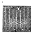
ガラス製シャーレに上記電解溶液2ml入れ、液中に上記1で作製したシリコン基板を浸した。次に、プローバー(共和理研、K−157MP)を用い、基板上の金パッドに電源を接続した。図1に示した電極のうち、下に見える凹型電極が陰極・上に見える串状電極が正極になるように配置した。この状態で、電流をモニターしながら800mVの電圧をかけて1分間電気分解を行い、その後、速やかに基板をとりだして余計な溶液を拭き取った。基板が十分に乾いてから電子顕微鏡で観察すると、図2に示すように(EDT−TTF)4Br3(TIE)5の小さな単結晶が多数生成した。図3は、図2の矢印部分を拡大した写真であるが、単結晶が電極間を強固に橋渡ししている状態が確認できた。
4.導通チェック
図4に矢印で示した部分をレーザーにより焼き切り、左右の電極間に1Vのバイアス電圧を印加することにより、約50nAの電流が流れることを確認した。
実施例2
1.シリコン基板の作製
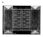
表面を酸化膜で覆ったシリコン基板にレジスト(PMMA/MMA)を塗布し、電子線リソグラフィー装置(エリオニクス7300)を使用して図5に示した回路を描画した。これを現像した後、50Åのチタン層、150Åの金層、100Åの銅層を蒸着した。さらに、アセトンでリフトオフを行った。このようにして、図5に示した電極層を作製した。
2.溶液の調整
20mlのアセトニトリルに対して、ジメチル−N,N’−ジシアノキノンジイミン(DMe−DCNQI)(Aldrich社製)を15mg加えてよく攪拌した。
3.単結晶の作製
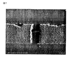
ガラス製シャーレに上記溶液を2ml入れ、液中に上記1で作製したシリコン基板を、30秒間浸した。顕微鏡観察により、基板上に微結晶が生成するのが観察できるので、適切な密度の結晶が成長したところで基板を引き上げ、乾燥させた。図6に示すように、単結晶が生成していることが確認された。図7は、図6の部分拡大写真であるが、単結晶が電極間を強固に橋渡ししている状態が確認できた。
4.導通チェック
上記で作製した回路を適宜レーザーにより焼き切って、導通チェックをしたところ、電流が流れることを確認した。例として図8に示すような4端子回路を作製し測定を行ったところ、結晶の抵抗が5kΩ、電極との接触抵抗が1kΩ程度の値を示した。The present invention will be described more specifically with reference to the following examples. The materials, amounts used, ratios, processing details, processing procedures, and the like shown in the following examples can be changed as appropriate without departing from the spirit of the present invention. Therefore, the scope of the present invention is not limited to the specific examples shown below.
Example 1
1. Production of electrode layer A positive resist (ZEP) is applied to a silicon substrate (manufacturer: Furuuchi Chemical) whose surface is covered with an oxide film, and the circuit shown in FIG. 1 is drawn using an electron beam lithography apparatus (Elionix 7300). did. This was developed with pentyl acetate, and then a 50Å titanium layer, a 1500Å gold layer, and a 20Å silicon dioxide layer were deposited. Furthermore, lift-off was performed with 2-butanone. Thus, the electrode layer shown in FIG. 1 was produced.
2. Preparation of electrolytic solution For 18 ml of chlorobenzene, Chem. Lett, vol. 1989, p781 EDT-TTF 12 mg, tetraphenylphosphonium bromide (Tokyo Kasei, T1069) 20 mg, tetraiodoethylene (TIE) (Aldrich, 31824-8) 80 mg, methanol 2 ml may be added and stirred And left overnight.
3. Preparation of single crystal by electrolysis 2 ml of the electrolytic solution was placed in a glass petri dish, and the silicon substrate prepared in 1 was immersed in the liquid. Next, a power source was connected to the gold pad on the substrate using a prober (Kyowa Riken, K-157MP). Among the electrodes shown in FIG. 1, the concave electrode visible below is the cathode and the skewer electrode visible above is the positive electrode. In this state, electrolysis was performed for 1 minute by applying a voltage of 800 mV while monitoring the current, and then the substrate was quickly taken out to wipe off the excess solution. When the substrate was sufficiently dried and observed with an electron microscope, many single crystals of (EDT-TTF) 4 Br 3 (TIE) 5 were formed as shown in FIG. FIG. 3 is an enlarged photograph of the arrow portion in FIG. 2, and it was confirmed that the single crystal firmly bridges the electrodes.
4). Continuity check It was confirmed that a current of about 50 nA flows by burning out a portion indicated by an arrow in FIG. 4 with a laser and applying a bias voltage of 1 V between the left and right electrodes.
Example 2
1. Production of Silicon Substrate A resist (PMMA / MMA) was applied to a silicon substrate whose surface was covered with an oxide film, and the circuit shown in FIG. 5 was drawn using an electron beam lithography apparatus (Elionix 7300). After developing this, a 50 チ タ ン titanium layer, a 150 金 gold layer, and a 100 銅 copper layer were deposited. Further, lift-off was performed with acetone. In this way, the electrode layer shown in FIG. 5 was produced.
2. Preparation of Solution 15 mg of dimethyl-N, N′-dicyanoquinonediimine (DMe-DCNQI) (Aldrich) was added to 20 ml of acetonitrile and stirred well.
3. Preparation of Single Crystal 2 ml of the above solution was placed in a glass petri dish, and the silicon substrate prepared in 1 above was immersed in the liquid for 30 seconds. Since microcrystals can be observed on the substrate by microscopic observation, the substrate was pulled up and dried when crystals of an appropriate density were grown. As shown in FIG. 6, it was confirmed that a single crystal was generated. FIG. 7 is a partially enlarged photograph of FIG. 6, and it was confirmed that the single crystal firmly bridges the electrodes.
4). Continuity check The circuit produced above was burned out with a laser as appropriate, and a continuity check was performed. As an example, a four-terminal circuit as shown in FIG. 8 was prepared and measured, and the resistance of the crystal was 5 kΩ and the contact resistance with the electrode was about 1 kΩ.
本発明では、一対の電極に、有機化合物からなる単結晶を作製することに成功し、電極間の導通を実現できた。従来、有機化合物からなる導体以外で構成された素子や多結晶の素子は知られていたものの、本発明のように単結晶の有機化合物からなる導体を含む素子については、全く得られていなかった。また、単結晶の有機化合物からなる導体の実験方法等についても、全く不明であった。
しかしながら、発明者の鋭意検討により、今回、このような素子の完成ができた。これは、きわめて偉大なものである。
加えて、後述するとおり、本発明の素子では、伝導性を、単結晶を1つについてだけ測定すること可能となったため、素子間でのばらつき等を防ぐことが可能となった。結果として、動作性能のより向上を図ることが可能となった。
さらに、本発明の方法では、ガラス基板の上ではなく、シリコン基板等の上にも作製できるので、分子性導体に対して、ゲート電極も含めた回路の作製を可能となった。
さらにまた、単結晶の有機化合物からなる導体では構成要素が「分子」であるため、様々な機能性をもった官能基を導入することが可能であり、従来の無機系デバイスとは異なる特性の発現が期待できる。特に、素子が単結晶という非常に構造的にクリーンな系であるため、高感度・高精密なデバイス特性が期待でき、広い範囲にわたって応用が期待できる。
さらに本発明の方法は、電極上に直接単結晶を生成させることができるので、従来行われていた絶縁膜をスパッタリングで接合させる手法に比べると、用いるシリコン基板の表面を平滑にしておけばその形に合わせて結晶が成長するので、非常に平面性の高い接合が形成できる。従って、有機化合物からなる導体を素子として粒界の影響なしに利用する道が開かれた。
本発明の素子は、高速応答が可能な薄膜トランジスタあるいは、光、湿度またはpH等に反応する高感度センサに利用することができる。さらに、単結晶を並列させた(好ましくは、1000個以上)素子を採用することにより、より微弱な信号の検出も可能なセンサに利用することができる。In the present invention, a single crystal made of an organic compound was successfully produced on a pair of electrodes, and conduction between the electrodes could be realized. Conventionally, elements composed of conductors other than organic compounds and polycrystalline elements have been known, but no element including a conductor composed of a single crystal organic compound as in the present invention has been obtained. . In addition, the experimental method of conductors made of single crystal organic compounds was completely unknown.
However, due to the inventor's earnest examination, such an element has been completed this time. This is extremely great.
In addition, as will be described later, in the element of the present invention, it is possible to measure the conductivity of only one single crystal, and thus it is possible to prevent variations among elements. As a result, it is possible to further improve the operation performance.
Furthermore, since the method of the present invention can be produced not only on a glass substrate but also on a silicon substrate or the like, a circuit including a gate electrode can be produced for a molecular conductor.
Furthermore, since the constituent element of a conductor made of a single crystal organic compound is a “molecule”, it is possible to introduce functional groups having various functionalities and have characteristics different from those of conventional inorganic devices. Expression can be expected. In particular, since the element is a very structurally clean system in which a single crystal is used, high sensitivity and high precision device characteristics can be expected, and application can be expected over a wide range.
Furthermore, since the method of the present invention can generate a single crystal directly on the electrode, compared with the conventional method of joining an insulating film by sputtering, the surface of the silicon substrate to be used can be made smooth. Since the crystal grows in accordance with the shape, a very flat junction can be formed. Therefore, the path | route which utilizes the conductor which consists of an organic compound as an element without the influence of a grain boundary was opened.
The element of the present invention can be used for a thin film transistor capable of high-speed response or a highly sensitive sensor that reacts to light, humidity, pH, or the like. Furthermore, by employing an element in which single crystals are arranged in parallel (preferably 1000 or more), it can be used for a sensor capable of detecting a weaker signal.
Claims (10)
いずれも正極または負極である一対の電極を電解溶液に浸漬し、前記一対の電極に電圧をかけて、前記電解溶液を電気分解することにより、前記一対の電極間に単結晶の有機化合物からなる導体を形成する工程を含む、素子の製造方法。 A method for producing an element comprising a pair of electrodes having a distance between electrodes of 10 to 900 nm and a conductor made of a single crystal organic compound provided between the electrodes ,
A pair of electrodes, each of which is a positive electrode or a negative electrode, is immersed in an electrolytic solution, a voltage is applied to the pair of electrodes, and the electrolytic solution is electrolyzed to form a single crystal organic compound between the pair of electrodes. An element manufacturing method including a step of forming a conductor.
Priority Applications (1)
| Application Number | Priority Date | Filing Date | Title |
|---|---|---|---|
| JP2006512642A JP4878552B2 (en) | 2004-04-20 | 2005-04-20 | Device, thin film transistor and sensor using the same, and device manufacturing method |
Applications Claiming Priority (4)
| Application Number | Priority Date | Filing Date | Title |
|---|---|---|---|
| JP2004123757 | 2004-04-20 | ||
| JP2004123757 | 2004-04-20 | ||
| PCT/JP2005/007945 WO2005104260A1 (en) | 2004-04-20 | 2005-04-20 | Element, thin film transistor and sensor using the same, and method for manufacture of element |
| JP2006512642A JP4878552B2 (en) | 2004-04-20 | 2005-04-20 | Device, thin film transistor and sensor using the same, and device manufacturing method |
Publications (2)
| Publication Number | Publication Date |
|---|---|
| JPWO2005104260A1 JPWO2005104260A1 (en) | 2008-03-13 |
| JP4878552B2 true JP4878552B2 (en) | 2012-02-15 |
Family
ID=35197288
Family Applications (1)
| Application Number | Title | Priority Date | Filing Date |
|---|---|---|---|
| JP2006512642A Expired - Fee Related JP4878552B2 (en) | 2004-04-20 | 2005-04-20 | Device, thin film transistor and sensor using the same, and device manufacturing method |
Country Status (4)
| Country | Link |
|---|---|
| US (1) | US20080017400A1 (en) |
| JP (1) | JP4878552B2 (en) |
| TW (1) | TW200607099A (en) |
| WO (1) | WO2005104260A1 (en) |
Families Citing this family (1)
| Publication number | Priority date | Publication date | Assignee | Title |
|---|---|---|---|---|
| CN102583235B (en) * | 2012-03-22 | 2015-07-22 | 中国科学院化学研究所 | Method for preparing organic micro/nano structure by liquid phase chemical reaction method and patterning in situ |
Citations (4)
| Publication number | Priority date | Publication date | Assignee | Title |
|---|---|---|---|---|
| JPS636872A (en) * | 1986-06-27 | 1988-01-12 | Canon Inc | Negative resistance element |
| JPH0279401A (en) * | 1988-09-14 | 1990-03-20 | Mitsubishi Petrochem Co Ltd | Nonlinear electric conduction element |
| JPH06321686A (en) * | 1993-03-15 | 1994-11-22 | Wako Pure Chem Ind Ltd | New production of carbon cluster compound doped with metal atom |
| WO2003076332A1 (en) * | 2002-03-08 | 2003-09-18 | Communications Research Laboratory, Independent Administrative Institution | Production device and production method for conductive nano-wire |
Family Cites Families (4)
| Publication number | Priority date | Publication date | Assignee | Title |
|---|---|---|---|---|
| JPS63305188A (en) * | 1987-06-06 | 1988-12-13 | Sony Corp | Display material |
| FR2843742B1 (en) * | 2002-08-26 | 2005-10-14 | Commissariat Energie Atomique | MICROSTRUCTURE WITH FUNCTIONALIZED SURFACE BY LOCALIZED DEPOSITION OF A THIN LAYER AND METHOD OF MANUFACTURING THE SAME |
| JP4774679B2 (en) * | 2004-03-31 | 2011-09-14 | 大日本印刷株式会社 | Organic semiconductor device |
| US7477013B2 (en) * | 2004-08-12 | 2009-01-13 | E. I. Du Pont De Nemours And Company | Organic light emitting devices with distinct resistance regions |
-
2005
- 2005-04-20 US US11/587,129 patent/US20080017400A1/en not_active Abandoned
- 2005-04-20 TW TW094112591A patent/TW200607099A/en unknown
- 2005-04-20 WO PCT/JP2005/007945 patent/WO2005104260A1/en not_active Ceased
- 2005-04-20 JP JP2006512642A patent/JP4878552B2/en not_active Expired - Fee Related
Patent Citations (4)
| Publication number | Priority date | Publication date | Assignee | Title |
|---|---|---|---|---|
| JPS636872A (en) * | 1986-06-27 | 1988-01-12 | Canon Inc | Negative resistance element |
| JPH0279401A (en) * | 1988-09-14 | 1990-03-20 | Mitsubishi Petrochem Co Ltd | Nonlinear electric conduction element |
| JPH06321686A (en) * | 1993-03-15 | 1994-11-22 | Wako Pure Chem Ind Ltd | New production of carbon cluster compound doped with metal atom |
| WO2003076332A1 (en) * | 2002-03-08 | 2003-09-18 | Communications Research Laboratory, Independent Administrative Institution | Production device and production method for conductive nano-wire |
Also Published As
| Publication number | Publication date |
|---|---|
| JPWO2005104260A1 (en) | 2008-03-13 |
| US20080017400A1 (en) | 2008-01-24 |
| TW200607099A (en) | 2006-02-16 |
| WO2005104260A1 (en) | 2005-11-03 |
Similar Documents
| Publication | Publication Date | Title |
|---|---|---|
| Di et al. | High-performance organic field-effect transistors: Molecular design, device fabrication, and physical properties | |
| Letizia et al. | High electron mobility in solution-cast and vapor-deposited phenacyl− quaterthiophene-based field-effect transistors: toward n-type polythiophenes | |
| Liu et al. | Critical impact of gate dielectric interfaces on the contact resistance of high-performance organic field-effect transistors | |
| Mas-Torrent et al. | Correlation between crystal structure and mobility in organic field-effect transistors based on single crystals of tetrathiafulvalene derivatives | |
| Hicks et al. | Synthesis and Electronic Structure Investigations of α, ω-Bis (arylthio) oligothiophenes: Toward Understanding Wire-Linker Interactions in Molecular-Scale Electronic Materials | |
| Yuan et al. | Chemical control over the energy-level alignment in a two-terminal junction | |
| CN102867914B (en) | The manufacture method of electronic device and semiconductor devices | |
| US20120018706A1 (en) | Organic semiconductors capable of ambipolar transport | |
| Sarkar et al. | Resistive switching of the tetraindolyl derivative in ultrathin films: a potential candidate for nonvolatile memory applications | |
| US8120018B2 (en) | Semiconductor device comprising semiconductor molecules and a conductor formed of fine particles and linker molecules | |
| US20140291659A1 (en) | Dioxaanthanthrene compound, laminated structure and formation method thereof, and electronic device and manufacturing method thereof | |
| Mukherjee et al. | High performance organic thin film transistors with solution processed TTF-TCNQ charge transfer salt as electrodes | |
| JP2006005330A (en) | Thin film transistor array panel and manufacturing method thereof | |
| JP2004179249A (en) | Organic semiconductor material, organic electronic device using the same, and method of manufacturing organic electronic device | |
| JP4878552B2 (en) | Device, thin film transistor and sensor using the same, and device manufacturing method | |
| US10256407B2 (en) | Organic thin film transistors | |
| Videlot-Ackermann et al. | Influence of phenyl perfluorination on charge transport properties of distyryl-oligothiophenes in organic field-effect transistors | |
| Sun et al. | Improved morphology and performance from surface treatments of naphthalenetetracarboxylic diimide bottom contact field-effect transistors | |
| JP2006005036A (en) | Organic compound crystal and field effect transistor | |
| WO2011052285A1 (en) | Novel compound, field-effective transistor, solar cell, method for producing said compound, field-effective transistor, and solar cell, composition for organic semiconductor layer, and composition for p-type semiconductor layer | |
| JP5031584B2 (en) | Organic thin film transistor | |
| JP6326297B2 (en) | Electrode for organic device and organic device provided with the same | |
| KR20080103893A (en) | Organic Semiconductor Devices and Organic Semiconductor Thin Films | |
| JP2006278692A (en) | Organic field effect transistor | |
| JP4639703B2 (en) | Electronic device manufacturing method and semiconductor device manufacturing method |
Legal Events
| Date | Code | Title | Description |
|---|---|---|---|
| A621 | Written request for application examination |
Free format text: JAPANESE INTERMEDIATE CODE: A621 Effective date: 20080416 |
|
| A521 | Request for written amendment filed |
Free format text: JAPANESE INTERMEDIATE CODE: A523 Effective date: 20080416 |
|
| A131 | Notification of reasons for refusal |
Free format text: JAPANESE INTERMEDIATE CODE: A131 Effective date: 20110906 |
|
| A521 | Request for written amendment filed |
Free format text: JAPANESE INTERMEDIATE CODE: A523 Effective date: 20111020 |
|
| TRDD | Decision of grant or rejection written | ||
| A01 | Written decision to grant a patent or to grant a registration (utility model) |
Free format text: JAPANESE INTERMEDIATE CODE: A01 Effective date: 20111122 |
|
| A01 | Written decision to grant a patent or to grant a registration (utility model) |
Free format text: JAPANESE INTERMEDIATE CODE: A01 |
|
| A61 | First payment of annual fees (during grant procedure) |
Free format text: JAPANESE INTERMEDIATE CODE: A61 Effective date: 20111128 |
|
| R150 | Certificate of patent or registration of utility model |
Free format text: JAPANESE INTERMEDIATE CODE: R150 |
|
| FPAY | Renewal fee payment (event date is renewal date of database) |
Free format text: PAYMENT UNTIL: 20141209 Year of fee payment: 3 |
|
| R250 | Receipt of annual fees |
Free format text: JAPANESE INTERMEDIATE CODE: R250 |
|
| S533 | Written request for registration of change of name |
Free format text: JAPANESE INTERMEDIATE CODE: R313533 |
|
| R350 | Written notification of registration of transfer |
Free format text: JAPANESE INTERMEDIATE CODE: R350 |
|
| R250 | Receipt of annual fees |
Free format text: JAPANESE INTERMEDIATE CODE: R250 |
|
| LAPS | Cancellation because of no payment of annual fees |