JP2005294660A - Semiconductor device substrate and manufacturing method thereof - Google Patents
Semiconductor device substrate and manufacturing method thereof Download PDFInfo
- Publication number
- JP2005294660A JP2005294660A JP2004109656A JP2004109656A JP2005294660A JP 2005294660 A JP2005294660 A JP 2005294660A JP 2004109656 A JP2004109656 A JP 2004109656A JP 2004109656 A JP2004109656 A JP 2004109656A JP 2005294660 A JP2005294660 A JP 2005294660A
- Authority
- JP
- Japan
- Prior art keywords
- substrate
- wiring pattern
- wiring
- semiconductor device
- wiring patterns
- Prior art date
- Legal status (The legal status is an assumption and is not a legal conclusion. Google has not performed a legal analysis and makes no representation as to the accuracy of the status listed.)
- Granted
Links
Images

Landscapes
- Production Of Multi-Layered Print Wiring Board (AREA)
Abstract
Description
本発明は、複数の配線層からなり、薄型で高密度配線を有する半導体装置用基板に関する。 The present invention relates to a semiconductor device substrate comprising a plurality of wiring layers and having thin and high density wiring.
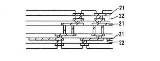
電子技術の進歩に伴い、電子情報端末の小型化、軽量化、高機能化がますます求められてきており、このため、半導体装置用基板においても、高密度化が強く求められている。従来、半導体装置用基板は、絶縁層と配線パターンが交互に繰り返された構造を有しているが、各層にある配線パターン間の電気的接続方法は、スルーホールもしくはビアホール等を介してなされている。即ち、断面構造は「配線層21(配線パターンとその周囲の絶縁物)」と「絶縁層22(絶縁物とビアホール)」を交互に積み重ねた構造、つまり、配線パターンが形成された配線層と、上下の配線パターンに対応して配置されたφ50〜150μm前後の円形パターンのみで構成されるビアホールが形成された絶縁層を交互に積み重ねた構造となっている(図1参照)。 Along with the advancement of electronic technology, there is an increasing demand for miniaturization, weight reduction, and high functionality of electronic information terminals. For this reason, high density is also strongly demanded for semiconductor device substrates. Conventionally, a substrate for a semiconductor device has a structure in which an insulating layer and a wiring pattern are alternately repeated. However, an electrical connection method between wiring patterns in each layer is made through a through hole or a via hole. Yes. That is, the cross-sectional structure is a structure in which “wiring layer 21 (wiring pattern and insulator around it)” and “insulating layer 22 (insulator and via hole)” are alternately stacked, that is, the wiring layer on which the wiring pattern is formed and In this structure, insulating layers having via holes formed only by circular patterns having a diameter of about 50 to 150 μm arranged corresponding to the upper and lower wiring patterns are alternately stacked (see FIG. 1).
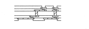
また、通常の多層基板やビルドアップ多層基板以外に、全層IVH構造の基板も知られている。この構造の基板には各種プロセスが提案されており、絶縁層となるプリプレグをレーザーで穿孔し、導電ペーストを充填した後、表裏に導箔を重ねて銅張積層板形成と同様なプロセスで表面が銅箔で覆われた素材を形成し、表面の導箔をエッチングして配線パターンを形成するもの(特許文献1〜3)や、銅箔にとげ状の導電ペーストを印刷し、加熱硬化後にプリプレグと通常の銅箔を重ねて銅張積層板形成と同様なプロセスで表面が銅箔で覆われた素材を形成し、表面の導箔をエッチングして配線パターンを形成するもの(特許文献4)や、これと類似の技術が多数知られている(図2参照)。 In addition to a normal multilayer substrate and a buildup multilayer substrate, a substrate having an all-layer IVH structure is also known. Various processes have been proposed for substrates with this structure. After prepregs that serve as insulating layers are drilled with a laser and filled with a conductive paste, conductive foils are stacked on the front and back surfaces in the same process as copper-clad laminates. After forming a material covered with copper foil, etching the conductive foil on the surface to form a wiring pattern (Patent Documents 1 to 3), or printing a spine-shaped conductive paste on the copper foil, after heat curing A prepreg and normal copper foil are stacked to form a material whose surface is covered with copper foil by a process similar to that for forming a copper-clad laminate, and a conductive pattern on the surface is etched to form a wiring pattern (Patent Document 4) ) And many similar techniques are known (see FIG. 2).
最近では、特殊な網目状の基材に感光剤を塗布し、露光した部位を活性化して無電解銅めっきを行うことで上下が貫通した導電部と非導電部を選択的に形成し、その表面に配線パターンを形成する技術が発表されている(非特許文献1)。
しかし、いずれの技術も導電部(ビアホール)を形成した絶縁層を基本として、その表面に配線パターンを形成し、配線層と絶縁層(+ビアホール)を交互に積み重ねる構造には変わりない。
Recently, a photosensitive agent is applied to a special mesh substrate, and the exposed part is activated and electroless copper plating is performed to selectively form a conductive part and a non-conductive part penetrating vertically. A technique for forming a wiring pattern on the surface has been announced (Non-Patent Document 1).
However, any of these techniques is based on an insulating layer in which conductive portions (via holes) are formed, and a wiring pattern is formed on the surface, and the wiring layers and insulating layers (+ via holes) are alternately stacked.
従来技術においては、上下の配線パターン間を接続するためのビアホールを形成する場合、ビアホール径は通常φ100〜200μm程度で、ビアホールを受けるための上下のビアランドはそれより50〜100μm大きなサイズが必要だった。例えば、ビアホールがφ150μmとすると、ビアランドの寸法はそれより60μm大きな210μmになる。 In the prior art, when forming a via hole for connecting the upper and lower wiring patterns, the diameter of the via hole is usually about φ100 to 200 μm, and the upper and lower via lands for receiving the via hole need to be 50 to 100 μm larger than that. It was. For example, if the via hole has a diameter of 150 μm, the via land size is 210 μm, which is 60 μm larger than that.
これに対し、同じ技術レベルのプロセスを用いても配線パターンは100μm前後のピッチでの形成が可能で、配線パターン内にビアランドが存在すると、3本の配線が並んだ部分をビアランドが占めてしまい、配線密度が極端に低下する。また、より高密度を要求する製品にはUVレーザーでビアホールを形成するプロセスが知られており、この場合にはφ50μm程度までのビアが形成可能になっている。ビア径がφ50μmの場合、ビアランド寸法は約110μmになり、それでも1〜2本の配線を阻害することになる。 On the other hand, the wiring pattern can be formed with a pitch of about 100 μm even if the process of the same technical level is used, and if the via land exists in the wiring pattern, the via land occupies the portion where the three wirings are arranged. Wiring density is extremely reduced. Further, a process for forming a via hole with a UV laser is known for products requiring higher density. In this case, a via having a diameter of up to about 50 μm can be formed. When the via diameter is 50 μm, the via land size is about 110 μm, which still inhibits one or two wires.
このように、ビアホールが配線パターンの高密度化に大きく影響するため、ビアホールの更なる微細化とビアランド寸法とビア径との差の縮小が望まれている。しかし、φ50μm程度かそれ以下のビア径では安定してビアを穿孔することが難しく、ビアのめっきに
ついては前処理も含めて更に困難な状況となっている。
As described above, since the via hole greatly affects the high density of the wiring pattern, further miniaturization of the via hole and reduction of the difference between the via land size and the via diameter are desired. However, if the diameter of the via is about 50 μm or less, it is difficult to stably drill the via, and the plating of the via is further difficult including the pretreatment.
以上については、ビアホールを形成する場合の技術的課題だが、レーザー加工装置などのビアを形成するための設備が配線パターン形成設備以外に必要なことなど、設備的な問題も含んでいる。
本発明は、上記問題を解決するためになされたものであり、レーザー加工装置などのビアを形成するための設備を用いずに、配線パターンの接続部の更なる微細化を可能とした、薄型で高密度な配線パターンを有する半導体装置用基板を提供することを課題とするものである。
また、上記半導体装置用基板の製造方法を提供することを課題とする。
The present invention has been made in order to solve the above-mentioned problem, and enables thinning of the connection portion of the wiring pattern without using a facility for forming a via such as a laser processing apparatus. An object of the present invention is to provide a semiconductor device substrate having a high-density wiring pattern.
It is another object of the present invention to provide a method for manufacturing the semiconductor device substrate.
即ち、請求項1記載の発明においては、少なくとも、上下に隣接する配線層の上下配線パターンが直接積み重なる構造の接続部と、該上下配線パターンが接続部以外では接触、又は必要な絶縁抵抗値以下の間隔に近接しないように配設した複数の配線層を有することを特徴とする半導体装置用基板としたものである。
これは、上述のように配線パターンどうしを直接積み重ねる接続部を設けることと、これによる隣接する配線層の配線パターンの短絡または配線パターンどうしが必要以上に近接することによる絶縁性の低下を防ぐように考慮した配線パターンを有する半導体装置用基板としたものである。
That is, in the first aspect of the present invention, at least the connection part of the structure in which the upper and lower wiring patterns of the wiring layers adjacent to each other are directly stacked, and the upper and lower wiring patterns are in contact with each other except the connection part or less than the required insulation resistance value A substrate for a semiconductor device having a plurality of wiring layers arranged so as not to be close to each other.
This is to prevent the deterioration of the insulation due to the provision of the connection portion for directly stacking the wiring patterns as described above, and the shorting of the wiring patterns of the adjacent wiring layers or the close proximity of the wiring patterns. This is a substrate for a semiconductor device having a wiring pattern considering the above.
また、請求項2記載の発明においては、前記上下配線パターンは、厚みが3〜35μmの金属又は導電性有機材料からなり、該上下配線パターンと略同一平面上の上下配線パターン周囲が絶縁物で覆われた層を有することを特徴とする半導体装置用基板としたものである。
これは、上記請求項1の発明のうち、半導体装置用基板で使用される市販の銅箔に相当する配線パターン厚みに限定した金属とそれに代わりうる導電性有機材料を用い、配線パターン以外の部分が樹脂で充填されて略同一平面を成す構造の層を少なくとも1層以上含んだ構造としたものである。
According to a second aspect of the present invention, the upper and lower wiring patterns are made of metal or a conductive organic material having a thickness of 3 to 35 μm, and the periphery of the upper and lower wiring patterns on the same plane as the upper and lower wiring patterns is an insulator. A substrate for a semiconductor device, characterized by having a covered layer.
This is a part other than the wiring pattern, using a metal limited to a wiring pattern thickness corresponding to a commercially available copper foil used in a substrate for a semiconductor device and a conductive organic material that can be substituted for it, in the invention of claim 1. Are filled with resin and have a structure including at least one layer having a substantially identical plane.
また、請求項3記載の発明においては、(1)平坦なベース基板上に配線パターン(P1)とその周囲の絶縁物を表面が略同一平面状となるように形成する工程と、(2)次の配線パターン(P2)を上記配線パターン(P1)上に直接積み重ねて形成し接続部を設け、該配線パターン(P2)の周囲の絶縁物を表面が略同一平面状となるように形成する工程と、(3)上記(2)工程を必要な層数分繰り返す工程、を少なくとも有することを特徴とする半導体装置用基板の製造方法としたものである。
これは、平坦なベース基板上に配線パターンとその周囲を充填するような絶縁物をほぼ同じ厚みで形成し、表面が略同一平面となるように形成し、それを必要な層数だけ重ねることによって、所望の半導体装置用基板を得るための製造方法である。
According to a third aspect of the present invention, (1) a step of forming a wiring pattern (P1) and an insulating material around the wiring pattern (P1) on a flat base substrate so that the surfaces are substantially flush with each other; The next wiring pattern (P2) is formed by directly stacking on the wiring pattern (P1) to provide a connection portion, and the insulator around the wiring pattern (P2) is formed so that the surface is substantially flush. A method of manufacturing a substrate for a semiconductor device, comprising at least a step and (3) a step of repeating the step (2) above for the required number of layers.
This is because an insulating material that fills the wiring pattern and its surroundings is formed on a flat base substrate with approximately the same thickness, and the surface is formed to be substantially flush with the required number of layers. Is a manufacturing method for obtaining a desired substrate for a semiconductor device.
また、請求項4記載の発明においては、前記(3)工程後に、平坦なベース基板の少なくとも一部を除去する工程を有することを特徴とする半導体装置用基板の製造方法としたものである。 According to a fourth aspect of the present invention, there is provided a method for manufacturing a substrate for a semiconductor device, comprising a step of removing at least a part of a flat base substrate after the step (3).
また、請求項5記載の発明においては、前記平坦なベース基板が50〜700μmの厚みの金属板、ガラス板、プラスチック板、又はシリコン基板であることを特徴とする半導体装置用基板の製造方法としたものである。
これは、微細パターン形成に適した平滑で入手が容易な半導体用や表示装置用などに使用されるベース基板材料とその一般的な厚みについて規定したものである。
According to a fifth aspect of the present invention, there is provided a method of manufacturing a substrate for a semiconductor device, wherein the flat base substrate is a metal plate, glass plate, plastic plate, or silicon substrate having a thickness of 50 to 700 μm. It is a thing.
This stipulates the base substrate material used for smooth and easily available semiconductors and display devices suitable for fine pattern formation and its general thickness.
本発明の半導体装置用基板は、接続部の構造が上下に隣接する配線層の上下配線パターンが直接積み重なる構造であるので、多層部に従来のビアホール(スルーホールやブラインドホール)を介さないで層間接続が可能なことから、超薄型で高密度配線を有する半導体装置用基板となる。 The substrate for a semiconductor device according to the present invention has a structure in which the upper and lower wiring patterns of the wiring layers adjacent to each other in the upper and lower sides are directly stacked, so that the multilayer portion does not include a conventional via hole (through hole or blind hole). Since connection is possible, the substrate for a semiconductor device having ultra-thin and high-density wiring is obtained.
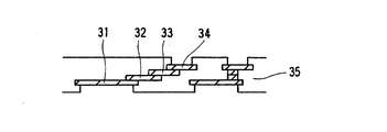
本発明者は、鋭意検討の結果、上記のような従来の問題を解決することができた。図3は、本発明による半導体装置用基板の一例の断面図である。図3に示すように、半導体装置用基板の接続部は、上下に隣接する配線層の上下配線パターン(31〜34)が相互に直接積み重なる構造となっている。また、上下配線パターンは接続部以外では接触、又は必要な絶縁抵抗値以下の間隔に近接しないよう配設されている。
すなわち、従来のビアホール(スルーホールやブラインドホール)が必要ないことから、薄型で高密度配線を有する半導体装置用基板となる。
As a result of intensive studies, the present inventor has been able to solve the conventional problems as described above. FIG. 3 is a cross-sectional view of an example of a substrate for a semiconductor device according to the present invention. As shown in FIG. 3, the connection part of the substrate for a semiconductor device has a structure in which upper and lower wiring patterns (31 to 34) of wiring layers adjacent to each other are directly stacked. In addition, the upper and lower wiring patterns are arranged so as not to be in contact with each other except for the connection portion or to be close to an interval equal to or less than a necessary insulation resistance value.
That is, since a conventional via hole (through hole or blind hole) is not required, the semiconductor device substrate is thin and has high-density wiring.
以下に、実施例に基づき、本発明をさらに具体的に説明するが、これに限定されるものではない。 Hereinafter, the present invention will be described more specifically based on examples, but is not limited thereto.
(4層配線基板の作成)
表裏に、第2層の配線パターン2及び第3層の配線パターン3が形成され、かつ、表裏がビアホール1で導通せしめてなる2層配線基板(図4(a))の両面に、絶縁性フィルム(ABF−70H(商品名)、味の素ファインテクノ(株)製)をラミネートし、140℃で60分間加熱して樹脂を硬化させた。この絶縁性フィルム表面を、両面ともバフによる物理研磨により、第2層、第3層の配線パターンの銅表面が露出するまで研磨を行った(図4(b))。
(Creation of 4-layer wiring board)
The second
次に、過マンガン酸処理を行って、絶縁性フィルム表面を両面とも粗化した後、無電解銅めっきを行いシード層4を形成した(図4(c))。その後、両面に厚みが20μmのドライフィルム(サンフォートAQ−2058(商品名)、旭化成(株)製)をラミネートし、平行光型の露光機で、それぞれ第1層と第4層の配線パターンを焼付け、1%炭酸ナトリウム溶液で現像し、ドライフィルムのパターン5を得た(図4(d))。その後、電解めっきにより配線パターン部をめっきした後(図4(e))、ドライフィルムを剥離し(図4(f))、フラッシュエッチングにより、シード層を除去することで、第1層の配線パターン6及び第4層の配線パターン7を形成した(図4(g))。
Next, after permanganic acid treatment was performed to roughen both surfaces of the insulating film, electroless copper plating was performed to form a seed layer 4 (FIG. 4C). Thereafter, a dry film (Sunfort AQ-2058 (trade name), manufactured by Asahi Kasei Co., Ltd.) having a thickness of 20 μm is laminated on both sides, and the first and fourth layer wiring patterns are respectively formed with a parallel light type exposure machine. The film was baked and developed with a 1% sodium carbonate solution to obtain a dry film pattern 5 (FIG. 4D). Thereafter, after plating the wiring pattern portion by electrolytic plating (FIG. 4E), the dry film is peeled off (FIG. 4F), and the seed layer is removed by flash etching, thereby forming the first layer wiring. A
この両面にこれまでと同様にして、絶縁性フィルム(ABF−70H(商品名)、味の素ファインテクノ(株)製)をラミネートし、140℃で60分間加熱して樹脂を硬化させ、両面とも表面をバフによる物理研磨により、第1層、第4層の配線パターンの銅表面が露出するまで研磨を行い、4層配線を有する多層回路基板を作成した(図4(h))。 Insulating films (ABF-70H (trade name), manufactured by Ajinomoto Fine Techno Co., Ltd.) are laminated on both sides in the same manner as before, and the resin is cured by heating at 140 ° C. for 60 minutes. Was polished until the copper surfaces of the wiring patterns of the first layer and the fourth layer were exposed by buffing, and a multilayer circuit board having a four-layer wiring was produced (FIG. 4 (h)).
(放熱板付き3層配線基板の作成)
厚みが100μmのジルコニウム系銅板8(C151(商品名)、三菱伸銅(株)製、CDA合金NO.C15100)(図5(a))の両面に、厚みが20μmのドライフィルム9(サンフォートAQ−2058(商品名)、旭化成(株)製)をラミネートし、平行光型の露光機で一方の面に配線パターンのネガパターンを焼付け、もう片方の面は全面露光を行った後、1%炭酸ナトリウム溶液で現像を行った後(図5(b))、電解めっきを約15μm行い、3%水酸化ナトリウム溶液でドライフィルムを剥離し、第3層の配線パターン10を形成した(図5(c))。
(Making a three-layer wiring board with a heat sink)
Zirconium-based
次に、第3層の配線パターンを形成した側に絶縁性フィルム(ABF−70H(商品名)、味の素ファインテクノ(株)製)をラミネートし、140℃で60分間加熱して樹脂を硬化させた。この絶縁性フィルム表面をバフによる物理研磨により、第3層の配線パターンの銅表面が露出するまで研磨を行った(図5(d))。
次に、過マンガン酸処理を行って、絶縁性フィルム表面を粗化した後、無電解銅めっきを行いシード層11を形成した(図5(e))。その後、第3層の配線パターンを形成したときと同様に、両面に厚みが20μmのドライフィルム(サンフォートAQ−2058(商品名)、旭化成(株)製)をラミネートし、平行光型の露光機で第3層の配線パターンがある面に第2層の配線パターンのネガパターンを焼付け、もう片方の面は全面露光を行った後、1%炭酸ナトリウム溶液で現像(図5(f))、電解めっき(図5(g))、ドライフィルムを剥離し、第2層の配線パターン12を形成した(図5(h))。この工程を繰り返すことにより第1層の配線パターン13を形成し、放熱板付き3層配線を有する多層回路基板を作成した(図5(j))。
Next, an insulating film (ABF-70H (trade name), manufactured by Ajinomoto Fine Techno Co., Ltd.) is laminated on the side on which the wiring pattern of the third layer is formed, and the resin is cured by heating at 140 ° C. for 60 minutes. It was. The insulating film surface was polished by buffing until the copper surface of the third layer wiring pattern was exposed (FIG. 5D).
Next, a permanganate treatment was performed to roughen the surface of the insulating film, and then electroless copper plating was performed to form a seed layer 11 (FIG. 5E). Thereafter, a dry film (Sunfort AQ-2058 (trade name), manufactured by Asahi Kasei Co., Ltd.) having a thickness of 20 μm is laminated on both surfaces in the same manner as when the third-layer wiring pattern is formed, and a parallel light type exposure is performed. The negative pattern of the second layer wiring pattern was printed on the surface having the third layer wiring pattern on the machine, and the other surface was exposed to the entire surface and developed with a 1% sodium carbonate solution (FIG. 5 (f)). Then, electrolytic plating (FIG. 5G), the dry film was peeled off, and a second
(超薄膜3層配線基板の作成)
実施例2で作成した放熱板付き3層配線を有する多層回路基板(図6(a))の配線層側の面を、厚みが20μmのドライフィルム(サンフォートAQ−2058(商品名)、旭化成(株)製)をラミネートすることで保護し、他方面のジルコニウム系銅板8をエッチングにより除去することで、超薄膜3層配線基板を作成した(図6(b))。
(Creation of ultra-thin three-layer wiring board)
The surface on the wiring layer side of the multilayer circuit board (FIG. 6 (a)) having a three-layer wiring with a heat sink created in Example 2 is a dry film (Sunfort AQ-2058 (trade name), Asahi Kasei Co., Ltd.) having a thickness of 20 μm. (Made by Co., Ltd.) was protected by laminating, and the zirconium-based
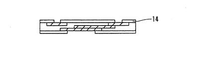
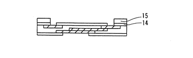
以上、実施例に基づき具体例を述べたが、これに限定されるものではない。また、本発明においては、必要に応じて、既存のソルダーレジスト14やカバーレイをコーティングする構成としても良く(図7)、さらに接続端子に金めっき、錫めっき、耐熱プリフラックス塗布などの防錆用の処理を施しても良い。また、ハンドリング性向上のため、スティフナー(補強板)15を搭載してもよい(図8)。 As mentioned above, although the specific example was described based on the Example, it is not limited to this. Moreover, in this invention, it is good also as a structure which coats the existing soldering resist 14 and coverlay as needed (FIG. 7), and also rust prevention, such as gold plating, tin plating, and heat-resistant preflux application | coating to a connection terminal You may perform the process for. Further, a stiffener (reinforcing plate) 15 may be mounted to improve handling properties (FIG. 8).
1・・・ビアホール
2、12・・・第2層の配線パターン
3、10・・・第3層の配線パターン
4、11・・・シード層
5・・・ドライフィルムのパターン
6、13・・・第1層の配線パターン
7・・・第4層の配線パターン
8・・・ジルコニウム系銅板
9・・・ドライフィルム
14…ソルダーレジスト
15…スティフナー
21・・・配線層
22・・・絶縁層
23・・・表面の導箔をエッチングして配線パターンを形成するもの
31、32、33、34・・・上下配線パターン
35・・・絶縁物
DESCRIPTION OF SYMBOLS 1 ... Via
Claims (5)
(2)次の配線パターン(P2)を上記配線パターン(P1)上に直接積み重ねて形成し接続部を設け、該配線パターン(P2)の周囲の絶縁物を表面が略同一平面状となるように形成する工程と、
(3)上記(2)工程を必要な層数分繰り返す工程、
を少なくとも有することを特徴とする半導体装置用基板の製造方法。 (1) forming a wiring pattern (P1) and an insulating material around the wiring pattern (P1) on a flat base substrate so that the surfaces thereof are substantially flush with each other;
(2) The next wiring pattern (P2) is formed by directly stacking on the wiring pattern (P1) to provide a connection portion, and the surface of the insulator around the wiring pattern (P2) is substantially flush. Forming the step,
(3) A step of repeating the above step (2) for the required number of layers,
The manufacturing method of the board | substrate for semiconductor devices characterized by having at least.
Priority Applications (1)
| Application Number | Priority Date | Filing Date | Title |
|---|---|---|---|
| JP2004109656A JP4466169B2 (en) | 2004-04-02 | 2004-04-02 | Manufacturing method of substrate for semiconductor device |
Applications Claiming Priority (1)
| Application Number | Priority Date | Filing Date | Title |
|---|---|---|---|
| JP2004109656A JP4466169B2 (en) | 2004-04-02 | 2004-04-02 | Manufacturing method of substrate for semiconductor device |
Publications (2)
| Publication Number | Publication Date |
|---|---|
| JP2005294660A true JP2005294660A (en) | 2005-10-20 |
| JP4466169B2 JP4466169B2 (en) | 2010-05-26 |
Family
ID=35327231
Family Applications (1)
| Application Number | Title | Priority Date | Filing Date |
|---|---|---|---|
| JP2004109656A Expired - Fee Related JP4466169B2 (en) | 2004-04-02 | 2004-04-02 | Manufacturing method of substrate for semiconductor device |
Country Status (1)
| Country | Link |
|---|---|
| JP (1) | JP4466169B2 (en) |
Cited By (2)
| Publication number | Priority date | Publication date | Assignee | Title |
|---|---|---|---|---|
| JP2008016817A (en) * | 2006-07-06 | 2008-01-24 | Samsung Electro-Mechanics Co Ltd | Buried pattern substrate and its manufacturing method |
| JP2013247355A (en) * | 2012-05-29 | 2013-12-09 | Zhuhai Advanced Chip Carriers & Electronic Substrates Solutions Technologies Co Ltd | Multilayer electronic structure with integral vias extending in in-plane direction |
-
2004
- 2004-04-02 JP JP2004109656A patent/JP4466169B2/en not_active Expired - Fee Related
Cited By (2)
| Publication number | Priority date | Publication date | Assignee | Title |
|---|---|---|---|---|
| JP2008016817A (en) * | 2006-07-06 | 2008-01-24 | Samsung Electro-Mechanics Co Ltd | Buried pattern substrate and its manufacturing method |
| JP2013247355A (en) * | 2012-05-29 | 2013-12-09 | Zhuhai Advanced Chip Carriers & Electronic Substrates Solutions Technologies Co Ltd | Multilayer electronic structure with integral vias extending in in-plane direction |
Also Published As
| Publication number | Publication date |
|---|---|
| JP4466169B2 (en) | 2010-05-26 |
Similar Documents
| Publication | Publication Date | Title |
|---|---|---|
| TWI271136B (en) | Flexible multi-layered wiring substrate and its manufacturing method | |
| JP5580135B2 (en) | Printed wiring board manufacturing method and printed wiring board | |
| JP2015122545A (en) | Multilayer wiring board and manufacturing method thereof | |
| JP2009260204A (en) | Printed circuit board and method of manufacturing the same | |
| CN103416110A (en) | Printed circuit board and method for manufacturing the same | |
| KR101049678B1 (en) | Thermal printed circuit board and method of manufacturing same | |
| CN102387672A (en) | Method for manufacturing multilayer circuit board | |
| CN101959376B (en) | The manufacture method of multilayer flexible printed wiring plate | |
| KR101009176B1 (en) | Manufacturing method of multilayer printed circuit board | |
| TWI500366B (en) | Multilayer printed wiring board and manufacturing method thereof | |
| CN1798485B (en) | Multilayer printed circuit board and manufacturing method thereof | |
| TW201637522A (en) | Printed circuit boards having profiled conductive layer and methods of manufacturing same | |
| JP2005236067A (en) | Wiring board, method of manufacturing wiring board, and semiconductor package | |
| KR20130053289A (en) | Manufacturing method of printed circuit board | |
| KR101987378B1 (en) | Method of manufacturing printed circuit board | |
| JP2003124637A (en) | Multilayer wiring board | |
| JP3596374B2 (en) | Manufacturing method of multilayer printed wiring board | |
| JP3942535B2 (en) | Manufacturing method of multilayer wiring board | |
| JP4466169B2 (en) | Manufacturing method of substrate for semiconductor device | |
| JP2008078343A (en) | Printed wiring board and manufacturing method thereof | |
| JP2000323841A (en) | Multilayer circuit board and manufacture thereof | |
| TW200403962A (en) | Wiring substrate and manufacturing method thereof | |
| JP2001189536A (en) | Wiring board | |
| KR100658972B1 (en) | Printed Circuit Board and Manufacturing Method | |
| KR100468195B1 (en) | A manufacturing process of multi-layer printed circuit board |
Legal Events
| Date | Code | Title | Description |
|---|---|---|---|
| A621 | Written request for application examination |
Free format text: JAPANESE INTERMEDIATE CODE: A621 Effective date: 20070323 |
|
| A977 | Report on retrieval |
Free format text: JAPANESE INTERMEDIATE CODE: A971007 Effective date: 20090114 |
|
| A131 | Notification of reasons for refusal |
Free format text: JAPANESE INTERMEDIATE CODE: A131 Effective date: 20090120 |
|
| A521 | Written amendment |
Free format text: JAPANESE INTERMEDIATE CODE: A523 Effective date: 20090319 |
|
| A131 | Notification of reasons for refusal |
Free format text: JAPANESE INTERMEDIATE CODE: A131 Effective date: 20091110 |
|
| A521 | Written amendment |
Free format text: JAPANESE INTERMEDIATE CODE: A523 Effective date: 20091225 |
|
| TRDD | Decision of grant or rejection written | ||
| A01 | Written decision to grant a patent or to grant a registration (utility model) |
Free format text: JAPANESE INTERMEDIATE CODE: A01 Effective date: 20100202 |
|
| A01 | Written decision to grant a patent or to grant a registration (utility model) |
Free format text: JAPANESE INTERMEDIATE CODE: A01 |
|
| A61 | First payment of annual fees (during grant procedure) |
Free format text: JAPANESE INTERMEDIATE CODE: A61 Effective date: 20100215 |
|
| R150 | Certificate of patent or registration of utility model |
Ref document number: 4466169 Country of ref document: JP Free format text: JAPANESE INTERMEDIATE CODE: R150 Free format text: JAPANESE INTERMEDIATE CODE: R150 |
|
| FPAY | Renewal fee payment (event date is renewal date of database) |
Free format text: PAYMENT UNTIL: 20130305 Year of fee payment: 3 |
|
| FPAY | Renewal fee payment (event date is renewal date of database) |
Free format text: PAYMENT UNTIL: 20140305 Year of fee payment: 4 |
|
| LAPS | Cancellation because of no payment of annual fees |