JP2005294618A - Electronic components - Google Patents
Electronic components Download PDFInfo
- Publication number
- JP2005294618A JP2005294618A JP2004108879A JP2004108879A JP2005294618A JP 2005294618 A JP2005294618 A JP 2005294618A JP 2004108879 A JP2004108879 A JP 2004108879A JP 2004108879 A JP2004108879 A JP 2004108879A JP 2005294618 A JP2005294618 A JP 2005294618A
- Authority
- JP
- Japan
- Prior art keywords
- plating layer
- electronic component
- layer
- plating
- solder
- Prior art date
- Legal status (The legal status is an assumption and is not a legal conclusion. Google has not performed a legal analysis and makes no representation as to the accuracy of the status listed.)
- Granted
Links
Images
Landscapes
- Ceramic Capacitors (AREA)
- Fixed Capacitors And Capacitor Manufacturing Machines (AREA)
Abstract
【課題】半田濡れ性が良く、かつチップ立ち現象の発生しないチップ部品を提供する。
【解決手段】電子部品素体の表面に外部電気回路と半田接合される外部電極を有する電子部品において、前記外部電極が、下地導体層の表面に、少なくとも錫を含有する第1メッキ層と、該第1メッキ層よりも低融点の錫合金から成る第2メッキ層とを、前記第2メッキ層が前記第1メッキ層よりも表層側となるように両者を積層して形成また。前記下地導体層がNiメッキから成り、前記第2メッキ層の厚みを0.01μm〜0.05μmに設定した。
【選択図】図1Provided is a chip component which has good solder wettability and does not cause a chip standing phenomenon.
In an electronic component having an external electrode solder-bonded to an external electric circuit on the surface of an electronic component element body, the external electrode has a first plating layer containing at least tin on the surface of a base conductor layer; A second plating layer made of a tin alloy having a melting point lower than that of the first plating layer is formed by laminating the two so that the second plating layer is on the surface layer side of the first plating layer. The base conductor layer was made of Ni plating, and the thickness of the second plating layer was set to 0.01 μm to 0.05 μm.
[Selection] Figure 1
Description
本発明は、携帯電話機等の電子機器に組み込まれて用いられるチップ状の電子部品に関するものである。 The present invention relates to a chip-shaped electronic component used by being incorporated in an electronic device such as a mobile phone.
従来の電子部品としては、セラミック材料等によってチップ状を成すように形成されている電子部品素体の両端面に外部電極を被着させた構造のものが知られており、かかる電子部品の外部電極は、Ag,Cu,Cu・Ni合金などから成る下地層の表面に、半田喰われを防止するためのNiメッキ層と、半田濡れ性を良好となすためのSnメッキ層とを順次、被着・積層して構成されている。 As a conventional electronic component, one having a structure in which external electrodes are attached to both end faces of an electronic component element body that is formed in a chip shape with a ceramic material or the like is known. The electrode is coated with an Ni plating layer for preventing solder erosion and an Sn plating layer for improving solder wettability in order on the surface of the base layer made of Ag, Cu, Cu / Ni alloy or the like. It is constructed by wearing and stacking.
また、上述した電子部品をマザーボード等の外部配線基板上に従来周知の半田付け等によって実装する際、溶融した半田の表面張力に起因して電子部品が立ち上がる“チップ立ち現象”を発生することがあるため、そのような不都合を防止すべく、外部電極の表面のうち実装面以外の部位に半田濡れ性の悪い金属材料を被着させておくことが提案されている(例えば、特許文献1参照。)。
しかしながら、上述した従来の電子部品の如く、外部電極の表面のうち実装面以外の部位のみに半田濡れ性の悪い金属材料を選択的に被着させるには、高度な微細加工技術が必要となることから、電子部品の製造プロセスが大幅に複雑化し、電子部品の量産性を著しく低下させる欠点を有していた。 However, as in the conventional electronic component described above, advanced microfabrication technology is required to selectively deposit a metal material having poor solder wettability only on the surface of the external electrode other than the mounting surface. For this reason, the manufacturing process of the electronic component is greatly complicated, and there is a drawback that the mass productivity of the electronic component is significantly reduced.
本発明は、上述の問題点に鑑みて案出されたものであり、その目的は、半田濡れ性が良く、かつチップ立ち現象の発生しないチップ部品を提供することにある。 The present invention has been devised in view of the above-mentioned problems, and an object thereof is to provide a chip component that has good solder wettability and does not cause a chip standing phenomenon.
本発明の電子部品は、電子部品素体の表面に外部電気回路と半田接合される外部電極を有した電子部品において、前記外部電極は、下地導体層と、下地導体層上に少なくとも錫を含有する第1メッキ層と、該第1メッキ層よりも低融点の錫合金から成る第2メッキ層とを、前記第2メッキ層が前記第1メッキ層よりも表層側となるように両者を積層して形成されていることを特徴とするものである。 The electronic component of the present invention is an electronic component having an external electrode soldered to an external electric circuit on the surface of the electronic component element body, wherein the external electrode contains a base conductor layer and at least tin on the base conductor layer The first plating layer and the second plating layer made of a tin alloy having a melting point lower than that of the first plating layer are laminated so that the second plating layer is on the surface layer side of the first plating layer. It is characterized by being formed.
また本発明の電子部品は、前記下地導体層がNiメッキから成り、前記第2メッキ層の厚みが0.01μm〜0.05μmに設定されていることを特徴とするものである。 In the electronic component of the present invention, the base conductor layer is made of Ni plating, and the thickness of the second plating layer is set to 0.01 μm to 0.05 μm.
更に本発明の電子部品は、前記第1メッキ層の厚みT1が3μm以上であることを特徴とするものである。 Furthermore, the electronic component of the present invention is characterized in that a thickness T 1 of the first plating layer is 3 μm or more.
また更に本発明の電子部品は、前記第1メッキ層の融点が前記第2メッキ層の融点よりも12〜18℃高温であることを特徴とするものである。 Furthermore, the electronic component of the present invention is characterized in that the melting point of the first plating layer is 12 to 18 ° C. higher than the melting point of the second plating layer.
更に本発明の電子部品は、前記第1メッキ層金属成分がSnから成り、前記第2メッキ層金属成分がSn−Ag、Sn−Cu、Sn−Biのいずれかより成ることを特徴とするものである。 Furthermore, the electronic component of the present invention is characterized in that the first plating layer metal component is composed of Sn and the second plating layer metal component is composed of any one of Sn-Ag, Sn-Cu, and Sn-Bi. It is.
また更に本発明の電子部品は、前記電子部品素体が複数個の誘電体層を、間に前記外部電極に電気的に接続される内部電極を介して積層してなるコンデンサ素体であることを特徴とするものである。 Furthermore, the electronic component of the present invention is a capacitor element body in which the electronic component element body is formed by laminating a plurality of dielectric layers via internal electrodes electrically connected to the external electrodes. It is characterized by.
本発明の電子部品によれば、外部電極の外層が半田濡れ性の良好な2種類のメッキ層、即ち、Snを含有する第1メッキ層と、該第1メッキ層よりも低融点のSn合金から成る第2メッキ層とで構成されており、しかも融点の低い第2メッキ層が融点の高い第1メッキ層よりも表層側に配置させてあることから、電子部品を半田付けによって外部配線基板上に実装する際、半田リフロー用の炉の中の温度が第2メッキ層の融点(半田の固相線温度近く)に達すると、第2メッキ層を形成するSn合金が半田と馴染んで半田の溶融を促進するとともに、第1メッキ層の表面を露出させる。このとき、外部電極の表面状態は露出した第1メッキ層の融点に支配されているため、半田濡れの加速は有効に抑えられており、半田が外部電極の表面を伝って這い上がるまでにはならない。その後、炉の中の温度を更に第1メッキ層の融点付近(半田液相線温度近く)まで上昇させると、第1メッキ層を形成するSn等が溶融して半田と馴染むため、半田が外部電極の表面を伝って這いあがろうとするものの、この時点では既に半田が外部配線基板と接合されているため、“チップ立ち現象”を抑止する力が作用するようになっており、このように半田濡れ性の良好な2種類のメッキ層を2段階のタイミングで半田と馴染ませながら半田接合することにより、電子部品を良好かつ安定的に実装することが可能となる。 According to the electronic component of the present invention, the outer layer of the external electrode has two types of plating layers with good solder wettability, that is, a first plating layer containing Sn, and an Sn alloy having a lower melting point than the first plating layer. And the second plating layer having a low melting point is arranged on the surface layer side of the first plating layer having a high melting point, so that the electronic component is soldered to the external wiring board. When the temperature in the solder reflow furnace reaches the melting point of the second plating layer (near the solidus temperature of the solder) when mounted on the solder, the Sn alloy forming the second plating layer becomes familiar with the solder and the solder And the surface of the first plating layer is exposed. At this time, since the surface state of the external electrode is governed by the melting point of the exposed first plating layer, acceleration of solder wetting is effectively suppressed, and before the solder crawls along the surface of the external electrode. Don't be. After that, when the temperature in the furnace is further raised to near the melting point of the first plating layer (near the solder liquidus temperature), Sn and the like forming the first plating layer melt and become familiar with the solder. At this point, the solder is already bonded to the external wiring board, so that the force to suppress the “chip standing phenomenon” is applied. By soldering two types of plating layers having good solder wettability while being familiar with the solder at two stages, it is possible to mount the electronic component satisfactorily and stably.
また本発明によれば、第2メッキ層の厚みを第1メッキ層の厚みより薄くすることによって半田の溶融を促進するとともに、第2メッキ層を第1メッキ層へ拡散して第2メッキ層を露出させ外部電極側面への半田濡れを抑えるという働きを促進している、特に第2メッキ層の厚みを0.01〜0.05μmとすることによって、その効果を高くしている。 According to the present invention, the thickness of the second plating layer is made thinner than the thickness of the first plating layer, so that the melting of the solder is promoted, and the second plating layer is diffused into the first plating layer. This effect is enhanced by promoting the action of exposing the surface of the external electrode to suppress solder wetting on the side surface of the external electrode, in particular, by setting the thickness of the second plating layer to 0.01 to 0.05 μm.
以下、本発明を添付図面に基づいて詳細に説明する。 Hereinafter, the present invention will be described in detail with reference to the accompanying drawings.
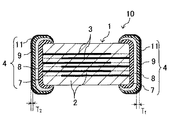
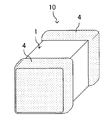
図1は本発明の電子部品を積層セラミックコンデンサに適用した実施形態を示す断面図、図2は図1の積層セラミックコンデンサの外観斜視図であり、図に示す積層セラミックコンデンサ10は、電子部品素体としての積層体1の表面に外部電極4を形成した構造を有している。
FIG. 1 is a sectional view showing an embodiment in which an electronic component of the present invention is applied to a multilayer ceramic capacitor, FIG. 2 is an external perspective view of the multilayer ceramic capacitor of FIG. 1, and the multilayer
前記積層体1は複数個の誘電体層2を間に内部電極3を介して積層することによって形成されており、前記誘電体層2は、例えば、チタン酸バリウム、チタン酸カルシウム、チタン酸ストロンチウム等を主成分とする誘電体材料からなり、その厚みは例えば1μm〜25μmに設定される。また積層体1の内部、具体的には、隣接する誘電体層間2−2に配設される内部電極3は、例えば、Ni、Cu、これらの合金を主成分とする金属材料からなり、その厚みは例えば1μm〜5μmに設定される。
The
尚、上記積層体1を作製するには、先ず、誘電体材料の粉末に適当な有機溶剤、ガラスフリット、有機バインダ等を添加・混合して泥漿状になすとともに、これを従来周知のドクターブレード法等によって所定形状、所定厚みのセラミックグリーンシートを得る。次に、Niの粉末に、ガラスフリットと、有機バインダと溶剤とからなるビヒクルとを混合して得た導体ペーストを、各セラミックグリーンシートの一主面に従来周知のスクリーン印刷法等によって所定パターンに印刷・塗布する。次に、得られたセラミックグリーンシートを従来周知のグリーンシート積層法等にて所定の枚数だけ積層・圧着させることによりセラミックグリーンシートの大型積層体を作製する。この大型積層体を各素子領域毎にダイシング装置を使用して一括的に切断して、未焼成状態の積層体1を形成した。この切断する際、積層体1の対向しあう一対の端面から内部電極3となる導体パターン3の一部が露出するようにしておく。そして、例えば、1100℃〜1400℃の温度で焼成することによって、複数の誘電体層2を間に内部導体3膜を介して積層された直方体状の積層体1が形成される。
In order to manufacture the
また、前記積層体1の表面に形成されている外部電極4は、第1の下地導体層7,第2の下地導体層8、第1メッキ層9、第2メッキ層11を順次、積層した4層構造を有している。
The
第1の下地導体層7は、例えば、Cu、Cu/Niを主成分とする金属材料からなる厚膜導体であり、その厚みは例えば5〜30μmに設定され、積層体1内の内部導体3と電気的に接続される。また、第2の下地導体層8は、例えば、半田耐性を高めるためのものであり、Niメッキ等によって形成され、その厚みは、例えば1μm〜5μmに設定される。
The first
下地導体層7,8を形成するには、先ず、球状Cu/Ni粉末、フレーク状Cu/Ni粉末及びガラス粉末を含む粉末に、有機バインダと溶剤とからなるビヒクルを混合して導体ペーストを製作する。このようにして得られた導体ペーストを、従来周知のディップ法若しくはスクリーン印刷法等によって積層体1の側面に印刷・塗布する。尚、印刷・塗布したときに、ペーストが積層体1の上面、下面及び他の側面に回り込み、第1の下地導体層7の一部を形成している。次に、上記導体ペーストを600℃〜900℃で焼成して積層体1の側面に焼き付けることにより、厚膜導体としての第1の下地導体層7を形成する。このとき、焼き付けられた第1の下地導体層7は、導体ペーストを塗布する前に積層体1の側面に露出させておいた内部電極2の外周部と電気的に接続されることとなる。そして、第1の下地導体層7の表面に、電解メッキ等の湿式メッキ法を用いて表面にNiのメッキ層を形成することにより、第2の下地導体層8が形成される。
To form the
他方、第1メッキ層9は、少なくともSnを含有するメッキ層から成り、その厚みは、例えば3μm以上に設定される。また、第2メッキ層11は、第1メッキ層9よりも表層側に形成されており、その材質としては第1メッキ層9よりも低融点のSn合金、例えば、Sn−Ag、Sn−Cu、Sn−Bi等が用いられ、その厚みは、例えば、0.01μm〜0.05μmに設定される。
On the other hand, the
上記第1メッキ層9及び第2メッキ層11の形成には、先に述べた第2の下地導体層8を形成する場合と同様に、電解メッキ等の湿式メッキが用いられる。
In the formation of the
かくして上述した積層セラミックコンデンサ10は、マザーボード等の外部配線基板上に従来周知の半田付け等によって実装されるようになっており、他の電気回路や電子部品等と共に所定の回路を構成する能動部品として機能することとなる。
Thus, the multilayer
以上のような本実施形態の電子部品は、外部電極4の外層が半田濡れ性の良好な2種類のメッキ層、即ち、Snを含有する第1メッキ層9と、第1メッキ層9よりも低融点のSn合金から成る第2メッキ層11とで構成されている。しかも融点の低い第2メッキ層11が融点の高い第1メッキ層9よりも表層側に配置させてあることから、電子部品を半田付けによって外部配線基板上に実装する際、半田リフロー用の炉の中の温度が第2メッキ層11の融点(半田の固相線温度近く)に達すると、第2メッキ層11を形成するSn合金が半田と馴染んで半田の溶融を促進するとともに、第1メッキ層9の表面を露出させる。このとき、外部電極4の表面状態は露出した第1メッキ層9の融点に支配されているため、半田濡れの加速は有効に抑えられており、半田が外部電極4の表面を伝って這い上がるまでにはならない。その後、炉の中の温度を更に第1メッキ層9の融点付近(半田液相線温度近く)まで上昇させると、第1メッキ層9を形成するSn等が溶融して半田と馴染むため、半田が外部電極4の表面を伝って這いあがろうとするものの、この時点では既に半田が外部配線基板と接合されているため、“チップ立ち現象”を抑止する力が作用するようになっており、このように半田濡れ性の良好な2種類のメッキ層を2段階のタイミングで半田と馴染ませながら半田接合することにより、電子部品を良好かつ安定的に実装することが可能となる。
In the electronic component of the present embodiment as described above, the outer layer of the
また本実施形態の電子部品は、第2メッキ層11の厚みを第1メッキ層9の厚みより薄くすることによって半田の溶融を促進するとともに、第2メッキ層11を第1メッキ層9へ拡散して第2メッキ層11を露出させ、外部電極4側面への半田濡れを抑えるという働きを促進している、特に第2メッキ層11の厚みを0.01μm〜0.05μmに設定することによって、外部電極4側面への半田濡れをより有効におさえることができる。
In the electronic component of this embodiment, the second plating layer 11 is made thinner than the
尚、本発明は上述した実施形態に限定されるものではなく、本発明の要旨を逸脱しない範囲において種々の変更、改良等が可能である。 The present invention is not limited to the above-described embodiments, and various changes and improvements can be made without departing from the scope of the present invention.
例えば上述した実施形態において、第2メッキ層11の表面に、第2メッキ層11よりも更に融点の低いSn合金メッキ層を積層することにより外部電極4を構成するようにしても構わない。
For example, in the above-described embodiment, the
また上述した実施形態では、下地電極層を、厚膜導体から成る第1の下地導体層7とNiメッキ膜から成る第2の下地導体層8とを積層して形成するようにしたが、これに代えて、Niメッキ膜から成る単層の下地導体層によって形成するようにしても構わない。この場合、電子部品素体の表面に露出させた内部電極の露出部に上記下地導体層が直接、接続されることとなる。
In the embodiment described above, the base electrode layer is formed by laminating the first
更に上述した実施形態においては、本発明の電子部品を積層セラミックコンデンサに適用した場合を例にとって説明したが、本発明は、積層セラミックコンデンサ以外の電子部品にも適用可能であることは言うまでもない。
(実験例)
Further, in the above-described embodiment, the case where the electronic component of the present invention is applied to a multilayer ceramic capacitor has been described as an example. However, it is needless to say that the present invention can be applied to electronic components other than the multilayer ceramic capacitor.
(Experimental example)
次に本発明の作用効果を実験例に基づいて説明する。 Next, the effect of this invention is demonstrated based on an experiment example.
まず、第1メッキ層及び第2メッキ層のそれぞれの厚みを変えた積層セラミックコンデンサのサンプルを作製し、半田濡れ評価試験及びチップ立ち性評価試験を行った。作製したサンプルは、第1メッキ層をSnの厚み1〜4μmの範囲で4種類とし、第2メッキ層をSn−Cuの厚み0.005〜1μmの範囲で6種類とした。実験は、半田ペーストを所定位置に印刷した試験用ガラスエポキシ基板に上記積層セラミックコンデンサのサンプルを乗せたものを予熱150℃、120秒、ピーク温度が230度、10秒、のプロファイルのリフロー炉を通過させて行った。半田ペーストとしては、Sn/Ag/Cuの重量比が98.5/1.0/0.5のものを用いた。その試験結果を表1に示す。なお、この実験の評価は、半田濡れ評価試験はサンプルが半田に覆われている面積が90%未満を×、90〜95%を△、95%以上を〇とした。またチップ立ち性評価試験は各々100個のサンプルについてサンプルの片方電極が試験用基板から外れてサンプルが立ち上がっている数をカウントし、発生数が“0”のものを良品とした。
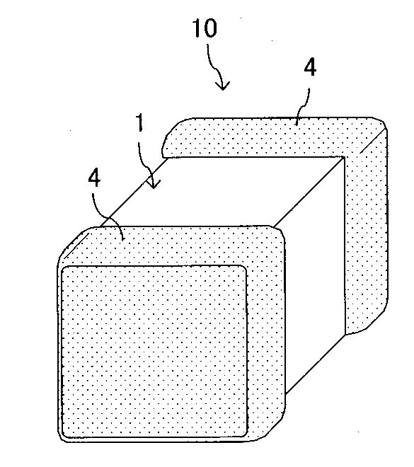
表1によれば、第2メッキ層厚み0.01〜0.05μmにてチップ立ちが発生せず、かつ第1メッキ層厚み3μm以上で半田濡れ性の良いことが確認された。 According to Table 1, it was confirmed that no chip standing occurred when the thickness of the second plating layer was 0.01 to 0.05 μm, and good solder wettability was obtained when the thickness of the first plating layer was 3 μm or more.
またSnにCu、AgまたはBiを配合した材料を使用して既知の合金メッキ法によって第2メッキ層の膜厚0.03μmで融点を変化させた8種類のコンデンササンプルを作成し同じく半田評価試験を行った。その試験結果を表2に示す。
表2によれば、第1メッキ層と第2メッキ層の融点の差が12〜18℃の範囲でチップ立ちが発生しないことが確認された。従って第1メッキ層の融点が第2メッキ層の融点よりも12〜18℃高温にすることが好ましい。 According to Table 2, it was confirmed that no chip standing occurred when the difference in melting point between the first plating layer and the second plating layer was in the range of 12 to 18 ° C. Therefore, it is preferable that the melting point of the first plating layer is 12 to 18 ° C. higher than the melting point of the second plating layer.
1・・・積層体
2・・・誘電体層
3・・・内部電極
4・・・外部電極
7、8・・・下地導体層
9・・・第1メッキ層(Snメッキ層)
10・・・積層セラミックコンデンサ
11・・・第2メッキ層(Sn−Cuメッキ層)
DESCRIPTION OF
10 ... Multilayer ceramic capacitor 11 ... Second plating layer (Sn-Cu plating layer)
Claims (6)
前記外部電極は、下地導体層と、下地導体層上に少なくとも錫を含有する第1メッキ層と、該第1メッキ層よりも低融点の錫合金から成る第2メッキ層とを、前記第2メッキ層が前記第1メッキ層よりも表層側となるように両者を積層して形成されていることを特徴とする電子部品。 In an electronic component having an external electrode soldered to an external electric circuit on the surface of the electronic component body,
The external electrode includes a base conductor layer, a first plating layer containing at least tin on the base conductor layer, and a second plating layer made of a tin alloy having a melting point lower than that of the first plating layer. An electronic component characterized by being formed by laminating both layers so that the plating layer is on the surface layer side of the first plating layer.
Priority Applications (1)
| Application Number | Priority Date | Filing Date | Title |
|---|---|---|---|
| JP2004108879A JP4544896B2 (en) | 2004-04-01 | 2004-04-01 | Electronic components |
Applications Claiming Priority (1)
| Application Number | Priority Date | Filing Date | Title |
|---|---|---|---|
| JP2004108879A JP4544896B2 (en) | 2004-04-01 | 2004-04-01 | Electronic components |
Publications (2)
| Publication Number | Publication Date |
|---|---|
| JP2005294618A true JP2005294618A (en) | 2005-10-20 |
| JP4544896B2 JP4544896B2 (en) | 2010-09-15 |
Family
ID=35327199
Family Applications (1)
| Application Number | Title | Priority Date | Filing Date |
|---|---|---|---|
| JP2004108879A Expired - Fee Related JP4544896B2 (en) | 2004-04-01 | 2004-04-01 | Electronic components |
Country Status (1)
| Country | Link |
|---|---|
| JP (1) | JP4544896B2 (en) |
Cited By (7)
| Publication number | Priority date | Publication date | Assignee | Title |
|---|---|---|---|---|
| JP2013080875A (en) * | 2011-10-05 | 2013-05-02 | Rohm Co Ltd | Electrode structure for electronic component |
| US20140321025A1 (en) * | 2012-01-23 | 2014-10-30 | Murata Manufacturing Co., Ltd. | Electronic component and manufacturing method therefor |
| JPWO2013132966A1 (en) * | 2012-03-05 | 2015-07-30 | 株式会社村田製作所 | Method for forming electronic component and bonded structure of electronic component and object to be bonded |
| JP2016105501A (en) * | 2016-02-03 | 2016-06-09 | ローム株式会社 | Electrode structure for electronic component |
| US9530560B2 (en) | 2013-07-10 | 2016-12-27 | Murata Manufacturing Co., Ltd. | Ceramic electronic component with low equivalent series resistance and method for manufacturing the same |
| US20170069420A1 (en) * | 2014-02-19 | 2017-03-09 | Tdk Corporation | Coil component and terminal component used therein |
| CN112185704A (en) * | 2019-07-04 | 2021-01-05 | 三星电机株式会社 | Multilayer ceramic capacitor |
Citations (6)
| Publication number | Priority date | Publication date | Assignee | Title |
|---|---|---|---|---|
| JPH02296314A (en) * | 1989-05-10 | 1990-12-06 | Matsushita Electric Ind Co Ltd | Manufacture of chip component |
| JP2000280090A (en) * | 1999-01-29 | 2000-10-10 | Fuji Electric Co Ltd | Solder alloy |
| JP2001230151A (en) * | 2000-02-16 | 2001-08-24 | Matsushita Electric Ind Co Ltd | Leadless chip parts |
| JP2001332165A (en) * | 2000-03-16 | 2001-11-30 | Uchihashi Estec Co Ltd | Fuse element and electric component with built-in fuse |
| JP2002359105A (en) * | 2001-05-31 | 2002-12-13 | Tdk Corp | Glass diode type NTC thermistor |
| JP2003163135A (en) * | 2001-11-28 | 2003-06-06 | Nec Tokin Corp | Laminated chip element |
-
2004
- 2004-04-01 JP JP2004108879A patent/JP4544896B2/en not_active Expired - Fee Related
Patent Citations (6)
| Publication number | Priority date | Publication date | Assignee | Title |
|---|---|---|---|---|
| JPH02296314A (en) * | 1989-05-10 | 1990-12-06 | Matsushita Electric Ind Co Ltd | Manufacture of chip component |
| JP2000280090A (en) * | 1999-01-29 | 2000-10-10 | Fuji Electric Co Ltd | Solder alloy |
| JP2001230151A (en) * | 2000-02-16 | 2001-08-24 | Matsushita Electric Ind Co Ltd | Leadless chip parts |
| JP2001332165A (en) * | 2000-03-16 | 2001-11-30 | Uchihashi Estec Co Ltd | Fuse element and electric component with built-in fuse |
| JP2002359105A (en) * | 2001-05-31 | 2002-12-13 | Tdk Corp | Glass diode type NTC thermistor |
| JP2003163135A (en) * | 2001-11-28 | 2003-06-06 | Nec Tokin Corp | Laminated chip element |
Cited By (9)
| Publication number | Priority date | Publication date | Assignee | Title |
|---|---|---|---|---|
| JP2013080875A (en) * | 2011-10-05 | 2013-05-02 | Rohm Co Ltd | Electrode structure for electronic component |
| US20140321025A1 (en) * | 2012-01-23 | 2014-10-30 | Murata Manufacturing Co., Ltd. | Electronic component and manufacturing method therefor |
| US9437365B2 (en) * | 2012-01-23 | 2016-09-06 | Murata Manufacturing Co., Ltd. | Electronic component and manufacturing method therefor |
| JPWO2013132966A1 (en) * | 2012-03-05 | 2015-07-30 | 株式会社村田製作所 | Method for forming electronic component and bonded structure of electronic component and object to be bonded |
| US9530560B2 (en) | 2013-07-10 | 2016-12-27 | Murata Manufacturing Co., Ltd. | Ceramic electronic component with low equivalent series resistance and method for manufacturing the same |
| US20170069420A1 (en) * | 2014-02-19 | 2017-03-09 | Tdk Corporation | Coil component and terminal component used therein |
| US10186368B2 (en) * | 2014-02-19 | 2019-01-22 | Tdk Corporation | Coil component and terminal component used therein |
| JP2016105501A (en) * | 2016-02-03 | 2016-06-09 | ローム株式会社 | Electrode structure for electronic component |
| CN112185704A (en) * | 2019-07-04 | 2021-01-05 | 三星电机株式会社 | Multilayer ceramic capacitor |
Also Published As
| Publication number | Publication date |
|---|---|
| JP4544896B2 (en) | 2010-09-15 |
Similar Documents
| Publication | Publication Date | Title |
|---|---|---|
| JP4957394B2 (en) | Ceramic electronic component and method for manufacturing the same | |
| KR101127870B1 (en) | Ceramic electronic component and method for manufacturing the same | |
| JP5958479B2 (en) | Electronic component mounting structure | |
| US9144166B2 (en) | Electronic component | |
| CN112908692A (en) | Chip-type electronic component | |
| JPH0684687A (en) | Ceramic chip components and chip component mounting structure | |
| JP6919515B2 (en) | Multilayer ceramic capacitors | |
| JP2019004080A (en) | Electronic component, electronic device, and manufacturing method of electronic component | |
| JP2020061468A (en) | Multilayer ceramic electronic component and mounting structure thereof | |
| JP5725678B2 (en) | Multilayer ceramic electronic component, its manufacturing method and its mounting substrate | |
| US9320146B2 (en) | Electronic circuit module component | |
| JP4463045B2 (en) | Ceramic electronic components and capacitors | |
| JP4544896B2 (en) | Electronic components | |
| KR102816972B1 (en) | Multilayer ceramic capacitor and circuit board | |
| WO2023189448A1 (en) | Layered ceramic capacitor, production method for layered ceramic capacitor, and mounting structure for layered ceramic capacitor | |
| JP4715000B2 (en) | Manufacturing method of chip-type electronic component | |
| JPH0737753A (en) | Chip type parts | |
| JP2001155955A (en) | Electronic component equipped having external terminal electrode and mounting electronic article thereof | |
| JPH05243074A (en) | Chip-like electronic parts and method for forming terminal electrode thereof | |
| JP6260169B2 (en) | Ceramic electronic components | |
| JP2006060148A (en) | Ceramic electronic components and capacitors | |
| JP2005340699A (en) | Surface mounting electronic component, packaging structure and method of electronic component | |
| JP6164228B2 (en) | Module and manufacturing method thereof | |
| KR20140013289A (en) | Ceramic electronic component and manufacturing method thereof | |
| US20090230596A1 (en) | Method of manufacturing multi-layered ceramic substrate |
Legal Events
| Date | Code | Title | Description |
|---|---|---|---|
| A621 | Written request for application examination |
Free format text: JAPANESE INTERMEDIATE CODE: A621 Effective date: 20070213 |
|
| A977 | Report on retrieval |
Free format text: JAPANESE INTERMEDIATE CODE: A971007 Effective date: 20091030 |
|
| A131 | Notification of reasons for refusal |
Free format text: JAPANESE INTERMEDIATE CODE: A131 Effective date: 20091109 |
|
| A521 | Written amendment |
Effective date: 20091226 Free format text: JAPANESE INTERMEDIATE CODE: A523 |
|
| TRDD | Decision of grant or rejection written | ||
| A01 | Written decision to grant a patent or to grant a registration (utility model) |
Effective date: 20100601 Free format text: JAPANESE INTERMEDIATE CODE: A01 |
|
| A01 | Written decision to grant a patent or to grant a registration (utility model) |
Free format text: JAPANESE INTERMEDIATE CODE: A01 |
|
| A61 | First payment of annual fees (during grant procedure) |
Free format text: JAPANESE INTERMEDIATE CODE: A61 Effective date: 20100629 |
|
| FPAY | Renewal fee payment (prs date is renewal date of database) |
Free format text: PAYMENT UNTIL: 20130709 Year of fee payment: 3 |
|
| R150 | Certificate of patent (=grant) or registration of utility model |
Free format text: JAPANESE INTERMEDIATE CODE: R150 |
|
| LAPS | Cancellation because of no payment of annual fees |