JP2005294571A - Field effect transistor - Google Patents
Field effect transistor Download PDFInfo
- Publication number
- JP2005294571A JP2005294571A JP2004108140A JP2004108140A JP2005294571A JP 2005294571 A JP2005294571 A JP 2005294571A JP 2004108140 A JP2004108140 A JP 2004108140A JP 2004108140 A JP2004108140 A JP 2004108140A JP 2005294571 A JP2005294571 A JP 2005294571A
- Authority
- JP
- Japan
- Prior art keywords
- electrode
- field effect
- effect transistor
- semiconductor layer
- transistor element
- Prior art date
- Legal status (The legal status is an assumption and is not a legal conclusion. Google has not performed a legal analysis and makes no representation as to the accuracy of the status listed.)
- Pending
Links
Images

Landscapes
- Thin Film Transistor (AREA)
- Electroluminescent Light Sources (AREA)
Abstract
【課題】本発明は、新たな素子構造によってチャネル長を短くして短チャネル化するとともに、実行的電界移動度を向上させた半導体素子を、低コスト製造プロセスで製造することのできるトランジスタ素子を提供することを目的としている。
【課題手段】本発明に係る電界効果型トランジスタ素子は、基板1に、第1電極5、半導体層6、及び、第2電極4が順次積層され、この多層部位の周囲を取り囲むように電気絶縁層3が形成され、該電気絶縁層3の上面に、ゲート電極2が形成されていることを特徴とする。
【選択図】図1
The present invention provides a transistor element capable of manufacturing a semiconductor element having a short channel length by shortening the channel length by a new element structure and improving effective electric field mobility by a low-cost manufacturing process. It is intended to provide.
In a field effect transistor device according to the present invention, a first electrode 5, a semiconductor layer 6, and a second electrode 4 are sequentially stacked on a substrate 1, and are electrically insulated so as to surround the periphery of the multilayer portion. A layer 3 is formed, and a gate electrode 2 is formed on the upper surface of the electrical insulating layer 3.
[Selection] Figure 1
Description
本発明は、電界効果型トランジスタに関し、更に詳しくは、ドレイン電極、半導体層、ソース電極、ゲート絶縁層及びゲート電極が積層され、ゲート電極の電気信号によって電流値を制御する電界効果型トランジスタに関し、特に、シートディスプレイ等のコンピュータ用駆動演算回路として用いられる電界効果型トランジスタに適したものである。 The present invention relates to a field effect transistor, and more particularly to a field effect transistor in which a drain electrode, a semiconductor layer, a source electrode, a gate insulating layer, and a gate electrode are stacked, and a current value is controlled by an electric signal of the gate electrode. In particular, it is suitable for a field effect transistor used as a drive arithmetic circuit for a computer such as a sheet display.
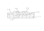
半導体層にアモルファスシリコン(a−Si)或いはポリシリコン(p−Si)を用いた電界効果型トランジスタは、既にアクティブマトリクス型液晶ディスプレイ用、或いは有機EL表示装置用として実用化されている。図4はa−Si或いはp−Siを用いた電界効果型トランジスタの構造の一例である。図4に示す電界効果型トランジスタは基板11に対してソース電極15及びドレイン14が横方向に配置されている。つまり、ソース電極15及びドレイン電極14は、電気的に中性であるシリコン半導体層(チャネル層領域)16により分離されて設けられている。ゲート電極12は、ゲート絶縁層13によりシリコン半導体層16と電気的に分離されて、基板11の上に配置している。
A field effect transistor using amorphous silicon (a-Si) or polysilicon (p-Si) as a semiconductor layer has already been put into practical use for an active matrix liquid crystal display or an organic EL display device. FIG. 4 shows an example of the structure of a field effect transistor using a-Si or p-Si. In the field effect transistor shown in FIG. 4, the source electrode 15 and the
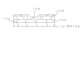
近年、印刷法のような低コスト製造プロセスへの関心の高まりから、半導体層の形成に有機材料を用いた電界効果トランジスタが注目されている。図5及び図6は、有機半導体材料を用いた電界効果トランジスタの素子構造例である。図5に示すように、有機材料を用いた場合でも、前記シリコン材料を用いたトランジスタと同様に、ソース電極105及びドレイン電極104は、ドープしたシリコン基板101に対し横方向に配置されている構造が一般的である。ゲート電極(図示省略)は、ゲート絶縁層103により有機半導体層106と電気的に絶縁されて、基板101の上に配置している。 In recent years, a field effect transistor using an organic material for forming a semiconductor layer has attracted attention due to an increasing interest in a low-cost manufacturing process such as a printing method. 5 and 6 show examples of element structures of field effect transistors using organic semiconductor materials. As shown in FIG. 5, even when an organic material is used, the source electrode 105 and the drain electrode 104 are arranged in a lateral direction with respect to the doped silicon substrate 101 as in the case of the transistor using the silicon material. Is common. A gate electrode (not shown) is electrically insulated from the organic semiconductor layer 106 by the gate insulating layer 103 and disposed on the substrate 101.
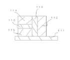
一方、特許文献1所載のトランジスタ構造が存在し、この特許文献1のトランジスタ構造は、図6に示すように、ドレイン電極114、半導体層116、ソース電極115が、基板111上に縦に順次積層されたものである。ここで、ゲート電極112及びゲート絶縁層113は、共に基板111上に形成されており、具体的には、ドレイン電極114、半導体層116及びソース電極115の三層の横方向に隣接してゲート絶縁層113が配置され、該ゲート絶縁層113の横方向に隣接してゲート電極112が配置されている。このような積層型の素子構造を用いることにより、チャネル長を横型素子に比べ短くできるので、有機半導体材料のような比較的高抵抗半導体材料を用いても、充分なドレイン電流が得られる。なお、このような有機半導体層を構成する半導体材料としては、π電子共役系の高分子化合物、芳香族化合物等の有機材料が一般に用いられる。
既述の電界効果トランジスタは、それぞれゲート絶縁層を介してゲート電極より印加された電界が半導体層(チャネル部)に作用して、ソース電極とドレイン電極との間に流れる電流を制御することによりトランジスタ動作を実現している。 In the above-described field effect transistor, the electric field applied from the gate electrode via the gate insulating layer acts on the semiconductor layer (channel portion) to control the current flowing between the source electrode and the drain electrode. Transistor operation is realized.
半導体層に有機材料を用いた電界効果トランジスタは、半導体層にa−Si或いはp−Siを用いた電界効果型トランジスタと比べて、化学気相蒸着法(CVD)のような真空プロセスを必要とせず、印刷法のような簡便なプロセスのみで素子を作製できるため、製造方法が簡便になり、製造コストを低減できるという利点を持っている。しかしながら、半導体層に有機材料を用いた電界効果トランジスタは、半導体層にa−Si或いはp−Siを用いた電界効果型トランジスタと比べて、キャリア移動度が低く、大電流を流すことができない。従って高速動作ができないという問題があった。 A field effect transistor using an organic material for a semiconductor layer requires a vacuum process such as chemical vapor deposition (CVD) as compared with a field effect transistor using a-Si or p-Si for a semiconductor layer. In addition, since the device can be manufactured only by a simple process such as a printing method, there is an advantage that the manufacturing method becomes simple and the manufacturing cost can be reduced. However, a field effect transistor using an organic material for a semiconductor layer has lower carrier mobility and cannot pass a large current compared to a field effect transistor using a-Si or p-Si for a semiconductor layer. Therefore, there is a problem that high-speed operation cannot be performed.
従来、このような問題を解決するために、一つとしては有機材料の改善が試みられている。 Conventionally, in order to solve such problems, one attempt has been made to improve organic materials.
つまり、有機材料面からの改善として、例えば、π共役系高分子の共役状態を制御する技術、分子電気伝導異方性を用いる技術等の分子設計面に関わる技術、及び、蒸着法にて有機高分子膜を得る際に高い結晶性を実現させる技術が提案されている。 In other words, improvements from the organic material side include, for example, techniques related to molecular design such as a technique for controlling the conjugated state of a π-conjugated polymer, a technique using molecular electrical conduction anisotropy, and an organic method by vapor deposition. A technique for realizing high crystallinity when a polymer film is obtained has been proposed.
一方、素子構造の改善により上記問題を解決することも提案されている。つまり、図4及び図5に示される電界効果型トランジスタは、ソース電極とドレイン電極との間に電圧を印加した状態でゲート電極に電圧を印加して、ゲート絶縁層と半導体層との界面にチャネルを誘起させることにより、ソース電極とドレイン電極との間に電流を流すものであるが、このときのソース電極とドレイン電極との間の電流(Id)は、一般に次式で表すことができる。
Id=〔W・Cox・?・?Vg−Vth〕2〕/(2・L) (1)式
なお、数式中におけるCox、?、Vg及びVthは次の通りである。
Cox:ゲート容量(F/m2)
?:キャリア移動度(cm2/Vs)
Vg:ゲート電圧(V)
Vth:しきい値電圧(V)
On the other hand, it has also been proposed to solve the above problem by improving the element structure. That is, the field effect transistor shown in FIGS. 4 and 5 applies a voltage to the gate electrode in a state where a voltage is applied between the source electrode and the drain electrode, and causes the interface between the gate insulating layer and the semiconductor layer. By inducing a channel, a current flows between the source electrode and the drain electrode. At this time, the current (Id) between the source electrode and the drain electrode can be generally expressed by the following equation. .
Id = [W · Cox ·? ·? Vg−Vth] 2 ] / (2 · L) (1) Equation Cox,?, Vg and Vth in the equation are as follows.
Cox: Gate capacity (F / m 2 )
?: Carrier mobility (cm 2 / Vs)
Vg: Gate voltage (V)
Vth: threshold voltage (V)
上記式(1)を参照すると、限られたトランジスタ寸法(L:チャネル長、W:チャネル幅)内でトランジスタ性能を向上させるには、より高いId値を実現させなければならない。また、Id値を向上させるための他の因子(チャネル長Lやチャネル幅W以外の因子)として、Cox、??の増加が考えられる。従来においては比誘電率の高い材料を用いて実効的なCoxを向上させたもの(特許文献2)、π共役系高分子材料の開発により?を向上させたもの(特許文献3)等が提案されているが、これらは材料開発が行われて初めて実現され得る。また、チャネル長Lを減少させることにより高いIdを得るためには、素子構造の改善が課題となる。ここでチャネル長Lは、リソグラフィー加工の限界に依存しており、前記図4及び図5に示される電界効果トランジスタでは、チャネル長Lの値は5〜10?m程度が限界であった。一方、図6のような、積層型の素子構造にすることにより、L値を数百nmレベルまで小さくすることができ、式(1)より、数百倍にもおよぶId値を得られるようになった。しかしながら、有機材料の移動度の平均値が10-3〜10-4(cm2/Vs)(ベストデータ:10-2(cm2/Vs))であり、a−Siの場合0.5〜2(cm2/Vs)、p−Siの場合10〜100(cm2/Vs)であることから、有機材料の移動度はa−Siに比べ数十倍から数百倍小さく、p−Siと比べれば数千倍以上小さくなり、図6のような、縦型素子構造でも、まだ不充分である。
さらに、液晶表示装置においては、前述のようなトランジスタ素子が、前記ソース電極が画素透明電極に接続され、各画素ごとの液晶駆動を行っている。ここで、各画素においては、画素透明電極の占める領域が視認者に視認される透過領域として使用され、ゲート電極やドレイン電極等の存在領域は不透過領域となっている。このため、図4及び図5に示すような横型にソース電極及びドレイン電極が横方向に配置されたトランジスタ素子を用いた場合には液晶表示装置の透過領域の占める割合(開口率)が低くなり、また、特許文献1所載のものにあっても、ドレイン電極114、半導体層116及びソース電極115の三層と、ゲート絶縁層113と、該ゲート絶縁層113とが横方向に配置されているため、開口率が低いという問題を有している。
Further, in the liquid crystal display device, in the transistor element as described above, the source electrode is connected to the pixel transparent electrode, and the liquid crystal is driven for each pixel. Here, in each pixel, the area occupied by the pixel transparent electrode is used as a transmissive area visually recognized by the viewer, and the existing areas such as the gate electrode and the drain electrode are opaque areas. For this reason, when the transistor element in which the source electrode and the drain electrode are arranged in the horizontal direction as shown in FIGS. 4 and 5 is used, the ratio (aperture ratio) of the transmission region of the liquid crystal display device is low. Further, even in the case of the one described in
本発明は、かかる問題を鑑みてなされてものであり、新たな素子構造によってチャネル長を短くして短チャネル化するとともに、実行的電界移動度を向上させた半導体素子を、低コスト製造プロセスで製造することのできるトランジスタ素子を提供することを目的としている。さらには、TFT液晶表示装置等のアクティブマトリクス型ディスプレイに用いた際に、その開口率を高めることのできるトランジスタ素子を提供することを目的ともする。 The present invention has been made in view of such a problem, and a new element structure shortens the channel length to shorten the channel, and at the same time, provides a semiconductor element with improved effective electric field mobility by a low-cost manufacturing process. An object of the present invention is to provide a transistor element that can be manufactured. It is another object of the present invention to provide a transistor element capable of increasing the aperture ratio when used in an active matrix display such as a TFT liquid crystal display device.
本発明は、上記目的を解決すべく、本発明に係る電界効果型トランジスタ素子は、基板に、第1電極、半導体層、及び、第2電極が順次積層され、この多層部位の周囲を取り囲むように電気絶縁層が形成され、該電気絶縁層の上面に、ゲート電極が形成されていることを特徴とする。 In order to solve the above-described object, the field effect transistor device according to the present invention is configured such that a first electrode, a semiconductor layer, and a second electrode are sequentially stacked on a substrate so as to surround the periphery of the multilayer portion. An electrical insulation layer is formed on the upper surface of the electrical insulation layer, and a gate electrode is formed on the upper surface of the electrical insulation layer.
上記構成を採用することにより、有機半導体材料のように電界移動度がa−Si或いはp−Siより低い材料を用いても、TFT液晶表示装置或いは有機EL表示装置を駆動するのに充分なドレイン電流(Id)が得られるようになった。すなわち、第一電極、半導体層、第二電極、ゲート絶縁膜、ゲート電極を基板に順次積層した構造により、チャネル長をナノメーターのオーダーにまで下げることができる。なお、前記絶縁層は、ゲート電極と他の電極とが短絡することを防ぐ範囲に形成されていれば足り、必ずしも多層部位の周囲全面を覆うことは必須ではない。 By adopting the above configuration, a drain sufficient to drive a TFT liquid crystal display device or an organic EL display device even when a material having a field mobility lower than a-Si or p-Si, such as an organic semiconductor material, is used. Current (Id) can be obtained. That is, the channel length can be reduced to the nanometer order by the structure in which the first electrode, the semiconductor layer, the second electrode, the gate insulating film, and the gate electrode are sequentially laminated on the substrate. The insulating layer only needs to be formed in a range that prevents the gate electrode and the other electrode from being short-circuited, and it is not always necessary to cover the entire periphery of the multilayer portion.
また、上記構造により、半導体層のチャネル領域を、半導体層積層方向に沿って左右2箇所に存在するように形成することができ、このため、実行的ドレイン電流を向上させることができる。 In addition, with the above structure, the channel region of the semiconductor layer can be formed so as to exist at two places on the left and right along the semiconductor layer stacking direction, so that the effective drain current can be improved.
また、第一電極、半導体層、第二電極、ゲート絶縁膜、ゲート電極を基板に順次積層した構造であるため、表示装置に用いた場合にあっては、不透過領域を少なくすることができ、十分な開口率を得ることができる。このように表示装置に用いた場合には、第1電極または第2電極の何れか一方が、表面表示装置の画素電極に接続されていることが好ましい。特に、ゲート電極およびゲート絶縁膜にはピンホールが形成され、該ピンホールを介して前記第1電極または第2電極と画素電極とが電気的に接続されている構成を採用することが好ましい。 In addition, since the first electrode, the semiconductor layer, the second electrode, the gate insulating film, and the gate electrode are sequentially stacked on the substrate, the opaque region can be reduced when used in a display device. A sufficient aperture ratio can be obtained. When used in such a display device, it is preferable that either the first electrode or the second electrode is connected to the pixel electrode of the surface display device. In particular, it is preferable to adopt a configuration in which a pin hole is formed in the gate electrode and the gate insulating film, and the first electrode or the second electrode and the pixel electrode are electrically connected through the pin hole.
なお、前記電気絶縁層はゲート絶縁層とすることが可能である。さらに、前記半導体層を、無機材料や、低分子及び高分子有機材料より形成することが可能である。また、前記電気絶縁層を、無機材料や、低分子及び高分子有機材料より形成することも可能である。 The electrical insulating layer can be a gate insulating layer. Furthermore, the semiconductor layer can be formed of an inorganic material, a low molecular weight material, and a high molecular weight organic material. In addition, the electrical insulating layer can be formed of an inorganic material, a low molecular weight material, and a high molecular weight organic material.
また、前記第1電極、第2電極、及び、ドレイン電極は、無機材料や、低分子及び高分子有機材料と適切なドーパンドとなる添加剤より形成することが可能である。なお、各電極は同一の材料から構成されても良いし、異なる材料、つまりは、一つの電極が無機材料で構成され、他の材料が上記低分子及び高分子有機材料と適切なドーパンドとなる添加剤で構成されていることも可能である。 In addition, the first electrode, the second electrode, and the drain electrode can be formed of an inorganic material, a low-molecular or high-molecular organic material, and an additive that becomes an appropriate dopant. Each electrode may be composed of the same material, or different materials, that is, one electrode is composed of an inorganic material, and the other material is an appropriate dopant with the low molecular and high molecular organic materials. It can also consist of additives.
また、第1電極および第2電極は、それぞれ、ソース電極およびドレイン電極から構成することが可能である。 The first electrode and the second electrode can be composed of a source electrode and a drain electrode, respectively.
ここで、前記ソース電極は、従来のCVD法で成膜し、フォトリソグラフィーにより加工して形成する方法と、インクジェット法のような印刷法によって形成する方法がある。ここで、ソース電極は、複数本が平行に基板上に形成することが好ましい。 Here, the source electrode may be formed by a conventional CVD method and processed by photolithography, or a printing method such as an inkjet method. Here, a plurality of source electrodes are preferably formed on the substrate in parallel.
また、前記半導体層は、前記ソース電極と同様にCVD法とフォトリソグラフィーを用いても良いが、印刷法を用いた方が低コストである。ここで、半導体層の厚みは、チャネル長に相当するため、特に目的のチャネル長に応じて、正確な制御が必要となる。ドレイン電流値を大きくするためには、膜圧を小さくする程良いが、あまり小さくし過ぎると、ソース電極とドレイン電極が接触する可能性があるので、注意が必要である。なお、半導体層は、一つのソース電極層に複数積層され、つまり、各画素ごとに該半導体層が設けられることが好ましい。 The semiconductor layer may be formed by CVD and photolithography as in the case of the source electrode, but the printing method is less expensive. Here, since the thickness of the semiconductor layer corresponds to the channel length, accurate control is required particularly in accordance with the target channel length. In order to increase the drain current value, it is better to decrease the film pressure. However, if it is too small, there is a possibility that the source electrode and the drain electrode come into contact with each other. Note that a plurality of semiconductor layers are preferably stacked over one source electrode layer, that is, the semiconductor layers are preferably provided for each pixel.
また、前記ドレイン電極は、前記ソース電極と同様の方法により形成することができる。なお、ドレイン電極は、各半導体層ごとにそれぞれ設けられ、つまり、各画素ごとに該ドレイン電極層が設けられていることが好ましい。また、該ドレイン電極層は、各画素の画素電極(透明電極)に電気的に接続されることが好ましい。 Further, the drain electrode can be formed by the same method as the source electrode. Note that the drain electrode is preferably provided for each semiconductor layer, that is, the drain electrode layer is preferably provided for each pixel. The drain electrode layer is preferably electrically connected to the pixel electrode (transparent electrode) of each pixel.
また、前記ゲート絶縁膜は、CVD法とフォトリソグラフィー法の組み合わせで形成することができるが、印刷法によっても形成することができる。ここで、ゲート絶縁膜は、前記ソース電極、半導体層、及び、ドレイン電極が積層されてなる三層の周囲を取り囲むように形成されている。該ゲート絶縁膜は、前記半導体層及びドレイン電極層と同様に各画素ごとに設けられ、つまり、該ゲート絶縁膜は、ゲート電極層を他の電極層と電気的に接続しないように設けられていることが好ましい。 The gate insulating film can be formed by a combination of a CVD method and a photolithography method, but can also be formed by a printing method. Here, the gate insulating film is formed so as to surround the periphery of the three layers in which the source electrode, the semiconductor layer, and the drain electrode are stacked. The gate insulating film is provided for each pixel similarly to the semiconductor layer and the drain electrode layer, that is, the gate insulating film is provided so as not to electrically connect the gate electrode layer to other electrode layers. Preferably it is.
また、ゲート電極も、CVD法による成膜とフォトリソグラフィーによる加工で形成する方法と、印刷法のような溶液プロセスにより形成する方法との二通りによって形成することができる。また、CVD及びフォトリソグラフィーを用いたプロセスと、溶液プロセスの両方が含まれる工程を用いて、デュアル・サイド・ゲート電界効果型トランジスタを作製してもよい。なお、該ゲート電極は、前記ゲート絶縁膜が存在する位置において、前記ソース電極と平面視交差するように複数形成されることが好ましい。 The gate electrode can also be formed in two ways: a method of forming by CVD method and processing by photolithography, and a method of forming by solution process such as printing method. Alternatively, a dual side gate field effect transistor may be manufactured using a process including both a process using CVD and photolithography and a solution process. Note that a plurality of the gate electrodes are preferably formed so as to intersect the source electrode in a plan view at the position where the gate insulating film exists.
なお、上述しているトランジスタ素子は縦型構造であり、半導体層中に形成されるチャネルは、基板面に対して上下方向である。したがって、半導体層として、芳香族化合物系有機材料のπ電子雲が上下方向に形成される環状化合物を採用すると、かかる環状化合物にとって特に有効な素子構造である Note that the transistor element described above has a vertical structure, and a channel formed in the semiconductor layer is in a vertical direction with respect to the substrate surface. Therefore, when a cyclic compound in which a π electron cloud of an aromatic compound organic material is formed in the vertical direction is adopted as the semiconductor layer, the element structure is particularly effective for the cyclic compound.
また、本発明に係る電界効果型トランジスタ素子の製造方法は、基板に、第1電極、半導体層、及び、第2電極を順次積層し、この三層の周囲を取り囲むように電気絶縁層を形成し、該電気絶縁層の上面に、ゲート電極が形成することを特徴とする。これにより、既述の利点を有する電界効果型トランジスタ素子を製造することができる。 In the method of manufacturing a field effect transistor element according to the present invention, a first electrode, a semiconductor layer, and a second electrode are sequentially stacked on a substrate, and an electric insulating layer is formed so as to surround the three layers. A gate electrode is formed on the upper surface of the electrical insulating layer. Thereby, a field effect transistor element having the above-described advantages can be manufactured.
なお、液晶表示装置等の表示装置の基板に上記電界効果型トランジスタ素子を形成する場合には、前記ゲート電極及び電気絶縁膜にピンホールを形成し、該ピンホールを介して前記第1電極または第二電極と画素電極とを電気的に接続する構成を採用することが好ましい。 In the case where the field effect transistor element is formed on a substrate of a display device such as a liquid crystal display device, a pinhole is formed in the gate electrode and the electric insulating film, and the first electrode or the It is preferable to employ a configuration in which the second electrode and the pixel electrode are electrically connected.
以上のような本発明にあっては、基板に対して垂直方向にチャネル領域が形成される縦型の電界効果型トランジスタであるため、チャネル長が、従来の横型素子に比べてオーダーで小さくなるため、移動度の低い半導体材料を用いても、充分大きいドレイン電流が得られる。また、本発明のデュアル・サイド・ゲート電界効果トランジスタは、半導体層一層中に、二箇所チャネル領域が形成されるため、より効果的にドレイン電流が得られる。また、素子構造が容易であるため、従来の製造技術と精度でもって、トランジスタを製造することができる。 In the present invention as described above, since it is a vertical field effect transistor in which a channel region is formed in a direction perpendicular to the substrate, the channel length is reduced in order as compared with a conventional lateral element. Therefore, even if a semiconductor material with low mobility is used, a sufficiently large drain current can be obtained. In addition, the dual-side gate field effect transistor of the present invention has a two-channel region formed in one layer of the semiconductor layer, so that a drain current can be obtained more effectively. Further, since the element structure is easy, a transistor can be manufactured with the conventional manufacturing technique and accuracy.
以下、本発明を実施する最良の形態について図面に基づいて説明する。
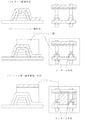
なお、図1は、本発明の一実施の形態の素子構造の模式的断面図を示す。図2は、本発明の一実施の形態の製造工程に関して、CVD法及びフォトリソグラフィー法を用いた場合の様子を説明する図である。図3は、本発明の一実施の形態の製造工程に関して、インクジェット法或いはマイクロコンタクトプリンティング法等の溶液プロセスを用いて製造する工程図である。
The best mode for carrying out the present invention will be described below with reference to the drawings.
FIG. 1 is a schematic cross-sectional view of an element structure according to an embodiment of the present invention. FIG. 2 is a diagram for explaining a state in which a CVD method and a photolithography method are used in the manufacturing process according to the embodiment of the present invention. FIG. 3 is a process diagram of manufacturing using a solution process such as an ink-jet method or a microcontact printing method with respect to the manufacturing process of an embodiment of the present invention.
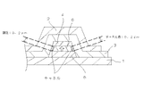
本発明の実施形態のトランジスタ素子は、デュアル・サイド・ゲートトランジスタとして有効に活用されるTFT素子であり、該TFT素子は、図1に示すように、基板上に、ソース電極5(第1電極)、半導体層6(半導体領域)、ドレイン電極(第2電極)、ゲート絶縁膜、及び、ゲート電極2を順次積層してなるものである。
The transistor element of the embodiment of the present invention is a TFT element that is effectively used as a dual side gate transistor, and the TFT element is formed on a substrate with a source electrode 5 (first electrode) as shown in FIG. ), A semiconductor layer 6 (semiconductor region), a drain electrode (second electrode), a gate insulating film, and a
前記ソース電極5は、複数本が平行に同一ピッチで基板1に形成されており、この複数本のソース電極5は、各画素領域の間に配置されている。また、前記ゲート電極層2は、前記ソース電極5と平面視直交するように複数本が平行に同一ピッチで形成されており、この複数本のゲート電極層2も、各画素領域の間に配置されている。そして、前記ソース電極5、半導体層6、ドレイン電極4及びゲート絶縁膜3は、平面視において前記ゲート電極層2と前記ソース電極5とが直交する箇所で、且つ、ゲート電極層2とソース電極5との間に形成されている。
A plurality of the
上記構成からなる本実施形態のTFT素子は、ドレイン電流Idを基板1の面に直交する方向に流し、活性領域(ソース電極5、半導体層6及びドレイン電極4)の周囲に設けられたゲート電極2からゲート絶縁層3を介して半導体層6に電界が印加する構造となっている。ここで、ソース電極5に積層される半導体層6の膜厚Lは薄くすることができるので、従来のようにフォトリソグラフィーの加工精度に依存するものに比して、チャネル長Lを飛躍的に短くした構造を実現できる。その結果、トランジスタ性能、すなわち、実効的なドレイン電流値を向上させることができる。また、半導体素子の構造がシンプルであるので、製造工程を簡略化することができ、そのために、半導体素子の製造コストを低減することができる。
The TFT element of the present embodiment having the above-described configuration allows the drain current Id to flow in a direction orthogonal to the surface of the
また、本実施形態のTFT素子は、前記第一電極(ソース電極5)、半導体層6及び第二電極(ドレイン電極4)の活性領域の周囲にゲート絶縁層3が形成され、更にゲート絶縁層3の周囲に第三電極(ゲート電極2)が設けられている。つまり、半導体層6のチャネル領域が半導体層積層方向に沿って左右2箇所に存在している。このように、半導体層6のチャネル領域は、半導体層6の左右両方に形成されているため、チャネル長Lを短くできる効果に加え、チャネル領域も二箇所形成されるため、より効果的にドレイン電流を流すことができる。
In the TFT element of this embodiment, the
また、平面位置においてソース電極5とゲート電極2とが交差する位置に、前記ソース電極5、半導体層6及びドレイン電極4が配置されることにより、画素電極を大きくとることができ、このため、表示装置の開口率を向上することができる。
Further, the
なお、本発明の半導体素子は、特許文献1で開示されているように、第一電極5と半導体層6との間、又は、半導体層6と第二電極7との間にバッファー層を設けることも適宜設計変更可能な事項である。このようにバッファー層を設けることにより、第一電極5と半導体層6と第二電極7との間に良好な電気的コンタクトを得ることができる。なお、このバッファー層は、例えば、印刷法、インクジェット法等の溶液プロセスで形成可能な導電性高分子材料で形成され、また、ポリチオフェンやポリフェニレン等の他、有機EL用途でよく用いられる低分子系導電性材料を真空蒸着法にて形成してもよい。このように、バッファー層を挿入した素子においては、キャリアは、半導体層とバッファー層の界面に形成された僅かな電位差障壁を越えて伝道するので、特にオフ電流の低減に効果的である。
As disclosed in
前記半導体としては、好ましくは、ナフタレン、アントラセン、テトラセン、ペンタセン、及びそれらの誘導体よりなるアセン分子材料や、フタロシアニン系化合物、アゾ系化合物、ぺリレン系化合物よりなる顔料及びその誘導体や、ヒドラゾン化合物、ジフェニルメタン化合物、トリフェニルメタン化合物、スチルベン化合物、アリールビニル化合物、ピラゾリン化合物、トリフェニルアミン化合物、フェニレン誘導体及びトリアリールアミン化合物よりなる低分子化合物並びにそれらの誘導体や、ポリ−N−ビニルカルバゾール、ポリチオフェン、ポリフェニレン、ポリフェニレンビニレン、ポリアルキルフルオレン、ポリチオナフテン、ポリアニリン、ポリピロール等の高分子化合物等からなる有機半導体材料で構成することができる。このように、半導体を構成する材料が有機半導体材料とすることにより、高分子有機半導体材料を採用した場合には、その溶液をインクジェット法、マイクロコンタクトプリンティング法のような印刷法により成膜することができる。また、低分子有機半導体材料を採用した場合には、これを真空蒸着法等の手段により成膜することができるので、極めて薄い有機半導体層を低コストで形成することができる。 The semiconductor is preferably an acene molecular material composed of naphthalene, anthracene, tetracene, pentacene, and derivatives thereof, a phthalocyanine compound, an azo compound, a pigment composed of a perylene compound and derivatives thereof, a hydrazone compound, Diphenylmethane compounds, triphenylmethane compounds, stilbene compounds, arylvinyl compounds, pyrazoline compounds, triphenylamine compounds, low molecular compounds composed of phenylene derivatives and triarylamine compounds and their derivatives, poly-N-vinylcarbazole, polythiophene, It can be composed of organic semiconductor materials made of polymer compounds such as polyphenylene, polyphenylene vinylene, polyalkylfluorene, polythionaphthene, polyaniline, polypyrrole, etc.In this way, when the material constituting the semiconductor is an organic semiconductor material, when a polymer organic semiconductor material is employed, the solution is formed by a printing method such as an ink jet method or a microcontact printing method. Can do. In addition, when a low molecular organic semiconductor material is employed, it can be formed by means such as vacuum vapor deposition, so that an extremely thin organic semiconductor layer can be formed at low cost.
また、前記半導体層は、a−Si、p−Si等のシリコン、酸化亜鉛、酸化スズ等の金属酸化物のような無機半導体材料で構成されてもかまわない。このように、無機半導体材料を真空蒸着法等の手段により成膜できるので、極めて薄い無機半導体層を製造することができる。 The semiconductor layer may be made of an inorganic semiconductor material such as silicon such as a-Si or p-Si, or metal oxide such as zinc oxide or tin oxide. Thus, since an inorganic semiconductor material can be formed into a film by means such as a vacuum evaporation method, an extremely thin inorganic semiconductor layer can be manufactured.
前記ゲート絶縁層の材料としては、ポリビニルアルコール、ポリビニルブチラール、フェノール樹脂、ノボラック樹脂等のヒドロキシル基を有するポリマー、ポリアクリロニトリル等のシアノ基を有するポリマー、さらには、ポリクロロピレンポリエチレンテレフタレート、ポリオキシメチレン、ポリビニルクロライド、ポリ弗化ビニリデン、ポリメチルメタクリレート、ポリカーボネート、ポリイミド、ポリサルフォン、ポリオルガノシロキサン等のポリマー材料が挙げられる。また、ポリマーだけでなく、SiO2、SiN、Al2O3、等の無機材料を用いても良い。また、ゲート絶縁膜として二層以上の膜を積層することも可能である。また蒸着法やスパッタリング法、塗布法、印刷法またはインクジェット法等材料に応じた公知の成膜方法を用いて膜を堆積した後、フォトリソグラフィー工程及びエッチング工程によって所望の配置のゲート絶縁膜を形成することが可能である。 Examples of the material for the gate insulating layer include polymers having a hydroxyl group such as polyvinyl alcohol, polyvinyl butyral, phenol resin, and novolak resin, polymers having a cyano group such as polyacrylonitrile, polychloropyrene polyethylene terephthalate, polyoxymethylene, Examples thereof include polymer materials such as polyvinyl chloride, polyvinylidene fluoride, polymethyl methacrylate, polycarbonate, polyimide, polysulfone, and polyorganosiloxane. Further, not only polymers but also inorganic materials such as SiO 2 , SiN, Al 2 O 3 may be used. In addition, two or more films can be stacked as the gate insulating film. Also, after depositing a film using a known film formation method according to the material such as a vapor deposition method, a sputtering method, a coating method, a printing method or an ink jet method, a gate insulating film having a desired arrangement is formed by a photolithography process and an etching process. Is possible.
前記第一電極(ソース電極)、第二電極(ドレイン電極)及びゲート電極は、Cr、Al、Ta、Mo、Nb、Cu、Ag、Au、Pt、Pd、In、Ni、Ndおよびこれらの合金や、ポリシリコン、非晶質シリコン、錫酸化物、酸化インジウム、インジウム錫酸化物(ITO;Indium Tin Oxide)等の無機材料や、ドープされた導電性高分子(例えば、ポリエチレンジオキシチオフェン(PEDOT)とポリスチレンスルホン酸ナトリウムとの混合物等)等の有機材料から構成することができる。また二層以上の層から前記電極を形成することも可能である。電極もまた、蒸着法やスパッタリング法、塗布法、印刷法またはインクジェット法等材料に応じた公知の成膜方法を用いて膜を堆積した後、フォトリソグラフィー工程及びエッチング工程によって所望の配置に形成することができる。 The first electrode (source electrode), second electrode (drain electrode), and gate electrode are made of Cr, Al, Ta, Mo, Nb, Cu, Ag, Au, Pt, Pd, In, Ni, Nd, and alloys thereof. And inorganic materials such as polysilicon, amorphous silicon, tin oxide, indium oxide, indium tin oxide (ITO), and doped conductive polymers (eg, polyethylene dioxythiophene (PEDOT)). ) And sodium polystyrene sulfonate, etc.). It is also possible to form the electrode from two or more layers. The electrode is also formed in a desired arrangement by a photolithography process and an etching process after depositing a film using a known film formation method corresponding to a material such as an evaporation method, a sputtering method, a coating method, a printing method, or an ink jet method. be able to.
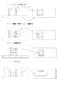
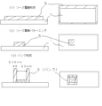
なお、本発明のトランジスタ素子の製造方法の一実施態様を説明すると、まず基板1に第1電極5となる電極膜、半導体層6となる半導体膜及び第2電極4となる電極膜を例えば蒸着法等により順次積層する(図2(1)参照)。そして、エッチング処理により所望の形状の第1電極5、半導体層6及び第2電極4を得る(図2(2)参照)。次に、該第1電極5、半導体層6及び第2電極4の周囲にゲート絶縁膜3を例えば印刷法等により形成する(図2(3)参照)。そして、このゲート絶縁膜3の上面にゲート電極2を、例えば蒸着により成膜した後に、フォトリソグラフィー工程及びエッチング工程によって所望の形状に形成する(図2(4)参照)。
An embodiment of the transistor element manufacturing method of the present invention will be described. First, an electrode film to be the
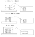
また、本発明のトランジスタ素子の製造方法の他の実施態様を説明すると、まず基板1にレジストからなるバンクを筒状に形成する(図3(1)参照)。そして、この筒状のバンク内に、第1電極5、半導体層6及び第2電極4を順次積層する(図3(2)参照)。次に、第2電極4の上面に、前記バンクと同様の材料によってゲート絶縁膜3を形成する(図3(3)参照)。そして、このゲート絶縁膜3の上面にゲート電極2を形成する(図3(4)参照)。
Further, another embodiment of the transistor element manufacturing method of the present invention will be described. First, a bank made of resist is formed in a cylindrical shape on the substrate 1 (see FIG. 3A). And the
(実施例1)
次に、本発明の具体的な実施例として、以下のデュアル・サイド・ゲートトランジスタをその製造手順とともに図7及び図8を参酌しつつ以下説明する。
(Example 1)
Next, as a specific embodiment of the present invention, the following dual side gate transistor will be described below with reference to FIGS.
まず、本実施例においては、ガラス基板1上にCr層5を膜厚50nmで成膜し(図7(1)参照)、該Cr層5の上面にAu層を膜厚150nmの厚みで成膜する。
First, in this embodiment, a
次に、前記Au膜上にフォトレジストをスピンコートにより塗布し、続いて所定のパターンのマスクを用いて露光、現像する。続いて、Au層及びCr層5を剥離し、最後にNaOH溶液に浸してレジストを剥離し、所望形状のソース電極5を形成する(図7(2)参照)。
Next, a photoresist is applied onto the Au film by spin coating, and then exposed and developed using a mask having a predetermined pattern. Subsequently, the Au layer and the
そして、ソース電極5の全てのサイドに、バンク形成を行った(図7(3)参照)。ここではボラック樹脂を含有するフォトレジストを前記基板1上にスピンコート法により成膜して、このレジスト膜を所望のパターンに露光、現像することにより、前記ソース電極5のサイドにレジストによるゲート絶縁層となるバンク3を形成している。バンク3の幅方向の厚みは200nmとしている。
Then, banks were formed on all sides of the source electrode 5 (see FIG. 7 (3)). Here, a photoresist containing a borak resin is formed on the
次にソース電極5の上部に、インクジェット法により、ポリヘキシルチオフェン膜を作成し、半導体層6を形成する。半導体層6の厚みは200nmになるようにした。また、チャネル幅は20μmとした。さらに、半導体層6の上部に、PEDOT/PSS(ポリエチレンジオキシチオフェン/ポリスチレンスルホン酸塩)による膜をインクジェット法により作成して、ドレイン電極4を形成する(図8(1)参照)。
Next, a polyhexylthiophene film is formed on the
そして、ドレイン電極4の上部に、ドレイン電極4とゲート電極2の接触を避けるための絶縁層として、ノボラック樹脂を含有するフォトレジストをインクジェット法により塗布し、ゲート絶縁層3を形成する(図8(2)参照)。
Then, a photoresist containing a novolac resin is applied on the
ゲート絶縁層の周囲に、ゲート電極2としてTa膜を形成する。Ta膜形成はCVD法とドライエッチング法により形成した(図8(3)参照)。
A Ta film is formed as the
以上の工程で作製したデュアル・サイド・ゲートトランジスタの特性評価を行った。ソース/ドレイン電圧を−20Vから0Vの範囲で変化させ、ゲート電圧を−20Vから0Vの範囲で変化させた。この場合のドレイン電流は150μAだった。ここから既述の式(1)式を用いて得られる移動度は1×10-2cm2/Vsである。またオン/オフ比は106であり、従来のa−Siを用いたトランジスタと同レベルだった。 The characteristics of the dual side gate transistor manufactured through the above steps were evaluated. The source / drain voltage was changed in the range of -20V to 0V, and the gate voltage was changed in the range of -20V to 0V. In this case, the drain current was 150 μA. From here, the mobility obtained by using the above-mentioned formula (1) is 1 × 10 −2 cm 2 / Vs. The on / off ratio was 10 6 , which was the same level as a conventional transistor using a-Si.
(比較例1)
実施例1の比較例として、図6で示される、従来構造のいわゆる横型電界効果型トランジスタの製造に関する比較例1を以下に示す。
高濃度にリンをドープしたSiウエハよりなる基板を1100度で熱酸化処理して、200nmの熱酸化膜を形成する。そして、ソース/ドレイン電極としてAu/Cr膜を積層し、これらの膜にフォトリソグラフィ・エッチングにより、パターンを形成した。チャネル長を5μm、チャネル幅を20μmとした。最後にポリヘキシルチオフェン溶液をスピンコート法により成膜して、横型電界効果トランジスタを作製した。
(Comparative Example 1)
As a comparative example of Example 1, Comparative Example 1 relating to the manufacture of a so-called lateral field effect transistor having a conventional structure shown in FIG.
A substrate made of a Si wafer doped with phosphorus at a high concentration is thermally oxidized at 1100 degrees to form a 200 nm thermal oxide film. Then, Au / Cr films were stacked as source / drain electrodes, and patterns were formed on these films by photolithography etching. The channel length was 5 μm and the channel width was 20 μm. Finally, a polyhexylthiophene solution was formed by spin coating to produce a lateral field effect transistor.
以上の工程で作製した横型電界効果トランジスタの特性評価を行った。ソース/ドレイン電圧を−20Vから0Vの範囲で変化させ、ゲート電圧を−20Vから0Vの範囲で変化させた。この場合のドレイン電流は6μAだった。ここから既述の式(1)を用いて得られる移動度は2×10-2cm2/Vsである。またオン/オフ比は106であり、従来のa−Siを用いたトランジスタと同レベルだった。 The characteristics of the lateral field effect transistor manufactured through the above steps were evaluated. The source / drain voltage was changed in the range of -20V to 0V, and the gate voltage was changed in the range of -20V to 0V. In this case, the drain current was 6 μA. From here, the mobility obtained using the above-described equation (1) is 2 × 10 −2 cm 2 / Vs. The on / off ratio was 10 6 , which was the same level as a conventional transistor using a-Si.
以上の実施例1及び比較例1の結果を比較したところ、キャリア移動度は、同じポリヘキシルチオフェンを用いているにも関わらず、異なった値を示した。これについては、実施例1では、ドレイン電極にPEDOT/PSSを用いており、一方、比較例1では、ソース/ドレイン電極ともAu/Crを用いていること、及び、ゲート絶縁膜に関して実施例1では、有機系高分子材料を用いており、比較例1ではシリコン熱酸化膜を用いているためである。このような要因から、実施例1では、移動度が比較例1に比べて約半分の値であるにも関わらず、ドレイン電流値は、実施例1は、比較例1に比べて25倍ある。一方、オン/オフ比に関して、実施例1と比較例1で違いは見られなかった。 When the results of the above Example 1 and Comparative Example 1 were compared, the carrier mobility showed different values even though the same polyhexylthiophene was used. Regarding this, in Example 1, PEDOT / PSS is used for the drain electrode, while in Comparative Example 1, Au / Cr is used for the source / drain electrode, and for the gate insulating film, Example 1 is used. This is because an organic polymer material is used, and in Comparative Example 1, a silicon thermal oxide film is used. For these reasons, in Example 1, although the mobility is about half that in Comparative Example 1, the drain current value in Example 1 is 25 times that in Comparative Example 1. . On the other hand, no difference was found between Example 1 and Comparative Example 1 with respect to the on / off ratio.
これらの結果より、実施例1のデュアル・サイド・ゲート電界効果トランジスタを用いることにより、移動度の遅い半導体材料を用いても、充分大きいドレイン電流を得ることができ、特に、高分子系有機半導体用素子として有効であることが、確認された。 From these results, by using the dual side gate field effect transistor of Example 1, a sufficiently large drain current can be obtained even when a semiconductor material having a low mobility is used. It was confirmed that it was effective as a device for use.
(実施例2)
次に、本発明の具体的な実施例として、以下のLCDパネルに用いられるTFT素子をその製造手順とともに図9及び図10を参酌しつつ以下説明する。
(Example 2)
Next, as a specific embodiment of the present invention, a TFT element used in the following LCD panel will be described below with reference to FIGS.
まず、実施例2にあっては、基板1上にソース電極5を形成する(図9(1)参照)。ソース電極5はCr及びAuをCVD法により成膜し、フォトリソグラフィー及びドライエッチングにより形成している。ここで、ソース電極5は複数本形成されている。
First, in Example 2, the
次に、半導体層6を、ポリチオフェンをインクジェット法により成膜して形成する(図9(2)参照)。ここでは、半導体層6は、前記ソース電極5の上に複数形成している。
Next, the
そして、前記半導体層6の上面に、ドレイン電極4を形成する(図9(3)参照)。ここで、ソース電極5と同様に、AuをCVD法により成膜し、フォトリソグラフィー及びドライエッチングにより形成した。
Then, the
次に、前記積層された三層の周囲にゲート絶縁膜3を形成する(図9(4)参照)。ここでは、ポリビニルフェノールを用い、インクジェット法により成膜してゲート絶縁膜3を形成した(図8(4)参照)。
Next, a
そして、前記三層の上面を通るようなゲート電極2を形成する(図10(1)参照)。ここでは、AlをCVD法により成膜形成して、前記ゲート電極2を形成した。
Then, a
次に、パッシベーション膜形成を行う。窒化シリコンをCVD法により成膜する(図10(2)参照)。この際、マスク蒸着をおこなうことにより、ドレイン電極上にドレイン電極4まで貫通するピンホールを形成した。
Next, a passivation film is formed. Silicon nitride is formed by a CVD method (see FIG. 10B). At this time, a pin hole penetrating to the
そして、前記パッシベーション膜の上面に、画素電極として、ITO膜を形成する(図10(3)参照)。ここでは、透明電極は、CVD法により成膜し、フォトリソグラフィーおよびウエットエッチングにより形成した。 Then, an ITO film is formed as a pixel electrode on the upper surface of the passivation film (see FIG. 10 (3)). Here, the transparent electrode was formed by a CVD method, and formed by photolithography and wet etching.
1、11、101、111…絶縁性基板、ガラス基板,透明性基板
2、12、102、112…ゲート電極
3、13、103、113…ゲート絶縁層
4、14、104,114…ドレイン電極
5、15、105、115…ソース電極
6、16、106,116…半導体層
DESCRIPTION OF
Claims (12)
この多層部位の周囲を取り囲むように電気絶縁層が形成され、
該電気絶縁層の上面には、ゲート電極が形成されていることを特徴とする
電界効果型トランジスタ素子。 A first electrode, a semiconductor layer, and a second electrode are sequentially stacked on the substrate.
An electrical insulating layer is formed so as to surround the periphery of this multilayer part,
A field effect transistor element, wherein a gate electrode is formed on an upper surface of the electrical insulating layer.
半導体層のチャネル領域が半導体層積層方向に沿って左右2箇所に存在するように形成されていることを特徴とする
電界効果型トランジスタ素子。 The field effect transistor device according to claim 1,
A field effect transistor element, wherein a channel region of a semiconductor layer is formed so as to exist at two places on the left and right along a semiconductor layer stacking direction.
前記第1電極または第2電極の何れか一方が、表面表示装置の画素電極に接続されていることを特徴する
電界効果型トランジスタ素子。 The field effect transistor device according to claim 1 or 2,
Either one of the first electrode or the second electrode is connected to a pixel electrode of a surface display device.
前記電気絶縁層が、ゲート絶縁層であることを特徴する
電界効果型トランジスタ素子。 The field effect transistor device according to any one of claims 1 to 3,
A field effect transistor element, wherein the electrical insulation layer is a gate insulation layer.
前記半導体層が、無機材料より形成されていることを特徴とする
電界効果型トランジスタ素子。 The field effect transistor device according to any one of claims 1 to 4,
A field effect transistor element, wherein the semiconductor layer is made of an inorganic material.
前記半導体層が、低分子及び高分子有機材料より形成されていることを特徴とする
電界効果型トランジスタ素子。 The field effect transistor device according to any one of claims 1 to 4,
A field effect transistor element, wherein the semiconductor layer is formed of a low molecular weight and high molecular organic material.
前記電気絶縁層が、無機材料より形成されていることを特徴とする
電界効果型トランジスタ素子。 The field effect transistor element according to any one of claims 1 to 6,
A field effect transistor element, wherein the electrical insulating layer is made of an inorganic material.
前記電気絶縁層が、低分子及び高分子有機材料より形成されていることを特徴とする
電界効果型トランジスタ素子。 The field effect transistor element according to any one of claims 1 to 6,
A field effect transistor element, wherein the electrical insulating layer is formed of a low molecular weight and high molecular organic material.
前記第1電極、第2電極、及び、ドレイン電極の少なくとも一つが、無機材料より形成されていることを特徴とする
電界効果型トランジスタ素子。 The field effect transistor device according to any one of claims 1 to 8,
A field effect transistor element, wherein at least one of the first electrode, the second electrode, and the drain electrode is formed of an inorganic material.
前記第1電極、第2電極、及び、ドレイン電極の少なくとも一つが、低分子及び高分子有機材料と、適切なドーパンドとなる添加剤より形成されていることを特徴とする
電界効果型トランジスタ素子。 The field effect transistor device according to any one of claims 1 to 8,
A field effect transistor element, wherein at least one of the first electrode, the second electrode, and the drain electrode is formed of a low-molecular and high-molecular organic material and an additive that becomes a suitable dopant.
この三層の周囲を取り囲むように電気絶縁層を形成し、
該電気絶縁層の上面に、ゲート電極が形成することを特徴とする
電界効果型トランジスタ素子の製造方法。 A first electrode, a semiconductor layer, and a second electrode are sequentially stacked on the substrate,
An electrical insulating layer is formed so as to surround the three layers,
A method of manufacturing a field effect transistor element, wherein a gate electrode is formed on an upper surface of the electrical insulating layer.
Priority Applications (1)
| Application Number | Priority Date | Filing Date | Title |
|---|---|---|---|
| JP2004108140A JP2005294571A (en) | 2004-03-31 | 2004-03-31 | Field effect transistor |
Applications Claiming Priority (1)
| Application Number | Priority Date | Filing Date | Title |
|---|---|---|---|
| JP2004108140A JP2005294571A (en) | 2004-03-31 | 2004-03-31 | Field effect transistor |
Publications (1)
| Publication Number | Publication Date |
|---|---|
| JP2005294571A true JP2005294571A (en) | 2005-10-20 |
Family
ID=35327158
Family Applications (1)
| Application Number | Title | Priority Date | Filing Date |
|---|---|---|---|
| JP2004108140A Pending JP2005294571A (en) | 2004-03-31 | 2004-03-31 | Field effect transistor |
Country Status (1)
| Country | Link |
|---|---|
| JP (1) | JP2005294571A (en) |
Cited By (14)
| Publication number | Priority date | Publication date | Assignee | Title |
|---|---|---|---|---|
| WO2007142238A1 (en) * | 2006-06-07 | 2007-12-13 | Panasonic Corporation | Semiconductor element, method for manufacturing the semiconductor element, electronic device and method for manufacturing the electronic device |
| US7932142B2 (en) | 2007-11-14 | 2011-04-26 | Elpida Memory, Inc. | Transistor in a wiring interlayer insulating film |
| WO2011052413A1 (en) * | 2009-10-30 | 2011-05-05 | Semiconductor Energy Laboratory Co., Ltd. | Non-linear element, display device, and electronic device |
| WO2011052410A1 (en) * | 2009-10-30 | 2011-05-05 | Semiconductor Energy Laboratory Co., Ltd. | Power diode, rectifier, and semiconductor device including the same |
| WO2011065209A1 (en) * | 2009-11-27 | 2011-06-03 | Semiconductor Energy Laboratory Co., Ltd. | Non-linear element, display device including non-linear element, and electronic device including display device |
| JP2011119690A (en) * | 2009-10-30 | 2011-06-16 | Semiconductor Energy Lab Co Ltd | Field effect transistor |
| JP2011119691A (en) * | 2009-10-30 | 2011-06-16 | Semiconductor Energy Lab Co Ltd | Field effect transistor |
| JP2011124562A (en) * | 2009-11-13 | 2011-06-23 | Semiconductor Energy Lab Co Ltd | Nonlinear element, display device with the nonlinear element, and electronic apparatus with the display device |
| JP2011129899A (en) * | 2009-11-20 | 2011-06-30 | Semiconductor Energy Lab Co Ltd | Transistor |
| JP2011129898A (en) * | 2009-11-20 | 2011-06-30 | Semiconductor Energy Lab Co Ltd | Transistor |
| US8492806B2 (en) | 2009-10-30 | 2013-07-23 | Semiconductor Energy Laboratory Co., Ltd. | Non-linear element, display device including non-linear element, and electronic device including display device |
| JP2015062248A (en) * | 2009-11-28 | 2015-04-02 | 株式会社半導体エネルギー研究所 | Semiconductor device |
| WO2018203181A1 (en) * | 2017-05-01 | 2018-11-08 | 株式会社半導体エネルギー研究所 | Semiconductor device |
| CN117059626A (en) * | 2023-08-11 | 2023-11-14 | 上海大学 | Thin film transistor and preparation method and application thereof |
-
2004
- 2004-03-31 JP JP2004108140A patent/JP2005294571A/en active Pending
Cited By (47)
| Publication number | Priority date | Publication date | Assignee | Title |
|---|---|---|---|---|
| WO2007142238A1 (en) * | 2006-06-07 | 2007-12-13 | Panasonic Corporation | Semiconductor element, method for manufacturing the semiconductor element, electronic device and method for manufacturing the electronic device |
| US7749921B2 (en) | 2006-06-07 | 2010-07-06 | Panasonic Corporation | Semiconductor element, method for manufacturing the semiconductor element, electronic device and method for manufacturing the electronic device |
| US7932142B2 (en) | 2007-11-14 | 2011-04-26 | Elpida Memory, Inc. | Transistor in a wiring interlayer insulating film |
| JP2015084428A (en) * | 2009-10-30 | 2015-04-30 | 株式会社半導体エネルギー研究所 | Field effect transistor |
| WO2011052410A1 (en) * | 2009-10-30 | 2011-05-05 | Semiconductor Energy Laboratory Co., Ltd. | Power diode, rectifier, and semiconductor device including the same |
| KR101796909B1 (en) * | 2009-10-30 | 2017-12-12 | 가부시키가이샤 한도오따이 에네루기 켄큐쇼 | Non-linear element, display device, and electronic device |
| JP2011119690A (en) * | 2009-10-30 | 2011-06-16 | Semiconductor Energy Lab Co Ltd | Field effect transistor |
| JP2011119691A (en) * | 2009-10-30 | 2011-06-16 | Semiconductor Energy Lab Co Ltd | Field effect transistor |
| JP2017108193A (en) * | 2009-10-30 | 2017-06-15 | 株式会社半導体エネルギー研究所 | Semiconductor device |
| JP2016154254A (en) * | 2009-10-30 | 2016-08-25 | 株式会社半導体エネルギー研究所 | Semiconductor device |
| CN102668095B (en) * | 2009-10-30 | 2016-08-03 | 株式会社半导体能源研究所 | transistor |
| CN102668095A (en) * | 2009-10-30 | 2012-09-12 | 株式会社半导体能源研究所 | transistor |
| US9385114B2 (en) | 2009-10-30 | 2016-07-05 | Semiconductor Energy Laboratory Co., Ltd. | Non-linear element, display device including non-linear element, and electronic device including display device |
| TWI500167B (en) * | 2009-10-30 | 2015-09-11 | Semiconductor Energy Lab | Power diode, rectifier, and semiconductor device including the power diode or the rectifier |
| US8492806B2 (en) | 2009-10-30 | 2013-07-23 | Semiconductor Energy Laboratory Co., Ltd. | Non-linear element, display device including non-linear element, and electronic device including display device |
| US8598635B2 (en) | 2009-10-30 | 2013-12-03 | Semiconductor Energy Laboratory Co., Ltd. | Transistor |
| US8643004B2 (en) | 2009-10-30 | 2014-02-04 | Semiconductor Energy Laboratory Co., Ltd. | Power diode including oxide semiconductor |
| US8704218B2 (en) | 2009-10-30 | 2014-04-22 | Semiconductor Energy Laboratory Co., Ltd. | Semiconductor device having an oxide semiconductor film |
| US8791456B2 (en) | 2009-10-30 | 2014-07-29 | Semiconductor Energy Laboratory Co. Ltd. | Non-linear element, display device including non- linear element, and electronic device including display device |
| US8941107B2 (en) | 2009-10-30 | 2015-01-27 | Semiconductor Energy Laboratory Co., Ltd. | Power diode, rectifier, and semiconductor device including the same |
| US9112041B2 (en) | 2009-10-30 | 2015-08-18 | Semiconductor Energy Laboratory Co., Ltd. | Transistor having an oxide semiconductor film |
| JP2015065466A (en) * | 2009-10-30 | 2015-04-09 | 株式会社半導体エネルギー研究所 | Semiconductor device |
| WO2011052413A1 (en) * | 2009-10-30 | 2011-05-05 | Semiconductor Energy Laboratory Co., Ltd. | Non-linear element, display device, and electronic device |
| US9105609B2 (en) | 2009-10-30 | 2015-08-11 | Semiconductor Energy Laboratory Co., Ltd. | Oxide-based semiconductor non-linear element having gate electrode electrically connected to source or drain electrode |
| TWI496288B (en) * | 2009-10-30 | 2015-08-11 | Semiconductor Energy Lab | Nonlinear component, display device and electronic device |
| JP2015092590A (en) * | 2009-10-30 | 2015-05-14 | 株式会社半導体エネルギー研究所 | Transistor |
| JP2011124562A (en) * | 2009-11-13 | 2011-06-23 | Semiconductor Energy Lab Co Ltd | Nonlinear element, display device with the nonlinear element, and electronic apparatus with the display device |
| JP2015092603A (en) * | 2009-11-20 | 2015-05-14 | 株式会社半導体エネルギー研究所 | Semiconductor device |
| JP2015097275A (en) * | 2009-11-20 | 2015-05-21 | 株式会社半導体エネルギー研究所 | Semiconductor device |
| KR101800852B1 (en) * | 2009-11-20 | 2017-12-20 | 가부시키가이샤 한도오따이 에네루기 켄큐쇼 | Semiconductor device |
| JP2016184767A (en) * | 2009-11-20 | 2016-10-20 | 株式会社半導体エネルギー研究所 | Semiconductor device |
| JP2011129898A (en) * | 2009-11-20 | 2011-06-30 | Semiconductor Energy Lab Co Ltd | Transistor |
| JP2016201562A (en) * | 2009-11-20 | 2016-12-01 | 株式会社半導体エネルギー研究所 | Semiconductor device |
| JP2011129899A (en) * | 2009-11-20 | 2011-06-30 | Semiconductor Energy Lab Co Ltd | Transistor |
| WO2011065209A1 (en) * | 2009-11-27 | 2011-06-03 | Semiconductor Energy Laboratory Co., Ltd. | Non-linear element, display device including non-linear element, and electronic device including display device |
| JP2013062533A (en) * | 2009-11-27 | 2013-04-04 | Semiconductor Energy Lab Co Ltd | Nonlinear element |
| US8390044B2 (en) | 2009-11-27 | 2013-03-05 | Semiconductor Energy Laboratory Co., Ltd. | Non-linear element, display device including non-linear element, and electronic device including display device |
| JP2015097277A (en) * | 2009-11-27 | 2015-05-21 | 株式会社半導体エネルギー研究所 | Semiconductor device |
| US9368640B2 (en) | 2009-11-28 | 2016-06-14 | Semiconductor Energy Laboratory Co., Ltd. | Transistor with stacked oxide semiconductor films |
| JP2015062248A (en) * | 2009-11-28 | 2015-04-02 | 株式会社半導体エネルギー研究所 | Semiconductor device |
| WO2018203181A1 (en) * | 2017-05-01 | 2018-11-08 | 株式会社半導体エネルギー研究所 | Semiconductor device |
| JPWO2018203181A1 (en) * | 2017-05-01 | 2020-03-12 | 株式会社半導体エネルギー研究所 | Semiconductor device |
| JP7128809B2 (en) | 2017-05-01 | 2022-08-31 | 株式会社半導体エネルギー研究所 | semiconductor equipment |
| JP2022159517A (en) * | 2017-05-01 | 2022-10-17 | 株式会社半導体エネルギー研究所 | semiconductor equipment |
| JP7441282B2 (en) | 2017-05-01 | 2024-02-29 | 株式会社半導体エネルギー研究所 | semiconductor equipment |
| JP2024050930A (en) * | 2017-05-01 | 2024-04-10 | 株式会社半導体エネルギー研究所 | Semiconductor Device |
| CN117059626A (en) * | 2023-08-11 | 2023-11-14 | 上海大学 | Thin film transistor and preparation method and application thereof |
Similar Documents
| Publication | Publication Date | Title |
|---|---|---|
| JP5638944B2 (en) | Organic thin film transistor | |
| JP5599190B2 (en) | Method for producing organic thin film transistor | |
| US8089065B2 (en) | Organic thin film transistors | |
| US7919778B2 (en) | Making organic thin film transistor array panels | |
| JP4815765B2 (en) | Method for manufacturing organic semiconductor device | |
| US8963141B2 (en) | Thin-film transistor, fabrication method thereof, and image display device | |
| CN102017209A (en) | Organic thin film transistors | |
| JP2005294571A (en) | Field effect transistor | |
| JP4408903B2 (en) | Transistor, transistor circuit, electro-optical device, and electronic apparatus | |
| US7777220B2 (en) | Organic thin film transistor array panel | |
| CN102017211A (en) | Organic thin film transistor | |
| JP2005167164A (en) | Transistor and manufacturing method thereof | |
| JP5148086B2 (en) | Organic thin film transistor display panel | |
| JP2004111872A (en) | Vertical field-effect transistor, method of manufacturing the same, and arithmetic element having the same | |
| CN108428795B (en) | Thin film transistor, manufacturing method thereof and electronic device including same | |
| KR102277814B1 (en) | Thin film transistor and method of manufacturing the same and electronic device including the thin film transistor | |
| JP2005223049A (en) | Semiconductor device, method for manufacturing semiconductor device, and display device | |
| JP6064353B2 (en) | Thin film transistor manufacturing method | |
| JP5884306B2 (en) | THIN FILM TRANSISTOR, MANUFACTURING METHOD THEREOF, AND ELECTRONIC DEVICE | |
| JP6331644B2 (en) | Thin film transistor array and manufacturing method thereof | |
| JP2016163029A (en) | Thin film transistor, thin film transistor array manufacturing method, and pixel display device | |
| KR101240653B1 (en) | Thin film transistor array panel and method for manufacturing the same | |
| KR101363255B1 (en) | Organic Thin-Film Transistor and Manufacturing Method thereof | |
| JP6123413B2 (en) | Thin film transistor array and image display device | |
| JP5277532B2 (en) | Electronic element |