JP2005294564A - 半導体デバイスおよび半導体デバイスの製造方法 - Google Patents
半導体デバイスおよび半導体デバイスの製造方法 Download PDFInfo
- Publication number
- JP2005294564A JP2005294564A JP2004108050A JP2004108050A JP2005294564A JP 2005294564 A JP2005294564 A JP 2005294564A JP 2004108050 A JP2004108050 A JP 2004108050A JP 2004108050 A JP2004108050 A JP 2004108050A JP 2005294564 A JP2005294564 A JP 2005294564A
- Authority
- JP
- Japan
- Prior art keywords
- film
- interface
- metal
- silicide
- semiconductor device
- Prior art date
- Legal status (The legal status is an assumption and is not a legal conclusion. Google has not performed a legal analysis and makes no representation as to the accuracy of the status listed.)
- Granted
Links
Images

Classifications
-
- H—ELECTRICITY
- H10—SEMICONDUCTOR DEVICES; ELECTRIC SOLID-STATE DEVICES NOT OTHERWISE PROVIDED FOR
- H10D—INORGANIC ELECTRIC SEMICONDUCTOR DEVICES
- H10D64/00—Electrodes of devices having potential barriers
- H10D64/60—Electrodes characterised by their materials
- H10D64/66—Electrodes having a conductor capacitively coupled to a semiconductor by an insulator, e.g. MIS electrodes
- H10D64/68—Electrodes having a conductor capacitively coupled to a semiconductor by an insulator, e.g. MIS electrodes characterised by the insulator, e.g. by the gate insulator
- H10D64/681—Electrodes having a conductor capacitively coupled to a semiconductor by an insulator, e.g. MIS electrodes characterised by the insulator, e.g. by the gate insulator having a compositional variation, e.g. multilayered
- H10D64/685—Electrodes having a conductor capacitively coupled to a semiconductor by an insulator, e.g. MIS electrodes characterised by the insulator, e.g. by the gate insulator having a compositional variation, e.g. multilayered being perpendicular to the channel plane
-
- H—ELECTRICITY
- H01—ELECTRIC ELEMENTS
- H01L—SEMICONDUCTOR DEVICES NOT COVERED BY CLASS H10
- H01L21/00—Processes or apparatus adapted for the manufacture or treatment of semiconductor or solid state devices or of parts thereof
- H01L21/02—Manufacture or treatment of semiconductor devices or of parts thereof
- H01L21/04—Manufacture or treatment of semiconductor devices or of parts thereof the devices having potential barriers, e.g. a PN junction, depletion layer or carrier concentration layer
- H01L21/18—Manufacture or treatment of semiconductor devices or of parts thereof the devices having potential barriers, e.g. a PN junction, depletion layer or carrier concentration layer the devices having semiconductor bodies comprising elements of Group IV of the Periodic Table or AIIIBV compounds with or without impurities, e.g. doping materials
- H01L21/28—Manufacture of electrodes on semiconductor bodies using processes or apparatus not provided for in groups H01L21/20 - H01L21/268
- H01L21/28008—Making conductor-insulator-semiconductor electrodes
- H01L21/28017—Making conductor-insulator-semiconductor electrodes the insulator being formed after the semiconductor body, the semiconductor being silicon
- H01L21/28158—Making the insulator
- H01L21/28167—Making the insulator on single crystalline silicon, e.g. using a liquid, i.e. chemical oxidation
- H01L21/28194—Making the insulator on single crystalline silicon, e.g. using a liquid, i.e. chemical oxidation by deposition, e.g. evaporation, ALD, CVD, sputtering, laser deposition
-
- H—ELECTRICITY
- H10—SEMICONDUCTOR DEVICES; ELECTRIC SOLID-STATE DEVICES NOT OTHERWISE PROVIDED FOR
- H10D—INORGANIC ELECTRIC SEMICONDUCTOR DEVICES
- H10D64/00—Electrodes of devices having potential barriers
- H10D64/60—Electrodes characterised by their materials
- H10D64/66—Electrodes having a conductor capacitively coupled to a semiconductor by an insulator, e.g. MIS electrodes
- H10D64/68—Electrodes having a conductor capacitively coupled to a semiconductor by an insulator, e.g. MIS electrodes characterised by the insulator, e.g. by the gate insulator
- H10D64/691—Electrodes having a conductor capacitively coupled to a semiconductor by an insulator, e.g. MIS electrodes characterised by the insulator, e.g. by the gate insulator comprising metallic compounds, e.g. metal oxides or metal silicates
-
- H—ELECTRICITY
- H01—ELECTRIC ELEMENTS
- H01L—SEMICONDUCTOR DEVICES NOT COVERED BY CLASS H10
- H01L21/00—Processes or apparatus adapted for the manufacture or treatment of semiconductor or solid state devices or of parts thereof
- H01L21/02—Manufacture or treatment of semiconductor devices or of parts thereof
- H01L21/02104—Forming layers
- H01L21/02107—Forming insulating materials on a substrate
- H01L21/02109—Forming insulating materials on a substrate characterised by the type of layer, e.g. type of material, porous/non-porous, pre-cursors, mixtures or laminates
- H01L21/02112—Forming insulating materials on a substrate characterised by the type of layer, e.g. type of material, porous/non-porous, pre-cursors, mixtures or laminates characterised by the material of the layer
- H01L21/02123—Forming insulating materials on a substrate characterised by the type of layer, e.g. type of material, porous/non-porous, pre-cursors, mixtures or laminates characterised by the material of the layer the material containing silicon
- H01L21/02142—Forming insulating materials on a substrate characterised by the type of layer, e.g. type of material, porous/non-porous, pre-cursors, mixtures or laminates characterised by the material of the layer the material containing silicon the material containing silicon and at least one metal element, e.g. metal silicate based insulators or metal silicon oxynitrides
-
- H—ELECTRICITY
- H01—ELECTRIC ELEMENTS
- H01L—SEMICONDUCTOR DEVICES NOT COVERED BY CLASS H10
- H01L21/00—Processes or apparatus adapted for the manufacture or treatment of semiconductor or solid state devices or of parts thereof
- H01L21/02—Manufacture or treatment of semiconductor devices or of parts thereof
- H01L21/02104—Forming layers
- H01L21/02107—Forming insulating materials on a substrate
- H01L21/02109—Forming insulating materials on a substrate characterised by the type of layer, e.g. type of material, porous/non-porous, pre-cursors, mixtures or laminates
- H01L21/022—Forming insulating materials on a substrate characterised by the type of layer, e.g. type of material, porous/non-porous, pre-cursors, mixtures or laminates the layer being a laminate, i.e. composed of sublayers, e.g. stacks of alternating high-k metal oxides
-
- H—ELECTRICITY
- H10—SEMICONDUCTOR DEVICES; ELECTRIC SOLID-STATE DEVICES NOT OTHERWISE PROVIDED FOR
- H10D—INORGANIC ELECTRIC SEMICONDUCTOR DEVICES
- H10D64/00—Electrodes of devices having potential barriers
- H10D64/60—Electrodes characterised by their materials
- H10D64/66—Electrodes having a conductor capacitively coupled to a semiconductor by an insulator, e.g. MIS electrodes
- H10D64/667—Electrodes having a conductor capacitively coupled to a semiconductor by an insulator, e.g. MIS electrodes the conductor comprising a layer of alloy material, compound material or organic material contacting the insulator, e.g. TiN workfunction layers
Landscapes
- Engineering & Computer Science (AREA)
- Condensed Matter Physics & Semiconductors (AREA)
- Manufacturing & Machinery (AREA)
- General Chemical & Material Sciences (AREA)
- Physics & Mathematics (AREA)
- Chemical Kinetics & Catalysis (AREA)
- Chemical & Material Sciences (AREA)
- General Physics & Mathematics (AREA)
- Crystallography & Structural Chemistry (AREA)
- Computer Hardware Design (AREA)
- Microelectronics & Electronic Packaging (AREA)
- Power Engineering (AREA)
- Insulated Gate Type Field-Effect Transistor (AREA)
- Physical Deposition Of Substances That Are Components Of Semiconductor Devices (AREA)
- Formation Of Insulating Films (AREA)
Abstract
Si基板上に高誘電体材料を成膜したとき、界面ダングリングボンドが多量に残留し、表面欠陥密度(Dit)の増大・移動度の低下・界面反応性の増大・低誘電率層の発生といった重大な問題が発生している。更に高誘電体をゲート絶縁膜に使うと、バンドオフセットが十分に取れない場合がある。
【解決手段】
Siを主成分とする半導体基板上に形成した非金属シリサイド薄膜を用いることで、反応性が低く、水素終端よりも安定な構造が得られる。そのため界面荒れが抑えられ、その結果、表面欠陥密度(Dit)の増大・移動度の低下・界面反応性の増大・低誘電率層の発生という問題が抑えられる。
【選択図】 図1
Description
ここで、非金属シリサイド薄膜の形態としては以下の二つが考えられる。
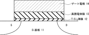
次に、本発明の第1の実施例として、Si基板上にアモルファスHfO2誘電体膜を設けたMOSFETについて説明する。
次に、電極14として、TiNをスパッタ―により成膜した。
このとき、Si基板と誘電体の間の界面欠陥密度Ditを測定すると、およそ9×108cm-2というSi基板上のSiO2薄膜界面の最適化した場合の値を凌駕する良好な値であった。このことは、シリサイド構造を作る過程・その上に高誘電体薄膜を作成する過程を絞り込んだ結果得られたものである。その結果、Si・SiO2界面での電子の移動度以上の高い移動度(550cm2V-1sec-1)が得られており、この界面作成過程が非常に有効であることが確認された。
(第2の実施例)
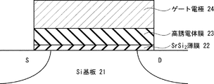
次に、本発明の第2実施例として、Si基板上にアモルファスSrHfO3誘電体膜を設けたMOSFETについて説明する。
すなわち、本実施例のFETは、シリコン基板21の表面部分に、ソース領域S、ドレイン領域Dが形成され、これらの間に形成されたチャネル領域の上に絶縁性シリサイド薄膜22、ゲート絶縁膜23を介してゲート電極24が設けられている。ここで、シリサイドは1ML(Mono Layer)の非金属薄膜SrSi2シリサイドであり、Si基板のダングリングボンドを終端している。
(第三の実施例)
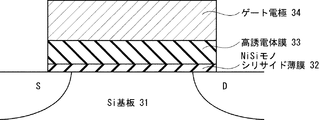
次に、本発明による第3実施例として、Si基板上にアモルファスZrO2誘電体膜を設けたMOSFETについて説明する。
(第4の実施例)
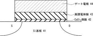
次に、本発明の第4実施例として、Si基板上にエピタキシャルCa(Zr、Ti)O3誘電体膜を設けたMOSFETについて説明する。
すなわち、本実施例のFETは、シリコン基板41の表面部分に、ソース領域S、ドレイン領域Dが形成され、これらの間に形成されたチャネル領域の上に非金属シリサイド薄膜42、ゲート絶縁膜43を介してゲート電極44が設けられている。ここで、シリサイドは1ML(Mono Layer)の非金属シリサイド薄膜CaSi2シリサイドであり、Si基板のダングリングボンドを終端している。
(第5の実施例)
次に、本発明による第5実施例として、Si基板上にアモルファスSrTiO3誘電体膜を設けたMOSFETについて説明する。
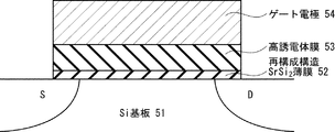
すなわち、本実施例のFETは、シリコン基板51の表面部分に、ソース領域S、ドレイン領域Dが形成され、これらの間に形成されたチャネル領域の上に非金属シリサイド薄膜52、ゲート絶縁膜53を介してゲート電極54が設けられている。ここで、シリサイドは1ML(Mono Layer)の非金属薄膜SrSi2シリサイド上に再構成構造にして4倍の大きさになるようにシリサイド構造を再構成した高抵抗シリサイドであり、Si基板のダングリングボンドを終端している。
(第六の実施例)
次に、本発明による第6実施例として、Si基板上にアモルファスLaAlO3誘電体膜を設けたMOSFETについて説明する。
本発明は、CMOS等のロジック回路や、SRAM、DRAM、フラッシュ、MRAM、FeRAM等のメモリ(特に周辺回路)への適用、さらにはこれらを組み合わせて混載したシステムLSIへの応用も考えられる。
12・・・非金属TiSi2薄膜
13・・・HfO2膜
14・・・TiNゲート電極
22・・・非金属SrSi2薄膜
23・・・SrHfO3高誘電体膜
24、34、44、54、64・・・ゲート電極
32・・・非金属NiSiモノシリサイド薄膜
33・・・ZrO2高誘電体膜
42・・・非金属CaSi2薄膜
43・・・Ca(Ti、Zr)O3高誘電体膜
52・・・非金属SrSi2薄膜
53・・・SrTiO3高誘電体膜
62・・・非金属TiSi薄膜
63・・・LaAlO3高誘電体膜
Claims (14)
- Siを主成分とする半導体基板上に形成された非金属シリサイド薄膜により前記半導体基板のSiのダングリングボンドが終端されていることを特徴とする半導体デバイス。
- 前記非金属シリサイド薄膜は、金属(M)対Siの比が1:2(MSi2)であり、Mは2価もしくは4価の金属であることを特徴とする請求項1記載の半導体デバイス。
- 前記金属(M)は、Mg、Ca、Sr、Ba、Co、Ni、Pd、Pt、Cu、Ag、Zn、 Ti、Zr、Hf、Ce、Mo、W、Ru、Os、Irから選ばれた少なくとも一つの元素であることを特徴とする請求項2記載の半導体デバイス。
- 前記半導体デバイスは、前記非金属シリサイド薄膜上に絶縁膜が形成され、さらにその上に電極が形成されたMIS型電界効果トランジスタであることを特徴とする請求項2記載の半導体デバイス。
- 前記非金属シリサイド薄膜上の絶縁膜は、酸化物、窒化物、酸窒化物の何れかであることを特徴とする請求項4記載の半導体デバイス。
- 前記非金属シリサイド薄膜は、金属(M)対Siの比が1:1(MSi)であり、Mは2価の金属であることを特徴とする請求項1記載の半導体デバイス。
- 前記金属(M)は、Mg、Ca、Sr、Ba、Co、Ni、Pd、Pt、Cu、Ag、Znから選ばれた少なくとも一つの元素であることを特徴とする請求項6記載の半導体デバイス。
- 前記非金属シリサイド薄膜は、金属(M)対Siの比が1:1(MSi)であり、Mは4価の金属であることを特徴とする請求項1記載の半導体デバイス。
- 前記金属(M)は、Ti、Zr、Hf、Ce、Mo、W、Ru、Os、Irから選ばれた少なくとも一つの元素であることを特徴とする請求項8記載の半導体デバイス。
- 前記半導体デバイスは、前記非金属シリサイド薄膜上に絶縁膜が形成され、さらにその上に電極が形成されたMIS型電界効果トランジスタであることを特徴とする請求項6または請求項8記載の半導体デバイス。
- 前記非金属シリサイド薄膜上の絶縁膜は、酸化物、窒化物、酸窒化物の何れかであることを特徴とする請求項10記載の半導体デバイス。
- 前記非金属シリサイドシ薄膜上にさらに高抵抗シリサイド膜が再構成構造を持つように形成されていることを特徴とする請求項1記載の半導体デバイス。
- 請求項1記載の半導体デバイスの非金属シリサイド薄膜を、スパッタ、CVD、ALD、又はMBEのいずれかにより1モノレイヤ形成することを特徴とする半導体デバイスの形成方法。
- 前記非金属シリサイド薄膜上にさらに高抵抗シリサイド膜が再構成構造を持つように形成されていることを特徴とする請求項13に記載の半導体デバイスの形成方法。
Priority Applications (3)
| Application Number | Priority Date | Filing Date | Title |
|---|---|---|---|
| JP2004108050A JP4261408B2 (ja) | 2004-03-31 | 2004-03-31 | 半導体デバイスおよび半導体デバイスの製造方法 |
| US11/049,661 US7115953B2 (en) | 2004-03-31 | 2005-02-04 | Semiconductor device and method of manufacturing semiconductor device |
| CNB2005100524421A CN100492663C (zh) | 2004-03-31 | 2005-02-28 | 半导体器件和半导体器件的制造方法 |
Applications Claiming Priority (1)
| Application Number | Priority Date | Filing Date | Title |
|---|---|---|---|
| JP2004108050A JP4261408B2 (ja) | 2004-03-31 | 2004-03-31 | 半導体デバイスおよび半導体デバイスの製造方法 |
Publications (2)
| Publication Number | Publication Date |
|---|---|
| JP2005294564A true JP2005294564A (ja) | 2005-10-20 |
| JP4261408B2 JP4261408B2 (ja) | 2009-04-30 |
Family
ID=35050091
Family Applications (1)
| Application Number | Title | Priority Date | Filing Date |
|---|---|---|---|
| JP2004108050A Expired - Fee Related JP4261408B2 (ja) | 2004-03-31 | 2004-03-31 | 半導体デバイスおよび半導体デバイスの製造方法 |
Country Status (3)
| Country | Link |
|---|---|
| US (1) | US7115953B2 (ja) |
| JP (1) | JP4261408B2 (ja) |
| CN (1) | CN100492663C (ja) |
Cited By (1)
| Publication number | Priority date | Publication date | Assignee | Title |
|---|---|---|---|---|
| JP2007273531A (ja) * | 2006-03-30 | 2007-10-18 | Toshiba Corp | 半導体装置およびその製造方法 |
Families Citing this family (8)
| Publication number | Priority date | Publication date | Assignee | Title |
|---|---|---|---|---|
| US20060289948A1 (en) * | 2005-06-22 | 2006-12-28 | International Business Machines Corporation | Method to control flatband/threshold voltage in high-k metal gated stacks and structures thereof |
| US7432139B2 (en) * | 2005-06-29 | 2008-10-07 | Amberwave Systems Corp. | Methods for forming dielectrics and metal electrodes |
| US20070001231A1 (en) * | 2005-06-29 | 2007-01-04 | Amberwave Systems Corporation | Material systems for dielectrics and metal electrodes |
| CN103632940B (zh) * | 2012-08-23 | 2016-04-06 | 中芯国际集成电路制造(上海)有限公司 | 一种半导体器件的制造方法 |
| US9496373B2 (en) | 2015-04-02 | 2016-11-15 | International Business Machines Corporation | Damage-resistant fin structures and FinFET CMOS |
| CN107835789B (zh) * | 2015-06-12 | 2020-07-31 | 株式会社丰田自动织机 | 含有CaSi2的组合物及硅材料的制造方法 |
| CN106328509B (zh) * | 2016-08-31 | 2019-05-03 | 上海华力微电子有限公司 | 一种形成mis结构的方法 |
| US20190106805A1 (en) * | 2017-10-10 | 2019-04-11 | Wisconsin Alumni Research Foundation | Crystallization of amorphous multicomponent ionic compounds |
Family Cites Families (1)
| Publication number | Priority date | Publication date | Assignee | Title |
|---|---|---|---|---|
| JP3940552B2 (ja) | 2000-09-25 | 2007-07-04 | 株式会社東芝 | 電界効果トランジスタ及びその製造方法 |
-
2004
- 2004-03-31 JP JP2004108050A patent/JP4261408B2/ja not_active Expired - Fee Related
-
2005
- 2005-02-04 US US11/049,661 patent/US7115953B2/en not_active Expired - Fee Related
- 2005-02-28 CN CNB2005100524421A patent/CN100492663C/zh not_active Expired - Fee Related
Cited By (1)
| Publication number | Priority date | Publication date | Assignee | Title |
|---|---|---|---|---|
| JP2007273531A (ja) * | 2006-03-30 | 2007-10-18 | Toshiba Corp | 半導体装置およびその製造方法 |
Also Published As
| Publication number | Publication date |
|---|---|
| US20050230759A1 (en) | 2005-10-20 |
| CN1677691A (zh) | 2005-10-05 |
| CN100492663C (zh) | 2009-05-27 |
| JP4261408B2 (ja) | 2009-04-30 |
| US7115953B2 (en) | 2006-10-03 |
Similar Documents
| Publication | Publication Date | Title |
|---|---|---|
| US6821873B2 (en) | Anneal sequence for high-κ film property optimization | |
| Wu et al. | High-κ dielectrics and advanced channel concepts for Si MOSFET | |
| TWI278918B (en) | High K dielectric film and method for making | |
| US6852645B2 (en) | High temperature interface layer growth for high-k gate dielectric | |
| US6914312B2 (en) | Field effect transistor having a MIS structure and method of fabricating the same | |
| US7205186B2 (en) | System and method for suppressing oxide formation | |
| TWI512979B (zh) | 含氧阻障層的金屬閘極堆疊的場效電晶體裝置 | |
| US20080293259A1 (en) | METHOD OF FORMING METAL/HIGH-k GATE STACKS WITH HIGH MOBILITY | |
| US8785272B2 (en) | Process to make high-K transistor dielectrics | |
| TW200926293A (en) | Lanthanide dielectric with controlled interfaces | |
| US10068984B2 (en) | Method of manufacturing high-k dielectric using HfO/Ti/Hfo layers | |
| US7601578B2 (en) | Defect control in gate dielectrics | |
| CN106653605B (zh) | 半导体结构的形成方法 | |
| KR100567712B1 (ko) | 반도체 장치 및 이를 제조하기 위한 방법 | |
| US20110037131A1 (en) | Gate structure for field effect transistor | |
| JP4261408B2 (ja) | 半導体デバイスおよび半導体デバイスの製造方法 | |
| JP4309320B2 (ja) | 半導体装置及びその製造方法 | |
| EP2294609B1 (en) | Interfacial layer regrowth control in high-k gate structure for field effect transistor | |
| US7820538B2 (en) | Method of fabricating a MOS device with non-SiO2 gate dielectric | |
| JP2008243994A (ja) | 半導体装置及びその製造方法 | |
| JP2008311661A (ja) | 半導体素子及びそのゲート形成方法 | |
| JP5057957B2 (ja) | 半導体装置及びその製造方法 | |
| JP4757579B2 (ja) | 絶縁ゲート型半導体装置及びその製造方法 | |
| JP2007273587A (ja) | 絶縁膜および半導体装置 | |
| US20160042956A1 (en) | Interface layer for gate stack using 03 post treatment |
Legal Events
| Date | Code | Title | Description |
|---|---|---|---|
| A977 | Report on retrieval |
Free format text: JAPANESE INTERMEDIATE CODE: A971007 Effective date: 20060630 |
|
| A131 | Notification of reasons for refusal |
Free format text: JAPANESE INTERMEDIATE CODE: A131 Effective date: 20080819 |
|
| A131 | Notification of reasons for refusal |
Free format text: JAPANESE INTERMEDIATE CODE: A131 Effective date: 20081114 |
|
| A521 | Request for written amendment filed |
Free format text: JAPANESE INTERMEDIATE CODE: A523 Effective date: 20090113 |
|
| TRDD | Decision of grant or rejection written | ||
| A01 | Written decision to grant a patent or to grant a registration (utility model) |
Free format text: JAPANESE INTERMEDIATE CODE: A01 Effective date: 20090203 |
|
| A01 | Written decision to grant a patent or to grant a registration (utility model) |
Free format text: JAPANESE INTERMEDIATE CODE: A01 |
|
| A61 | First payment of annual fees (during grant procedure) |
Free format text: JAPANESE INTERMEDIATE CODE: A61 Effective date: 20090205 |
|
| FPAY | Renewal fee payment (event date is renewal date of database) |
Free format text: PAYMENT UNTIL: 20120220 Year of fee payment: 3 |
|
| FPAY | Renewal fee payment (event date is renewal date of database) |
Free format text: PAYMENT UNTIL: 20120220 Year of fee payment: 3 |
|
| FPAY | Renewal fee payment (event date is renewal date of database) |
Free format text: PAYMENT UNTIL: 20120220 Year of fee payment: 3 |
|
| FPAY | Renewal fee payment (event date is renewal date of database) |
Free format text: PAYMENT UNTIL: 20130220 Year of fee payment: 4 |
|
| FPAY | Renewal fee payment (event date is renewal date of database) |
Free format text: PAYMENT UNTIL: 20140220 Year of fee payment: 5 |
|
| LAPS | Cancellation because of no payment of annual fees |