JP2005294501A - Electronic circuit unit having connector terminal and circuit board - Google Patents
Electronic circuit unit having connector terminal and circuit board Download PDFInfo
- Publication number
- JP2005294501A JP2005294501A JP2004106890A JP2004106890A JP2005294501A JP 2005294501 A JP2005294501 A JP 2005294501A JP 2004106890 A JP2004106890 A JP 2004106890A JP 2004106890 A JP2004106890 A JP 2004106890A JP 2005294501 A JP2005294501 A JP 2005294501A
- Authority
- JP
- Japan
- Prior art keywords
- circuit board
- noise
- frame ground
- connector terminals
- connector terminal
- Prior art date
- Legal status (The legal status is an assumption and is not a legal conclusion. Google has not performed a legal analysis and makes no representation as to the accuracy of the status listed.)
- Pending
Links
Images
Landscapes
- Shielding Devices Or Components To Electric Or Magnetic Fields (AREA)
- Structure Of Printed Boards (AREA)
Abstract
Description
本発明は、コネクタ端子を有する電子回路ユニットおよびそれに用いられる回路基板に係り、特に、それらのノイズを低減する技術に関する。 The present invention relates to an electronic circuit unit having a connector terminal and a circuit board used for the electronic circuit unit, and more particularly to a technique for reducing such noise.
近年、電子回路基板からの電気的なノイズを低減することが求められている。そのために、電子回路自体にノイズ対策を施した電子回路基板が提案されている。例えば、高周波ノイズを低減するものとして、パワーICにおいて、小信号用の接地とその他の信号用の接地とを区別するという技術が開示されている(特許文献1)。 In recent years, there has been a demand for reducing electrical noise from electronic circuit boards. Therefore, an electronic circuit board has been proposed in which the electronic circuit itself has noise countermeasures. For example, as a technique for reducing high-frequency noise, a technique of distinguishing between small signal grounds and other signal grounds in a power IC is disclosed (Patent Document 1).
また、電子回路部品の動作時に電源層とアース層との間で電圧変動が生じることにより放射されるノイズ低減を図るものとして、電源層として、第1、第2の電源分離パターンと、第1、第2のアース層領域とを設け、第1の電源分離パターンの端部と第1のアース分離パターンとを接続する状態でバイパスコンデンサが、また、第2の電源分離パターンの端部と第2のアース分離パターンとを接続する状態でバイパスコンデンサが設けられ、バイパスコンデンサのそれぞれが、第1、第2電源分離パターンの端部に沿って略一定の間隔で配置されている構造としたものが開示されている(特許文献2)。 In order to reduce noise radiated by voltage fluctuation between the power supply layer and the earth layer during the operation of the electronic circuit component, the power supply layer includes first and second power supply separation patterns, , A second ground layer region is provided, and the bypass capacitor is connected in a state where the end of the first power supply separation pattern and the first ground separation pattern are connected, and the end of the second power supply separation pattern and the second A bypass capacitor is provided in a state where the two earth separation patterns are connected, and each of the bypass capacitors is arranged at substantially constant intervals along the end portions of the first and second power source separation patterns. Is disclosed (Patent Document 2).
さらに、電子装置のケーブルから輻射する不要輻射ノイズを低減するものとして、フレームグランドに接地する接地板にケーブルを固定することによって接地するものが開示されている(特許文献3)。 Furthermore, what reduces the unnecessary radiation noise radiated | emitted from the cable of an electronic device is disclosed by fixing a cable to the ground plate grounded to a frame ground (patent document 3).
ところで、電子機器において問題となるのは、当該機器内部でのノイズの問題に限られない。すなわち、当該電子機器から他の機器に対してノイズを伝えてしまい、他の機器にノイズの影響を与えてしまうという問題がある。この問題が生ずる原因の1つは、コネクタ端子部の共通フレームグランドを介して、ノイズが伝導すること、または、ノイズが放射されることにある。 By the way, what becomes a problem in an electronic device is not limited to the problem of noise inside the device. That is, there is a problem in that noise is transmitted from the electronic device to other devices, and the noise is affected to the other devices. One cause of this problem is that noise is conducted or radiated through the common frame ground of the connector terminal portion.
しかし、従来、この問題についての対策は採られていない。前述した特許文献1では、電子回路基板に搭載される内部回路における設置の問題を扱っている。また、特許文献2では、回路基板における電源層とアース層との間での電圧変動の影響を除去するという問題を扱っている。従って、いずれも、コネクタ端子部の共通フレームグランドを介したノイズを漏洩するための技術を示すものではない。
However, no measures have been taken for this problem.
一方、特許文献3では、ケーブルから輻射するノイズを低減するものである。しかし、ケーブルを接地板に接触させて、フレームグランドに接触させるに過ぎない。これによっても、もちろんある程度のノイズの漏洩を防ぐことができる。 On the other hand, in Patent Document 3, noise radiated from a cable is reduced. However, the cable is merely brought into contact with the ground plate and is brought into contact with the frame ground. This also can prevent a certain amount of noise leakage.
しかし、近年、外部に漏洩する電磁ノイズをできる限り低減することが求められており、この特許文献3の対策では十分ではない。もちろん、ノイズを低減させることは技術的に不可能ではない。しかし、コストをかけずにノイズを低減することは必ずしも容易ではない。 However, in recent years, it has been required to reduce electromagnetic noise leaking to the outside as much as possible, and the countermeasure of Patent Document 3 is not sufficient. Of course, it is not technically impossible to reduce noise. However, it is not always easy to reduce noise without cost.
本発明は、コネクタ端子を介して外部に漏洩されるノイズを低減する技術を提供することを目的とする。 An object of this invention is to provide the technique which reduces the noise leaked outside via a connector terminal.
本発明は、コネクタ端子部のフレームグランドを介して、ノイズが他の信号に、または、他の信号のフレームグランドに伝導することを防止する技術を提供することを目的とする。 It is an object of the present invention to provide a technique for preventing noise from being conducted to other signals or to the frame ground of other signals via the frame ground of the connector terminal portion.
本発明の第1の態様によれば、回路素子群が搭載され、電子機器の筐体に収容される電子回路ユニットにおいて、
前記回路素子群が搭載される回路基板と、
外部との接続を行うための、複数のコネクタ端子と、
前記回路基板に設けられるフレームグランドと、を有し、
前記フレームグランドは、複数の分離領域に分離された状態で、前記回路基板の縁部に沿って配置され、かつ、前記複数の分離領域は、複数のコネクタ端子に対応して、分散して配置されることを特徴とする電子回路ユニットが提供される。
According to the first aspect of the present invention, in the electronic circuit unit in which the circuit element group is mounted and accommodated in the housing of the electronic device,
A circuit board on which the circuit element group is mounted;
Multiple connector terminals for connecting to the outside,
A frame ground provided on the circuit board,
The frame ground is arranged along the edge of the circuit board in a state of being separated into a plurality of separation regions, and the plurality of separation regions are arranged in a distributed manner corresponding to the plurality of connector terminals. An electronic circuit unit is provided.
また、本発明の他の態様によれば、回路素子群およびコネクタ端子を搭載するための回路基板において、
フレームグランドを有し、
前記フレームグランドは、複数の分離領域に分離された状態で、当該回路基板の縁部に沿って配置され、かつ、前記複数の分離領域は、複数のコネクタ端子に対応して、分散して配置されること
を特徴とする回路基板が提供される。
According to another aspect of the present invention, in the circuit board for mounting the circuit element group and the connector terminal,
Have a frame ground,
The frame ground is arranged along the edge of the circuit board in a state of being separated into a plurality of separation regions, and the plurality of separation regions are arranged in a distributed manner corresponding to the plurality of connector terminals. A circuit board is provided.
本発明によれば、コネクタ端子部のフレームグランドを介して、ノイズが他の信号に、または、他の信号のフレームグランドに伝導することを防止することができる。 According to the present invention, it is possible to prevent noise from being conducted to other signals or to the frame ground of other signals via the frame ground of the connector terminal portion.
以下、本発明の実施形態について図面を参照して説明する。 Embodiments of the present invention will be described below with reference to the drawings.
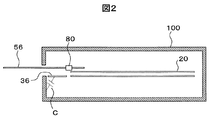
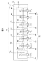
図1は、本発明の第1の実施形態における回路基板の構成を示す平面図である。また、図2に、図1に示す回路基板に他の回路部品等搭載して、電子回路ユニットとして、筐体に収容した状態を示す。 FIG. 1 is a plan view showing a configuration of a circuit board according to the first embodiment of the present invention. FIG. 2 shows a state in which other circuit components are mounted on the circuit board shown in FIG. 1 and are housed in a casing as an electronic circuit unit.
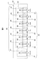
図1に示す本発明の一実施形態に係る回路基板10は、絶縁層11を有し、図2に示す筐体100に収容される。絶縁層11は、例えば、ポリイミド、ガラスエポキシ樹脂等により構成される。一般的には複数層が積層され、各層に、銅等の金属により構成される導体配線が配置される。また、回路基板10には、コネクタ端子群40が設けられる。
A
コネクタ端子群40には、AC入力用の電源用コネクタ端子41、接点出力用コネクタ端子42、ライン用コネクタ端子43、電話用コネクタ端子44、LAN用コネクタ端子46等の複数のコネクタ端子41−47が含まれる。コネクタ端子41には、電源線51が、また、他のコネクタ端子42−47には、それぞれ信号線52−57が接続される。
The
回路基板10には、導体層として、1乃至複数層の電源/グランドパターン20と、フレームグランド30とが、予め定められたパターンにより設けられる。また、この他に、図示していないが、信号伝送のための配線パターンが異なる絶縁層上に設けられる。この回路基板10に、図示していない各種回路素子が搭載され、また、コネクタ端子群40が配置されている。
The
フレームグランド30は、絶縁層11の縁部、すなわち、回路基板10が筐体100に収容された際に、コネクタ端子群30と近接する部分に、コネクタ端子群30の配列に対応して配置される。また、フレームグランド30は、間隙部S1からS6を挟んで、複数の分離領域31−37に分離されて設けられる。本実施形態の場合、コネクタ端子群40を構成する各コネクタ端子41−47に対応して分散配置される。具体的には、一対一対応に設けられる。このフレームグランド30は、電源/グランドパターン20と同様の導体により、同様の製造プロセス、例えば、フォトエッチングプロセス等を経て設けることができる。
The
なお、分離領域31−37の全部または一部については、分離せずに設け、実装時に、導体を切削して間隙部S1からS6を設けることにより、分離するようにしてもよい。また、予め設けた各間隙部S1−S6において、分離領域31−37の隣接する領域について、それぞれ、導電性のフィルム、導体片等の短絡部材により接続して、電気的に一体化しておく。その上で、必要に応じて短絡部材を剥離する等により除去して、間隙部による分離を有効とする構成としてもよい。 Note that all or a part of the separation regions 31-37 may be provided without separation, and may be separated by cutting the conductor to provide the gaps S1 to S6 during mounting. In each of the gap portions S1-S6 provided in advance, the adjacent regions of the separation regions 31-37 are connected by a short-circuit member such as a conductive film or a conductor piece, and are electrically integrated. Then, if necessary, the short-circuit member may be removed by peeling or the like so that the separation by the gap is effective.
各分離領域31−37の大きさは、そもそも、グランドとして機能するために、ある程度の面積が必要である。一方、それらが配置される領域等の事情により、その大きさには制約がある。例えば、それぞれが対応するコネクタ端子41−47の大きさ、コネクタ端子配列密度、間隙部S1−S6の間隔等に応じて大きさが制限される。 The size of each isolation region 31-37 requires a certain area in order to function as a ground in the first place. On the other hand, there are restrictions on the size of the area due to circumstances such as the area in which they are arranged. For example, the size is limited according to the size of the connector terminals 41-47, the density of connector terminals, the spacing between the gap portions S1-S6, and the like.
ここで、間隙部幅、すなわち、間隙部Sを挟む導体間の距離について検討する。間隙部幅は、低減すべきノイズの大きさに応じて定まる。例えば、VCCI(情報処理等電波自主規制協議会)のクラスB規制値では、次のようになる。 Here, the gap width, that is, the distance between conductors sandwiching the gap S will be considered. The gap width is determined according to the magnitude of noise to be reduced. For example, in the class B regulation value of VCCI (Radio Voluntary Regulation Council for Information Processing etc.), it is as follows.
150kHzから30MHzの範囲でのノイズである伝導ノイズについては、
伝導ノイズ:(46dBμV〜67dBμV)
(200μV)〜(2.2mV)
となる。そして、この場合には、間隙部幅、すなわち、分離領域31−37の隣接する領域間の間隔は、2から3mm程度であればよい。
For conduction noise, which is noise in the range of 150 kHz to 30 MHz,
Conduction noise: (46 dBμV to 67 dBμV)
(200 μV) to (2.2 mV)
It becomes. In this case, the gap width, that is, the interval between adjacent regions of the separation regions 31-37 may be about 2 to 3 mm.
また、30MHzから1GHzの範囲での電波ノイズ(放射ノイズ)については、
電波ノイズ:40〜47dBμV/m
(100μV/m)〜(220μV/m)
となる。そして、この場合には、間隙部幅は、1から2mm程度であればよい。
For radio wave noise (radiated noise) in the range of 30 MHz to 1 GHz,
Radio noise: 40 to 47 dBμV / m
(100 μV / m) to (220 μV / m)
It becomes. In this case, the gap width may be about 1 to 2 mm.
一方、間隙部S1−S6のそれぞれの幅は、広いほどノイズの低減性能が向上する。例えば、ノイズレベルが前述した規制値を10%程度超えるような場合、当該部位における間隙部幅を10%広くすることにより、規制値に抑え込めるようにすることができる。 On the other hand, the noise reduction performance is improved as the widths of the gap portions S1 to S6 are increased. For example, when the noise level exceeds the above-mentioned regulation value by about 10%, it is possible to suppress the regulation value to the regulation value by increasing the gap width at the part by 10%.
上述した回路基板は、コネクタ端子群30を取り付け、かつ、図示していない回路素子群を搭載して、筺体100に収容する。図2においては、筺体100を分離領域36において、切断した状態を示す。図2では、コネクタ端子の構造部についての図示は省略して、信号線56のみを示している。
The above-described circuit board is accommodated in the
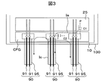
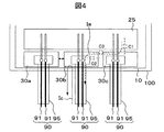
次に、本発明によるノイズ抑止の原理について、図3および図4を参照して説明する。図3に、フレームグランドを共通フレームグランドとした場合を示す。また、図4に、フレームグランドに、本発明を適用して複数の分離領域に分離したものを用いた場合を示す。いずれの場合も、信号グランドのP部に、局所的にノイズ電圧が発生した場合を例として説明する。なお、説明の便宜のため、図1に示す回路基板より簡単な回路構成としてある。
(信号グランドノイズ電流が他の信号線に伝導する場合)
図3に示す共通フレームグランドを用いた回路では、信号グランド25のP部に局所的に発生したノイズ電圧が、ノイズ電流Iaとして、容量C1、C2を通って、信号ケーブル90の信号線91に伝導する。その結果、このノイズ電流に起因して、外部に放射ノイズを発生させ、EMI特性を低下させる。ここで、C1は、信号グランド25と共通フレームグランドCFGとの間の浮遊容量である。また、C2は、共通フレームグランドCFGと信号線91との間の浮遊容量である。
Next, the principle of noise suppression according to the present invention will be described with reference to FIGS. FIG. 3 shows a case where the frame ground is a common frame ground. FIG. 4 shows a case where a frame ground that is separated into a plurality of separation regions by applying the present invention is used. In any case, a case where a noise voltage is locally generated in the P portion of the signal ground will be described as an example. For convenience of explanation, the circuit configuration is simpler than that of the circuit board shown in FIG.
(When signal ground noise current is conducted to other signal lines)
In the circuit using the common frame ground shown in FIG. 3, the noise voltage locally generated at the P portion of the signal ground 25 passes through the capacitors C1 and C2 as the noise current Ia to the
信号グランドのような平板導体の場合、ノイズの平行平板共振によって、強度が局部的大きくなる部分(例えば、P部)が発生する。このようなノイズは、数百メガヘルツと高周波のため、容量C1、C2を通りやすく、外部に伝導しやすい。フレームグランドが共通の場合に、このノイズがすべての信号にのる可能性がある。この場合、ほとんどすべての信号についてフィルタを入れることによって対処することも考えられるが、ノイズ対策が複雑となる。 In the case of a flat conductor such as a signal ground, a portion where the strength is locally increased (for example, a P portion) is generated by parallel plate resonance of noise. Since such noise has a high frequency of several hundred megahertz, it easily passes through the capacitors C1 and C2, and is easily conducted to the outside. If the frame ground is common, this noise can be applied to all signals. In this case, it is conceivable to deal with almost all signals by inserting a filter, but noise countermeasures are complicated.
なお、局部的ノイズとしては、他にLSIの電源電流ノイズ等が考えられる。 In addition, as local noise, LSI power supply current noise and the like can be considered.
これに対して、本発明を適用して、フレームグランドを複数の分離領域30aから30cに分離した場合、図4に示すように、各分離領域30aと30bとの間、30bと30cとの間が、直流的には非導通となる。一方、高周波的にも、浮遊容量C3を小さくすることができることから、ここを通るノイズ電流を小さくすることができる。その結果、ノイズが他の部分に拡散することを防止することができるため、一部の信号についてフィルタを入れるだけで対処することが可能となる。従って、ノイズ対策が非常に簡便なものとなる。
(外部信号のフレームグランドノイズ電流が他の信号のケーブルフレームグランド95または他の信号ラインに伝導する場合)
他の信号のケーブルフレームグランド95または他の信号ラインに伝導したノイズ電流Icは、伝導ノイズまたは放射ノイズとなり、EMI特性を低下させる。フレームグランドが共通の場合、このノイズがすべての信号にのる可能性がある。そのため、すべての信号についてフィルタを入れるなどの対策が必要となる。
On the other hand, when the present invention is applied and the frame ground is separated into a plurality of
(When external signal frame ground noise current is conducted to other signal
The noise current Ic conducted to the
しかし、本発明の場合、フレームグランンドが複数に分離されているため、前述した理由から、ノイズ電流Icがフレームグランド30bから他のフレームグランド(例えば、30a)に流れることがなくなる。そのため、すべてのフレームグランドにノイズがのるという事態になることが避けられる。そのため、一部の信号についてのみノイズ対策をすれば足り、対策が簡便になる。
However, in the case of the present invention, since the frame ground is separated into a plurality, the noise current Ic does not flow from the
なお、以上に述べた本発明が解決しようとする課題は、フレームグランドが筐体に対して浮いている場合でも、また、筐体と接続されている場合でも、同じである。 The problem to be solved by the present invention described above is the same whether the frame ground is floating with respect to the casing or connected to the casing.
次に、本発明の他の実施形態について図5を参照して説明する。図5に示す実施形態は、分離領域の一つである分離領域38を、複数(図5の例では2個)コネクタ端子46、47に対応させたものである。この実施形態の場合でも、前述した実施形態と同様に、間隙部幅を決定することができる。そして、同様の原理により、ノイズ電流の漏洩を低減することができる。
Next, another embodiment of the present invention will be described with reference to FIG. In the embodiment shown in FIG. 5, the
10…回路基板、11…絶縁層、20…電源/グランドパターン、25…信号グランド、30…フレームグランド、31−37…分離領域、40…コネクタ端子群、41−47…コネクタ端子、51…電源線、52−57…信号線、100…筐体。
DESCRIPTION OF
Claims (6)
前記回路素子群が搭載される回路基板と、
外部との接続を行うための、複数のコネクタ端子と、
前記回路基板に設けられるフレームグランドと、を有し、
前記フレームグランドは、複数の分離領域に分離された状態で、前記回路基板の縁部に沿って配置され、かつ、前記複数の分離領域は、複数のコネクタ端子に対応して、分散して配置されること
を特徴とする電子回路ユニット。 In the electronic circuit unit in which the circuit element group is mounted and accommodated in the housing of the electronic device,
A circuit board on which the circuit element group is mounted;
Multiple connector terminals for connecting to the outside,
A frame ground provided on the circuit board,
The frame ground is arranged along the edge of the circuit board in a state of being separated into a plurality of separation regions, and the plurality of separation regions are arranged in a distributed manner corresponding to the plurality of connector terminals. Electronic circuit unit characterized by being made.
前記分離領域は、前記筐体の接地点に対して浮いた状態におかれることを特徴とする電子回路ユニット。 The electronic circuit unit according to claim 1,
The electronic circuit unit according to claim 1, wherein the separation region is placed in a floating state with respect to a grounding point of the casing.
前記分離領域のいずれかは、前記複数のコネクタ端子のうち、2以上のコネクタ端子に対応して配置されることを特徴とする電子回路ユニット。 The electronic circuit unit according to any one of claims 1 and 2,
One of the separation regions is arranged corresponding to two or more connector terminals among the plurality of connector terminals.
フレームグランドを有し、
前記フレームグランドは、複数の分離領域に分離された状態で、当該回路基板の縁部に沿って配置され、かつ、前記複数の分離領域は、複数のコネクタ端子に対応して、分散して配置されること
を特徴とする回路基板。 In circuit boards for mounting circuit element groups and connector terminals,
Have a frame ground,
The frame ground is arranged along the edge of the circuit board in a state of being separated into a plurality of separation regions, and the plurality of separation regions are arranged in a distributed manner corresponding to the plurality of connector terminals. A circuit board characterized by being made.
前記各分離領域は、接地点に対する導通しない状態に形成されることを特徴とする回路基板。 The circuit board according to claim 4,
The circuit board according to claim 1, wherein each of the isolation regions is formed in a non-conductive state with respect to a grounding point.
前記分離領域のいずれかは、前記複数のコネクタ端子のうち、2以上のコネクタ端子に対応して配置されることを特徴とする回路基板。
The circuit board according to any one of claims 4 and 5,
Any of the separation regions is arranged corresponding to two or more connector terminals among the plurality of connector terminals.
Priority Applications (1)
| Application Number | Priority Date | Filing Date | Title |
|---|---|---|---|
| JP2004106890A JP2005294501A (en) | 2004-03-31 | 2004-03-31 | Electronic circuit unit having connector terminal and circuit board |
Applications Claiming Priority (1)
| Application Number | Priority Date | Filing Date | Title |
|---|---|---|---|
| JP2004106890A JP2005294501A (en) | 2004-03-31 | 2004-03-31 | Electronic circuit unit having connector terminal and circuit board |
Publications (1)
| Publication Number | Publication Date |
|---|---|
| JP2005294501A true JP2005294501A (en) | 2005-10-20 |
Family
ID=35327100
Family Applications (1)
| Application Number | Title | Priority Date | Filing Date |
|---|---|---|---|
| JP2004106890A Pending JP2005294501A (en) | 2004-03-31 | 2004-03-31 | Electronic circuit unit having connector terminal and circuit board |
Country Status (1)
| Country | Link |
|---|---|
| JP (1) | JP2005294501A (en) |
Citations (4)
| Publication number | Priority date | Publication date | Assignee | Title |
|---|---|---|---|---|
| JPH0927692A (en) * | 1995-07-12 | 1997-01-28 | Oki Inf Syst | Interface structure |
| JPH11259172A (en) * | 1998-03-06 | 1999-09-24 | Canon Inc | Electronics |
| JP2001148277A (en) * | 1999-11-22 | 2001-05-29 | Sharp Corp | Power supply circuit with lightning surge voltage absorption circuit |
| JP2003283177A (en) * | 2002-03-27 | 2003-10-03 | Yaskawa Electric Corp | Radiation noise reduction device for electronic devices |
-
2004
- 2004-03-31 JP JP2004106890A patent/JP2005294501A/en active Pending
Patent Citations (4)
| Publication number | Priority date | Publication date | Assignee | Title |
|---|---|---|---|---|
| JPH0927692A (en) * | 1995-07-12 | 1997-01-28 | Oki Inf Syst | Interface structure |
| JPH11259172A (en) * | 1998-03-06 | 1999-09-24 | Canon Inc | Electronics |
| JP2001148277A (en) * | 1999-11-22 | 2001-05-29 | Sharp Corp | Power supply circuit with lightning surge voltage absorption circuit |
| JP2003283177A (en) * | 2002-03-27 | 2003-10-03 | Yaskawa Electric Corp | Radiation noise reduction device for electronic devices |
Similar Documents
| Publication | Publication Date | Title |
|---|---|---|
| US5488540A (en) | Printed circuit board for reducing noise | |
| CA2146139C (en) | Electromagnetic radiation reduction technique using grounded conductive traces circumscribing internal planes of printed circuit boards | |
| KR101999509B1 (en) | Circuit board | |
| JP2000286587A (en) | Electromagnetic shield structure of connector for external cable connection | |
| JP5147501B2 (en) | In-vehicle electronic device | |
| KR20200014231A (en) | Circuit board and electronic device including the same | |
| WO2012039120A4 (en) | Printed circuit board | |
| JP6843312B1 (en) | Circuit boards and electronic devices | |
| US7939766B2 (en) | Apparatus for electromagentically shielding a portion of a circuit board | |
| JP2005294511A (en) | Electronic circuit unit having connector terminal and circuit board | |
| JPH09232014A (en) | Interface cable connecting connector | |
| US8208271B2 (en) | Printed board and image formation apparatus | |
| JP5320801B2 (en) | Electronic device and noise shielding method thereof | |
| JP2005294501A (en) | Electronic circuit unit having connector terminal and circuit board | |
| JP2005294502A (en) | Electronic circuit unit having connector terminal and circuit board | |
| KR100512738B1 (en) | Printed circuit board and electronic machine using thereof | |
| JP2008172280A (en) | Electronic circuit unit having connector terminal and circuit board | |
| JP3678658B2 (en) | Power cable connector for EMI countermeasures | |
| JPH11284291A (en) | Circuit board and liquid crystal display device with the circuit board mounted | |
| US20130265675A1 (en) | Digital protective relay | |
| JPH0515317B2 (en) | ||
| JP2006261470A (en) | Multilayer printed circuit board | |
| JP5398888B2 (en) | Electronics | |
| JP5183390B2 (en) | Electronics | |
| JP2001326468A (en) | Multilayer printed wiring boards and electronic equipment |
Legal Events
| Date | Code | Title | Description |
|---|---|---|---|
| A977 | Report on retrieval |
Free format text: JAPANESE INTERMEDIATE CODE: A971007 Effective date: 20060922 |
|
| A131 | Notification of reasons for refusal |
Free format text: JAPANESE INTERMEDIATE CODE: A131 Effective date: 20061003 |
|
| A02 | Decision of refusal |
Free format text: JAPANESE INTERMEDIATE CODE: A02 Effective date: 20070213 |