JP2005294511A - Electronic circuit unit having connector terminal and circuit board - Google Patents
Electronic circuit unit having connector terminal and circuit board Download PDFInfo
- Publication number
- JP2005294511A JP2005294511A JP2004107073A JP2004107073A JP2005294511A JP 2005294511 A JP2005294511 A JP 2005294511A JP 2004107073 A JP2004107073 A JP 2004107073A JP 2004107073 A JP2004107073 A JP 2004107073A JP 2005294511 A JP2005294511 A JP 2005294511A
- Authority
- JP
- Japan
- Prior art keywords
- circuit
- circuit board
- noise
- frame ground
- connector terminals
- Prior art date
- Legal status (The legal status is an assumption and is not a legal conclusion. Google has not performed a legal analysis and makes no representation as to the accuracy of the status listed.)
- Pending
Links
- 238000000926 separation method Methods 0.000 claims description 50
- 239000003990 capacitor Substances 0.000 claims description 27
- 238000002955 isolation Methods 0.000 claims description 19
- 239000000758 substrate Substances 0.000 claims description 5
- 239000002184 metal Substances 0.000 description 9
- 229910052751 metal Inorganic materials 0.000 description 9
- 239000004020 conductor Substances 0.000 description 6
- 238000000034 method Methods 0.000 description 6
- 230000033228 biological regulation Effects 0.000 description 5
- 238000010586 diagram Methods 0.000 description 5
- 239000010408 film Substances 0.000 description 5
- 230000005855 radiation Effects 0.000 description 3
- 230000003068 static effect Effects 0.000 description 3
- 230000005611 electricity Effects 0.000 description 2
- 229910000906 Bronze Inorganic materials 0.000 description 1
- RYGMFSIKBFXOCR-UHFFFAOYSA-N Copper Chemical compound [Cu] RYGMFSIKBFXOCR-UHFFFAOYSA-N 0.000 description 1
- OAICVXFJPJFONN-UHFFFAOYSA-N Phosphorus Chemical compound [P] OAICVXFJPJFONN-UHFFFAOYSA-N 0.000 description 1
- 239000004642 Polyimide Substances 0.000 description 1
- 239000010974 bronze Substances 0.000 description 1
- 239000000919 ceramic Substances 0.000 description 1
- 239000011248 coating agent Substances 0.000 description 1
- 238000000576 coating method Methods 0.000 description 1
- 229910052802 copper Inorganic materials 0.000 description 1
- 239000010949 copper Substances 0.000 description 1
- KUNSUQLRTQLHQQ-UHFFFAOYSA-N copper tin Chemical compound [Cu].[Sn] KUNSUQLRTQLHQQ-UHFFFAOYSA-N 0.000 description 1
- 238000007599 discharging Methods 0.000 description 1
- 239000003822 epoxy resin Substances 0.000 description 1
- 230000002349 favourable effect Effects 0.000 description 1
- 239000011888 foil Substances 0.000 description 1
- 239000011521 glass Substances 0.000 description 1
- 230000005283 ground state Effects 0.000 description 1
- 230000010365 information processing Effects 0.000 description 1
- 238000009434 installation Methods 0.000 description 1
- 239000011810 insulating material Substances 0.000 description 1
- 239000012212 insulator Substances 0.000 description 1
- 238000004519 manufacturing process Methods 0.000 description 1
- 239000000463 material Substances 0.000 description 1
- 239000007769 metal material Substances 0.000 description 1
- 238000001259 photo etching Methods 0.000 description 1
- 229920000647 polyepoxide Polymers 0.000 description 1
- 229920001721 polyimide Polymers 0.000 description 1
- 230000008054 signal transmission Effects 0.000 description 1
- 230000001629 suppression Effects 0.000 description 1
- 239000010409 thin film Substances 0.000 description 1
- 230000002747 voluntary effect Effects 0.000 description 1
Images

Landscapes
- Shielding Devices Or Components To Electric Or Magnetic Fields (AREA)
- Structure Of Printed Boards (AREA)
Abstract
Description
本発明は、コネクタ端子を有する電子回路ユニットおよびそれに用いられる回路基板に係り、特に、それらのノイズを低減する技術に関する。 The present invention relates to an electronic circuit unit having a connector terminal and a circuit board used for the electronic circuit unit, and more particularly to a technique for reducing such noise.
近年、電子回路基板からの電気的なノイズを低減することが求められている。そのために、電子回路自体にノイズ対策を施した電子回路基板が提案されている。例えば、高周波ノイズを低減するものとして、パワーICにおいて、小信号用の接地とその他の信号用の接地とを区別するという技術が開示されている(特許文献1)。 In recent years, there has been a demand for reducing electrical noise from electronic circuit boards. Therefore, an electronic circuit board has been proposed in which the electronic circuit itself has noise countermeasures. For example, as a technique for reducing high-frequency noise, a technique of distinguishing between small signal grounds and other signal grounds in a power IC is disclosed (Patent Document 1).
また、電子回路部品の動作時に電源層とアース層との間で電圧変動が生じることにより放射されるノイズ低減を図るものとして、電源層として、第1、第2の電源分離パターンと、第1、第2のアース層領域とを設け、第1の電源分離パターンの端部と第1のアース分離パターンとを接続する状態でバイパスコンデンサが、また、第2の電源分離パターンの端部と第2のアース分離パターンとを接続する状態でバイパスコンデンサが設けられ、バイパスコンデンサのそれぞれが、第1、第2電源分離パターンの端部に沿って略一定の間隔で配置されている構造としたものが開示されている(特許文献2)。 In order to reduce noise radiated by voltage fluctuation between the power supply layer and the earth layer during the operation of the electronic circuit component, the power supply layer includes first and second power supply separation patterns, , A second ground layer region is provided, and the bypass capacitor is connected in a state where the end of the first power supply separation pattern and the first ground separation pattern are connected, and the end of the second power supply separation pattern and the second A bypass capacitor is provided in a state where the two earth separation patterns are connected, and each of the bypass capacitors is arranged at substantially constant intervals along the end portions of the first and second power source separation patterns. Is disclosed (Patent Document 2).
さらに、電子装置のケーブルから輻射する不要輻射ノイズを低減するものとして、フレームグランドに接地する接地板にケーブルを固定することによって接地するものが開示されている(特許文献3)。 Furthermore, what reduces the unnecessary radiation noise radiated | emitted from the cable of an electronic device is disclosed by fixing a cable to the ground plate grounded to a frame ground (patent document 3).
ところで、電子機器において問題となるのは、当該機器内部でのノイズの問題に限られない。すなわち、当該電子機器から他の機器に対してノイズを伝えてしまい、他の機器にノイズの影響を与えてしまうという問題がある。この問題が生ずる原因の1つは、コネクタ端子を介して、ノイズが伝導すること、または、ノイズが放射されることにある。 By the way, what becomes a problem in an electronic device is not limited to the problem of noise inside the device. That is, there is a problem in that noise is transmitted from the electronic device to other devices, and the noise is affected to the other devices. One cause of this problem is that noise is conducted or radiated through the connector terminals.
しかし、従来、この問題についての対策は採られていない。前述した特許文献1では、電子回路基板に搭載される内部回路における設置の問題を扱っている。また、特許文献2では、回路基板における電源層とアース層との間での電圧変動の影響を除去するという問題を扱っている。従って、いずれも、コネクタ端子を介したノイズを漏洩するための技術を示すものではない。
However, no measures have been taken for this problem.
一方、特許文献3では、ケーブルから輻射するノイズを低減するものである。しかし、ケーブルを接地板に接触させて、フレームグランドに接触させるに過ぎない。これによっても、もちろんある程度のノイズの漏洩を防ぐことができる。
On the other hand, in
しかし、近年、外部に漏洩する電磁ノイズをできる限り低減することが求められており、この特許文献3の対策では十分ではない。もちろん、ノイズを低減させることは技術的に不可能ではない。しかし、コストをかけずにノイズを低減することは必ずしも容易ではない。
However, in recent years, it has been required to reduce electromagnetic noise leaking to the outside as much as possible, and the countermeasure of
本発明は、コネクタ端子部のフレームグランドを介して、ノイズが他の信号に、または、他の信号のフレームグランドに伝導することを防止する技術を提供することを目的とする。 It is an object of the present invention to provide a technique for preventing noise from being conducted to other signals or to the frame ground of other signals via the frame ground of the connector terminal portion.
本発明の第1の態様によれば、回路素子群が搭載され、電子機器の筐体に収容される電子回路ユニットにおいて、
前記回路素子群が搭載される回路基板と、
外部との接続を行うための、複数のコネクタ端子と、
前記回路基板に設けられるフレームグランドと、を有し、
前記フレームグランドは、複数の分離領域に分離された状態で、前記回路基板の縁部に沿って配置され、かつ、前記複数の分離領域は、複数のコネクタ端子に対応して、分散して配置され、
前記分離領域のうち少なくとも一部については、制限回路を介して接地されること
を特徴とする電子回路ユニットが提供される。
According to the first aspect of the present invention, in the electronic circuit unit in which the circuit element group is mounted and accommodated in the housing of the electronic device,
A circuit board on which the circuit element group is mounted;
Multiple connector terminals for connecting to the outside,
A frame ground provided on the circuit board,
The frame ground is arranged along the edge of the circuit board in a state of being separated into a plurality of separation regions, and the plurality of separation regions are arranged in a distributed manner corresponding to the plurality of connector terminals. And
An electronic circuit unit is provided in which at least a part of the separation region is grounded through a limiting circuit.
また、本発明の他の態様によれば、回路素子群およびコネクタ端子を搭載するための回路基板において、
フレームグランドを有し、
前記フレームグランドは、複数の分離領域に分離された状態で、当該回路基板の縁部に沿って配置され、かつ、前記複数の分離領域は、複数のコネクタ端子に対応して、分散して配置され、
前記分離領域のうち少なくとも一部については、制限回路を介して接地されること
を特徴とする回路基板が提供される。
According to another aspect of the present invention, in the circuit board for mounting the circuit element group and the connector terminal,
Have a frame ground,
The frame ground is arranged along the edge of the circuit board in a state of being separated into a plurality of separation regions, and the plurality of separation regions are arranged in a distributed manner corresponding to the plurality of connector terminals. And
A circuit board is provided in which at least a part of the isolation region is grounded through a limiting circuit.
本発明によれば、コネクタ端子部のフレームグランドを介して、ノイズが他の信号に、または、他の信号のフレームグランドに伝導することを防止することができる。 According to the present invention, it is possible to prevent noise from being conducted to other signals or to the frame ground of other signals via the frame ground of the connector terminal portion.
以下、本発明の実施形態について図面を参照して説明する。 Embodiments of the present invention will be described below with reference to the drawings.
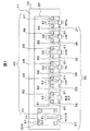
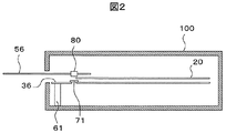
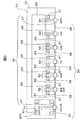
図1は、本発明の第1の実施形態における回路基板の構成を示す平面図である。また、図2に、図1に示す回路基板に他の回路部品等搭載して、電子回路ユニットとして、筐体に収容した状態を示す。 FIG. 1 is a plan view showing a configuration of a circuit board according to the first embodiment of the present invention. FIG. 2 shows a state in which other circuit components are mounted on the circuit board shown in FIG. 1 and are housed in a casing as an electronic circuit unit.
図1に示す本発明の一実施形態に係る回路基板10は、絶縁層11を有し、図2に示す筐体100に収容される。絶縁層11は、例えば、ポリイミド、ガラスエポキシ樹脂等により構成される。一般的には複数層が積層され、各層に、銅等の金属により構成される導体配線が配置される。また、回路基板10には、コネクタ端子群40が設けられる。
A
コネクタ端子群40には、AC入力用の電源用コネクタ端子41、接点出力用コネクタ端子42、ライン用コネクタ端子43、電話用コネクタ端子44、LAN用コネクタ端子46等の複数のコネクタ端子41−47が含まれる。コネクタ端子41には、電源線51が、また、他のコネクタ端子42−47には、それぞれ信号線52−57が接続される。
The
回路基板10には、導体層として、1乃至複数層の電源/グランドパターン20と、フレームグランド30とが、予め定められたパターンで設けられる。また、この他に、図示していないが、信号伝送のための配線パターンが異なる絶縁層上に設けられる。この回路基板10に、図示していない各種回路素子が搭載され、また、コネクタ端子群40が配置されている。
The
フレームグランド30は、絶縁層11の縁部、すなわち、回路基板10が筐体100に収容された際に、コネクタ端子群30と近接する部分に、コネクタ端子群30の配列に対応して配置される。また、フレームグランド30は、スリットS1からS6を挟んで、複数の分離領域31−37に分離されて設けられる。本実施形態の場合、コネクタ端子群40を構成する各コネクタ端子41−47に対応して分散配置される。具体的には、一対一対応に設けられる。このフレームグランド30は、電源/グランドパターン20と同様の導体により、同様の製造プロセス、例えば、フォトエッチングプロセス等を経て設けることができる。また、金属等の導電性の箔を貼り付けることにより構成することもできる。
The
なお、分離領域31−37の全部または一部については、分離せずに設け、実装時に、スリットS1からS6を設けて分離するようにしてもよい。また、予め設けた各スリットS1−S6において、分離領域31−37の隣接する領域について、それぞれ、導電性のフィルム、導体片等の短絡部材により接続して、電気的に一体化しておく。その上で、必要に応じて短絡部材を剥離する等により除去して、スリットによる分離を有効とする構成としてもよい。 Note that all or part of the separation regions 31-37 may be provided without being separated, and may be separated by providing slits S1 to S6 during mounting. In each of the slits S1-S6 provided in advance, the adjacent regions of the separation regions 31-37 are connected by a short-circuit member such as a conductive film or a conductor piece, and are electrically integrated. Then, if necessary, the short-circuit member may be removed by peeling or the like so that the separation by the slit is effective.
各分離領域31−37の大きさは、そもそも、グランドとして機能するために、ある程度の面積が必要である。一方、それらが配置される領域等の事情により、その大きさには制約がある。例えば、それぞれが対応するコネクタ端子41−47の大きさ、コネクタ端子配列密度、スリットS1−S6の間隔等に応じて大きさが制限される。 The size of each isolation region 31-37 requires a certain area in order to function as a ground in the first place. On the other hand, there are restrictions on the size of the area due to circumstances such as the area in which they are arranged. For example, the size is limited according to the size of the connector terminals 41-47, the connector terminal array density, the spacing between the slits S1-S6, etc., respectively.
各分離領域31−37は、それぞれ、制限回路71と、対応する接地部材61とを介して行われる。そのため、各分離領域31−37は、それぞれ対応する接地部材61とは導通しないよう分離されて配置される。なお、図1では、分離領域31については、回路基板20の上面側に制限回路71を接続パッド204と共に設け、他の分離領域32−37については回路基板20の下面側に、接続パッド202と共に設ける構造となっている。これは、分離領域31の面積が広く、他の分離領域32−37の面積が狭いことに基づいて、制限回路71の実装が容易に行えるように考慮したものである。ただし、本発明は、この態様に限定されるものではない。例えば、抵抗体、コンデンサ等の個別部品を、リード線を介して接続する構成とすることもできる。
Each separation region 31-37 is performed via a
制限回路71は、接地を安定に行うために設けられる。例えば、抵抗、コンデンサ、抵抗−コンデンサ直列接続回路、および、抵抗−コンデンサ並列接続回路のいずれかを回路素子として有するものが用いられる。また、制限回路71は、回路素子が素子基板上に形成されたものとすることができる。その一例を、図9(A)および(B)に示す。これらの図に示す例は、例えば、セラミック等の絶縁物により構成される素子基板701上に、抵抗素子702が形成され、さらに、その両端に対向電極703,704が形成されている。抵抗素子702は、薄膜、厚膜等により形成することができる。
The limiting
抵抗を用いる場合には、例えば、数キロΩから数メガΩの範囲のものが用いられる。このように、抵抗を介在させることにより、それが接続された分離領域における電位の安定を図ることができると共に、静電気を放電することにより、帯電を防止することができる。 When a resistor is used, for example, a resistor in the range of several kilo Ω to several mega Ω is used. In this way, by interposing a resistor, it is possible to stabilize the potential in the isolation region to which it is connected, and to prevent static charging by discharging static electricity.
図9に示す例では、抵抗素子のみが設けられている。しかし、この抵抗素子に代えて、または、抵抗素子と直列に、若しくは、並列に、コンデンサを配置することもできる。 In the example shown in FIG. 9, only the resistance element is provided. However, a capacitor may be arranged instead of this resistive element, or in series or in parallel with the resistive element.
コンデンサを用いる場合には、例えば、数十pFから数十μFの範囲のものが用いられる。このように、コンデンサを介在させることにより、低周波ノイズを遮断することができる。 When a capacitor is used, for example, a capacitor in the range of several tens of pF to several tens of μF is used. Thus, low frequency noise can be blocked by interposing a capacitor.
コンデンサと抵抗とを直列に接続した抵抗−コンデンサ直列接続回路は、例えば、数Ωから数十Ωの抵抗と、数十pF以上のコンデンサとの直列接続回路が用いられる。このように、抵抗−コンデンサ直列接続回路を介在させることにより、当該回路の周波数特性に応じて、低周波ノイズの遮断、中周波ノイズの低減、および、高周波ノイズの通過を図ることができる。 As a resistor-capacitor series connection circuit in which a capacitor and a resistor are connected in series, for example, a series connection circuit of a resistor of several Ω to several tens of Ω and a capacitor of several tens of pF or more is used. Thus, by interposing the resistor-capacitor series connection circuit, it is possible to cut off the low frequency noise, reduce the medium frequency noise, and pass the high frequency noise according to the frequency characteristics of the circuit.
また、コンデンサと抵抗とを並列に接続した抵抗−コンデンサ並列接続回路は、例えば、数キロΩから数メガΩの範囲の抵抗と、数十pFから数十μFの範囲のコンデンサとが用いられる。このように、抵抗−コンデンサ並列接続回路を介在させることにより、分離領域における電位の安定を図ることができると共に、静電気を放電すること、直流を遮断すること、および、低周波ノイズを遮断することができる。 In addition, a resistor-capacitor parallel connection circuit in which a capacitor and a resistor are connected in parallel uses, for example, a resistor in the range of several kiloΩ to several megaΩ and a capacitor in the range of several tens of pF to several tens of μF. Thus, by interposing the resistor-capacitor parallel connection circuit, it is possible to stabilize the potential in the isolation region, to discharge static electricity, to block direct current, and to block low-frequency noise. Can do.
分離領域の接地は、具体的な態様としては、導電性を有する連結部材、圧接部材等を接地部材として用いて、各分離領域31−37と筐体100(筐体100と電気的に等価な接地点を含む)とを制限回路71を介して連結することにより行う。連結部材および圧接部材としては、各分離領域31−37と筐体100とを制限回路71を介して電気的に接続できる導電性を有するものであればよい。連結部材は、回路基板10を筐体100に物理的に固定された状態で接地を行う。逆に、各分離領域31−37と筐体100とを制限回路71を介して接地する機能と、回路基板10を筐体100に物理的に固定する機能とを併有する構造とすることができる。ただし、物理的固定手段が他にある場合には、物理的に固定する機能を有しないものであってもよい。圧接部材は、弾性を有する部材を有し、弾性を有する部材を、付勢された状態で、回路基板10と筐体100との間に介在させて、回路基板10と筐体100とに密接した状態で接地を行う。連結部材および圧接部材については後述する。
Specifically, the grounding of the separation region is performed by using each of the separation regions 31-37 and the housing 100 (electrically equivalent to the housing 100) using a conductive connecting member, a pressure contact member, or the like as a grounding member. (Including a grounding point) by connecting via a limiting
なお、本実施形態の場合、各分離領域31−37について制限回路71を介して接地する構造としているが、本発明は、これに限られない。一部の分離領域については、接地部材を介して直接的に接地する構造とすることができる。すなわち、その電子回路ユニットの特性、ノイズ環境等に応じて最適な接地状態とすることができる。
In the present embodiment, each isolation region 31-37 is grounded via the limiting
各分離領域31−37に接続される制限回路71は、同一の特性のものに限られない。分離領域毎に異なる回路構成のもの、抵抗値等の回路パラメータが異なるものを選択して接続し、最適な特性を実現することができる。例えば、回路基板10を筐体100に組み込んで、性能を確認する際に、各分離領域について、制限回路71を接続したり、外したり、さらに、接続を外して短絡したりすることを行って、最適な接地状態を実現することができる。また、介在させるべき制限回路71として、回路構成の異なるもの、さらに、抵抗値、キャパシタンス等の値が異なるもの等を複数種用意しておき、ノイズが最も低減されるものを選択して接続する構成とすることができる。このような構成とすることにより、ノイズ低減を効果的に行うことができる。また、同一仕様の電子回路ユニットについて、各分離領域31−37について、接続すべき制限回路71(浮かせる場合、短絡させる場合を含む)を予め決定しておくことにより、ノイズ低減対策を、量産ラインにおいて効率よく行うことができる。
The limiting
また、介在させるべき制限回路71を着脱可能に接続する構成とすることにより、電子回路ユニットの接地現場において、制限回路71を他の回路構成、他の回路パラメータのものと差し替えること、制限回路を外して、浮かせること、または、短絡することが、必要に応じて適宜行える。これにより、電子回路ユニットについて、それが接地される現場において、そのノイズ環境に合わせて最適化な接地状態とすることができる。ノイズは、現場の環境に応じて種々の発生態様となるため、標準的な設計のみでは対応しにくい場合もある。従って、現場での調整を可能としておくことにより、その場のノイズ環境に適したノイズ低減が容易に行い得る。
Further, by providing a configuration in which the limiting
分離領域31においては、接地部材61は、図1に示すように、分離領域31の面積を考慮して、分離領域の四隅に1個ずつ設けている。一方、分離領域32−37においては、対応する接地部材61は、図1に示すように、分離領域32−37のそれぞれに2箇所ずつ設けられている。なお、これは、例示であり、配置される位置および個数は、これに限られない。
In the
次に、スリット幅について検討する。スリット幅は、低減すべきノイズの大きさに応じて定まる。例えば、VCCI(情報処理等電波自主規制協議会)のクラスB規制値では、次のようになる。 Next, the slit width will be examined. The slit width is determined according to the magnitude of noise to be reduced. For example, in the class B regulation value of VCCI (Radio Voluntary Regulation Council for Information Processing etc.), it is as follows.
150kHzから30MHzの範囲でのノイズである伝導ノイズについては、
伝導ノイズ:(46dBμV〜67dBμV)
(200μV)〜(2.2mV)
となる。そして、この場合には、スリット幅、すなわち、分離領域31−37の隣接する領域間の間隔は、2から3mm程度であればよい。
For conduction noise, which is noise in the range of 150 kHz to 30 MHz,
Conduction noise: (46 dBμV to 67 dBμV)
(200 μV) to (2.2 mV)
It becomes. In this case, the slit width, that is, the interval between adjacent regions of the separation regions 31-37 may be about 2 to 3 mm.
また、30MHzから1GHzの範囲での電波ノイズ(放射ノイズ)については、
電波ノイズ:40〜47dBμV/m
(100μV/m)〜(220μV/m)
となる。そして、この場合には、スリット幅は、1から2mm程度であればよい。
For radio wave noise (radiated noise) in the range of 30 MHz to 1 GHz,
Radio noise: 40 to 47 dBμV / m
(100 μV / m) to (220 μV / m)
It becomes. In this case, the slit width may be about 1 to 2 mm.
一方、スリットS1−S6のそれぞれの幅は、広いほどノイズの低減性能が向上する。例えば、ノイズレベルが前述した規制値を10%程度超えるような場合、当該部位におけるスリット幅を10%広くすることにより、規制値に抑え込めるようにすることができる。 On the other hand, the noise reduction performance improves as the width of each of the slits S1-S6 increases. For example, when the noise level exceeds the above-mentioned regulation value by about 10%, it is possible to suppress the regulation value to the regulation value by increasing the slit width at the part by 10%.
上述した回路基板は、コネクタ端子群30を取り付け、かつ、図示していない回路素子群を搭載して、筺体100に収容する。図2においては、筺体100を分離領域36において、切断した状態を示す。すなわち、分離領域36と、接地部材61と、制限回路71とが表れている。また、図2では、コネクタ端子の構造部についての図示は省略して、信号線56のみを示している。
The above-described circuit board is accommodated in the
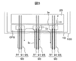
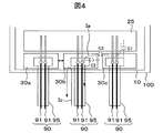
次に、本発明によるノイズ抑止の原理について、図3および図4を参照して説明する。図3に、フレームグランドを共通フレームグランドとした場合を示す。また、図4に、フレームグランドに、本発明を適用して複数の分離領域に分離したものを用いた場合を示す。いずれの場合も、信号グランドのP部に、局所的にノイズ電圧が発生した場合を例として説明する。なお、説明の便宜のため、図1に示す回路基板より簡単な回路構成としてある。
(信号グランドノイズ電流が他の信号線に伝導する場合)
図3に示す共通フレームグランドを用いた回路では、信号グランド25のP部に局所的に発生したノイズ電圧が、ノイズ電流Iaとして、容量C1、C2を通って、信号ケーブル90の信号線91に伝導する。その結果、このノイズ電流に起因して、外部に放射ノイズを発生させ、EMI特性を低下させる。ここで、C1は、信号グランド25と共通フレームグランドCFGとの間の浮遊容量である。また、C2は、共通フレームグランドCFGと信号線91との間の浮遊容量である。
Next, the principle of noise suppression according to the present invention will be described with reference to FIGS. FIG. 3 shows a case where the frame ground is a common frame ground. FIG. 4 shows a case where a frame ground that is separated into a plurality of separation regions by applying the present invention is used. In any case, a case where a noise voltage is locally generated in the P portion of the signal ground will be described as an example. For convenience of explanation, the circuit configuration is simpler than that of the circuit board shown in FIG.
(When signal ground noise current is conducted to other signal lines)
In the circuit using the common frame ground shown in FIG. 3, the noise voltage locally generated at the P portion of the signal ground 25 passes through the capacitors C1 and C2 as the noise current Ia to the
信号グランドのような平板導体の場合、ノイズの平行平板共振によって、強度が局部的大きくなる部分(例えば、P部)が発生する。このようなノイズは、数百メガヘルツと高周波のため、容量C1、C2を通りやすく、外部に伝導しやすい。フレームグランドが共通の場合に、このノイズがすべての信号にのる可能性がある。この場合、ほとんどすべての信号についてフィルタを入れることによって対処することも考えられるが、ノイズ対策が複雑となる。 In the case of a flat conductor such as a signal ground, a portion where the strength is locally increased (for example, a P portion) is generated by parallel plate resonance of noise. Since such noise has a high frequency of several hundred megahertz, it easily passes through the capacitors C1 and C2, and is easily conducted to the outside. If the frame ground is common, this noise can be applied to all signals. In this case, it is conceivable to deal with almost all signals by inserting a filter, but noise countermeasures are complicated.
なお、局部的ノイズとしては、他にLSIの電源電流ノイズ等が考えられる。 In addition, as local noise, LSI power supply current noise and the like can be considered.
これに対して、本発明を適用して、フレームグランドを複数の分離領域30aから30cに分離した場合、図4に示すように、各分離領域30aと30bとの間、30bと30cとの間が、直流的には非導通となる。一方、高周波的にも、浮遊容量C3を小さくすることができることから、ここを通るノイズ電流を小さくすることができる。その結果、ノイズが他の部分に拡散することを防止することができるため、一部の信号についてフィルタを入れるだけで対処することが可能となる。従って、ノイズ対策が非常に簡便なものとなる。
(外部信号のフレームグランドノイズ電流が他の信号のケーブルフレームグランド95または他の信号ラインに伝導する場合)
他の信号のケーブルフレームグランド95または他の信号ラインに伝導したノイズ電流Icは、伝導ノイズまたは放射ノイズとなり、EMI特性を低下させる。フレームグランドが共通の場合、このノイズがすべての信号にのる可能性がある。そのため、すべての信号についてフィルタを入れるなどの対策が必要となる。
On the other hand, when the present invention is applied and the frame ground is separated into a plurality of
(When external signal frame ground noise current is conducted to other signal
The noise current Ic conducted to the
しかし、本発明の場合、フレームグランンドが複数に分離されているため、前述した理由から、ノイズ電流Icがフレームグランド30bから他のフレームグランド(例えば、30a)に流れることがなくなる。そのため、すべてのフレームグランドにノイズがのるという事態になることが避けられる。そのため、一部の信号についてのみノイズ対策をすれば足り、対策が簡便になる。
However, in the case of the present invention, since the frame ground is separated into a plurality, the noise current Ic does not flow from the
なお、以上に述べた本発明が解決しようとする課題は、フレームグランドが筐体に対して浮いている場合でも、また、筐体と接続されている場合でも、同じである。 The problem to be solved by the present invention described above is the same whether the frame ground is floating with respect to the casing or connected to the casing.
次に、接地部材の具体例について説明する。ここでは、連結部材と圧接部材とについて説明する。もちろん、接地部材は、連結部材と圧接部材に限られるものではない。 Next, a specific example of the ground member will be described. Here, the connecting member and the pressure contact member will be described. Of course, the grounding member is not limited to the connecting member and the pressure contact member.
連結部材の一例として、図6に示す形態ものを用いることができる。図6に示す連結部材601は、棒状体601aと、その両端にそれぞれねじ部601bおよび601cとを有する。棒状体601aと、ねじ部601bおよび601cとは、いずれも金属により形成される。また、棒状体601aと、ねじ部601bおよび601cとは、本実施形態では一体に形成されている。この連結部材601を、非金属材料によりその形態を形成し、その表面に金属膜をコーティングして導電性を持たせることにより構成してもよい。
As an example of the connecting member, the one shown in FIG. 6 can be used. A connecting
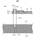
この連結部材601は、ねじ部601cを、筐体100の底面101に設けられているねじ孔102にねじ込み、さらに、他のねじ部601bを、回路基板20に設けられている貫通孔201に通し、かつ、接続パッド204の貫通孔を通して、先端側を回路基板20の上面側に突出させる。このねじ部601bの先端側にナット601dをねじ込んで、連結部材601を回路基板20に固定する。これにより、回路基板31が連結部材601により筐体100に固定される。また、分離領域31(31に限られないが、ここでは代表して31を示す)が、制限回路71と、接続パッド204とを介してナット601dと導通する。その結果、分離領域31、制限回路71、接続パッド204、ナット601d、ねじ部601b、棒状体601a、ねじ部601c、ねじ孔102、筐体100の順に電流路が形成され、分離領域31が筐体100に接地されることとなる。ここでは、すべて導体による電流路が形成される。なお、図6、図7に示すように、回路基板20の裏面側に接続パッド202を設ける構成としてもよい。その場合には、接続パッド202と分離領域31とを導通する手段を別途設けておく。
In this connecting
連結部材としては、この他に、例えば、導電性皮膜をコーティングしたボルト、金属製のボルト、鳩目金具、リード線等の部材が挙げられる。 Other examples of the connecting member include bolts coated with a conductive film, metal bolts, eyelet fittings, lead wires, and the like.
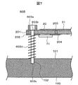
次に、圧接部材の第1の例について、図7を参照して説明する。図7に示す圧接部材603は、頭部603aおよび支持部603bを有するボルト形状の部材と、コイルばね603dとにより構成される。支持部603bは、少なくともその先端側にねじ部603cが設けられている。この圧接部材603は、ボルト形状部分と、コイルばね603dとがいずれも金属により設けられている。
Next, a first example of the pressure contact member will be described with reference to FIG. A
この圧接部材603は、支持部603bを、回路基板20に設けられた貫通孔201に通し、先端側のねじ部603cを、筐体100の底面101に設けられたねじ孔102にねじ込む。その際、支持部603bを、コイルばね603dに通しておく。この状態で、支持部603bのねじ部603cがねじ孔102にねじ込まれると、コイルばね603dが圧縮付勢されて、回路基板20に設けられた接続パッド202と、筐体100の底面101との間で、端部がそれぞれに圧接されることとなる。その結果、回路基板20が固定支持されると共に、接続パッド202がコイルばね603dを介して筐体100に接地されることとなる。
In this
接続パッド202は、分離領域31と導通させておく。接続パッド202は、制限回路71を介して別の接続パッド204に接続される。ここで、接続パッド204は、ビア203を介して、基板表面の分離領域31と導通する。
The
なお、図7の例では、ボルト形状の部材を、導電性を有する部材、例えば、金属により形成することによって、このボルトを介して接地することも可能となる。もちろん、ボルトとコイルばねの両者により接地することも可能である。 In the example of FIG. 7, the bolt-shaped member can be grounded through the bolt by being formed of a conductive member, for example, metal. Of course, it is also possible to ground by both bolts and coil springs.
次に、圧接部材の第2の例について、図8を参照して説明する。図8に示す圧接部材605は、板ばね605aにより構成される。この板ばね605aは、例えば、導線性を有する部材、具体的には金属、さらに具体的には、燐青銅板等により構成することができる。図8の例では、基本的な形状として、板材を二つ折りにした形状を有する。また、その両端部に、電気的接続をより良好とするための接続部605bおよび605cが設けられている。これらの接続部605bおよび605cは、例えば、端面を切削することにより形成される。また、板ばね605aの端部を折り返して平面部とすることにより形成することもできる。
Next, a second example of the pressure contact member will be described with reference to FIG. The
この圧接部材605は、回路基板20と筐体100の底面101との間に配置される。その際、押圧付勢した状態におく。この状態により、圧接部材605は、板ばね605a7が圧縮付勢されて、接続部605bが回路基板20に設けられた接続パッド202と、また、接続部605cが筐体100の底面101と、それぞれ圧接されることとなる。その結果、接続パッド202が、接続部605b、板ばね605a、および、接続部605dを介して筐体100に接地されることとなる。なお、接続パッド202は、分離領域31と導通させておく。また、この例の場合には、回路基板20を固定する他の手段を設けておく必要がある。
The
接続パッド202は、分離領域31と導通させておく。この接続パッド202は、ビア203を介して接続パッド204と接続される。接続パッド204は、制限回路71を介して分離領域31に接続される。
The
なお、図8の例では、板ばね605を金属で形成した例を示したが、これに限られない。例えば、弾性のある絶縁材料により板ばねを形成し、その表面に導電性皮膜をコーティングする構成としてもよい。
In the example of FIG. 8, the example in which the
10…回路基板、11…絶縁層、20…電源/グランドパターン、30…フレームグランド、31−37…分離領域、40…コネクタ端子群、41−47…コネクタ端子、51…電源線、52−57…信号線、61…接地部材、601連結部材、603,605…圧接部材、71…制限回路、100…筐体、201…貫通孔、202、204…接続パッド。
DESCRIPTION OF
Claims (10)
前記回路素子群が搭載される回路基板と、
外部との接続を行うための、複数のコネクタ端子と、
前記回路基板に設けられるフレームグランドと、を有し、
前記フレームグランドは、複数の分離領域に分離された状態で、前記回路基板の縁部に沿って配置され、かつ、前記複数の分離領域は、複数のコネクタ端子に対応して、分散して配置され、
前記分離領域のうち少なくとも一部については、制限回路を介して接地されること
を特徴とする電子回路ユニット。 In the electronic circuit unit in which the circuit element group is mounted and accommodated in the housing of the electronic device,
A circuit board on which the circuit element group is mounted;
Multiple connector terminals for connecting to the outside,
A frame ground provided on the circuit board,
The frame ground is arranged along the edge of the circuit board in a state of being separated into a plurality of separation regions, and the plurality of separation regions are arranged in a distributed manner corresponding to the plurality of connector terminals. And
At least a part of the separation region is grounded via a limiting circuit.
前記制限回路は、抵抗、コンデンサ、抵抗−コンデンサの並列接続回路、および、抵抗−コンデンサの並列接続回路のいずれかを回路素子として有するものであることを特徴とする電子回路ユニット。 The electronic circuit unit according to claim 1,
The electronic circuit unit, wherein the limiting circuit has any one of a resistor, a capacitor, a resistor-capacitor parallel connection circuit, and a resistor-capacitor parallel connection circuit as a circuit element.
前記制限回路は、前記回路素子が素子基板上に形成されたものであることを特徴とする電子回路ユニット。 The electronic circuit unit according to claim 2,
The electronic circuit unit, wherein the limiting circuit is one in which the circuit element is formed on an element substrate.
前記各分離領域は、前記接地を、接地部材を介して行い、
前記制限回路は、前記制限回路を介在させて接地する分離領域において、当該分離回路と対応する接地部材とに接続されることを特徴とする電子回路ユニット。 In the electronic circuit unit according to any one of claims 1, 2, and 3,
Each separation region performs the grounding via a grounding member,
The electronic circuit unit according to claim 1, wherein the limiting circuit is connected to a grounding member corresponding to the separating circuit in a separation region grounded through the limiting circuit.
前記分離領域のいずれかは、前記複数のコネクタ端子のうち、2以上のコネクタ端子に対応して配置されることを特徴とする電子回路ユニット。 In the electronic circuit unit according to any one of claims 1, 2, 3, and 4,
One of the separation regions is arranged corresponding to two or more connector terminals among the plurality of connector terminals.
フレームグランドと、
前記フレームグランドを接地するに用いられる制限回路と、を有し、
前記フレームグランドは、複数の分離領域に分離された状態で、当該回路基板の縁部に沿って配置され、かつ、前記複数の分離領域は、複数のコネクタ端子に対応して、分散して配置され、
前記分離領域のうち少なくとも一部については、前記制限回路を介して接地されること
を特徴とする回路基板。 In circuit boards for mounting circuit element groups and connector terminals,
Frame ground,
A limiting circuit used for grounding the frame ground,
The frame ground is arranged along the edge of the circuit board in a state of being separated into a plurality of separation regions, and the plurality of separation regions are arranged in a distributed manner corresponding to the plurality of connector terminals. And
At least a part of the isolation region is grounded through the limiting circuit.
前記制限回路は、抵抗、コンデンサ、抵抗−コンデンサの並列接続回路、および、抵抗−コンデンサの並列接続回路のいずれかを回路素子として有するものであることを特徴とする回路基板。 The circuit board according to claim 6,
The circuit board, wherein the limiting circuit includes any one of a resistor, a capacitor, a resistor-capacitor parallel connection circuit, and a resistor-capacitor parallel connection circuit as a circuit element.
前記制限回路は、前記回路素子が素子基板上に形成されたものであることを特徴とする回路基板。 The circuit board according to claim 7,
The circuit board, wherein the limiting circuit is one in which the circuit element is formed on an element substrate.
前記接地は、各分離領域対応に接地部材を介して行い、
前記制限回路は、前記制限回路を介在させて接地する分離領域において、当該分離回路と対応する接地部材とに接続されることを特徴とする回路基板。 In the circuit board according to any one of claims 6, 7, and 8,
The grounding is performed via a grounding member corresponding to each separation region,
The circuit board according to claim 1, wherein the limiting circuit is connected to a grounding member corresponding to the separating circuit in a separation region grounded through the limiting circuit.
前記分離領域のいずれかは、前記複数のコネクタ端子のうち、2以上のコネクタ端子に対応して配置されることを特徴とする回路基板。 The circuit board according to any one of claims 6, 7, 8 and 9,
Any of the separation regions is arranged corresponding to two or more connector terminals among the plurality of connector terminals.
Priority Applications (1)
| Application Number | Priority Date | Filing Date | Title |
|---|---|---|---|
| JP2004107073A JP2005294511A (en) | 2004-03-31 | 2004-03-31 | Electronic circuit unit having connector terminal and circuit board |
Applications Claiming Priority (1)
| Application Number | Priority Date | Filing Date | Title |
|---|---|---|---|
| JP2004107073A JP2005294511A (en) | 2004-03-31 | 2004-03-31 | Electronic circuit unit having connector terminal and circuit board |
Related Child Applications (1)
| Application Number | Title | Priority Date | Filing Date |
|---|---|---|---|
| JP2008097741A Division JP2008172280A (en) | 2008-04-04 | 2008-04-04 | Electronic circuit unit having connector terminal and circuit board |
Publications (1)
| Publication Number | Publication Date |
|---|---|
| JP2005294511A true JP2005294511A (en) | 2005-10-20 |
Family
ID=35327109
Family Applications (1)
| Application Number | Title | Priority Date | Filing Date |
|---|---|---|---|
| JP2004107073A Pending JP2005294511A (en) | 2004-03-31 | 2004-03-31 | Electronic circuit unit having connector terminal and circuit board |
Country Status (1)
| Country | Link |
|---|---|
| JP (1) | JP2005294511A (en) |
Cited By (8)
| Publication number | Priority date | Publication date | Assignee | Title |
|---|---|---|---|---|
| JP2008130584A (en) * | 2006-11-16 | 2008-06-05 | Mitsubishi Electric Corp | Electromagnetic noise countermeasure structure for printed circuit boards |
| WO2009063858A1 (en) * | 2007-11-16 | 2009-05-22 | Hamamatsu Photonics K.K. | X-ray image acquiring apparatus |
| JP2009534815A (en) * | 2006-04-20 | 2009-09-24 | ローゼンベルガー ホーフフレクベンツテクニーク ゲーエムベーハー ウント ツェーオー カーゲー | Potential-free penetrating housing |
| US7643750B2 (en) | 2005-10-20 | 2010-01-05 | Ricoh Company, Ltd. | Photographing apparatus with image-blur suppression mechanism |
| US8085548B2 (en) | 2006-09-01 | 2011-12-27 | Hitachi, Ltd. | Circuit for suppressing electromagnetic interference, implementation structure and electronic apparatus implementing the same |
| US8179447B2 (en) | 2007-03-16 | 2012-05-15 | Ricoh Company, Ltd. | Imaging apparatus having blur correction mechanism |
| JP2013222869A (en) * | 2012-04-18 | 2013-10-28 | Hitachi Automotive Systems Ltd | Circuit board of on-vehicle electronic control device |
| JP2021028934A (en) * | 2019-08-09 | 2021-02-25 | キヤノン株式会社 | Printed circuit board |
-
2004
- 2004-03-31 JP JP2004107073A patent/JP2005294511A/en active Pending
Cited By (12)
| Publication number | Priority date | Publication date | Assignee | Title |
|---|---|---|---|---|
| US7643750B2 (en) | 2005-10-20 | 2010-01-05 | Ricoh Company, Ltd. | Photographing apparatus with image-blur suppression mechanism |
| JP2009534815A (en) * | 2006-04-20 | 2009-09-24 | ローゼンベルガー ホーフフレクベンツテクニーク ゲーエムベーハー ウント ツェーオー カーゲー | Potential-free penetrating housing |
| US8085548B2 (en) | 2006-09-01 | 2011-12-27 | Hitachi, Ltd. | Circuit for suppressing electromagnetic interference, implementation structure and electronic apparatus implementing the same |
| JP2008130584A (en) * | 2006-11-16 | 2008-06-05 | Mitsubishi Electric Corp | Electromagnetic noise countermeasure structure for printed circuit boards |
| US8179447B2 (en) | 2007-03-16 | 2012-05-15 | Ricoh Company, Ltd. | Imaging apparatus having blur correction mechanism |
| WO2009063858A1 (en) * | 2007-11-16 | 2009-05-22 | Hamamatsu Photonics K.K. | X-ray image acquiring apparatus |
| JP2009119116A (en) * | 2007-11-16 | 2009-06-04 | Hamamatsu Photonics Kk | X-ray image acquisition device |
| US8265226B2 (en) | 2007-11-16 | 2012-09-11 | Hamamatsu Photonics K.K. | X-ray image acquiring apparatus |
| JP2013222869A (en) * | 2012-04-18 | 2013-10-28 | Hitachi Automotive Systems Ltd | Circuit board of on-vehicle electronic control device |
| JP2021028934A (en) * | 2019-08-09 | 2021-02-25 | キヤノン株式会社 | Printed circuit board |
| US11758643B2 (en) | 2019-08-09 | 2023-09-12 | Canon Kabushiki Kaisha | Printed circuit board and printing apparatus |
| JP7547036B2 (en) | 2019-08-09 | 2024-09-09 | キヤノン株式会社 | Printed Circuit Board |
Similar Documents
| Publication | Publication Date | Title |
|---|---|---|
| US9515027B2 (en) | Printed circuit board | |
| KR101999509B1 (en) | Circuit board | |
| US6873219B2 (en) | Printed circuit board noise attenuation using lossy conductors | |
| US20200045815A1 (en) | Circuit board and electronic device including the same | |
| JP2005294511A (en) | Electronic circuit unit having connector terminal and circuit board | |
| JP2009248635A (en) | On-vehicle electronic device | |
| WO2002037909A2 (en) | Method and apparatus for distributing power to integrated circuits | |
| WO2012039120A4 (en) | Printed circuit board | |
| CN115299184B (en) | Circuit boards and electronic equipment | |
| JP2008172280A (en) | Electronic circuit unit having connector terminal and circuit board | |
| JP2977018B2 (en) | Interface cable connector | |
| US6933805B1 (en) | High density capacitor filter bank with embedded faraday cage | |
| US8208271B2 (en) | Printed board and image formation apparatus | |
| JP2005294502A (en) | Electronic circuit unit having connector terminal and circuit board | |
| JP2002261410A (en) | Printed wiring board and electronic equipment | |
| JP3559706B2 (en) | Electronics | |
| US4908735A (en) | Electronic apparatus reducing generation of electro magnetic interference | |
| US10912187B2 (en) | Printed board | |
| US7626828B1 (en) | Providing a resistive element between reference plane layers in a circuit board | |
| JP3782577B2 (en) | Multilayer printed wiring board and electronic apparatus provided with the wiring board | |
| JP5881849B2 (en) | Electronic device and electromagnetic noise countermeasure method | |
| JP2014007391A (en) | Electronic apparatus | |
| JP2005294501A (en) | Electronic circuit unit having connector terminal and circuit board | |
| JP2000228255A (en) | connector | |
| CN111315115B (en) | Implementation method for preventing secondary electrostatic discharge, circuit board and electronic equipment |
Legal Events
| Date | Code | Title | Description |
|---|---|---|---|
| A977 | Report on retrieval |
Effective date: 20070305 Free format text: JAPANESE INTERMEDIATE CODE: A971007 |
|
| A131 | Notification of reasons for refusal |
Effective date: 20070619 Free format text: JAPANESE INTERMEDIATE CODE: A131 |
|
| A521 | Written amendment |
Free format text: JAPANESE INTERMEDIATE CODE: A523 Effective date: 20070820 |
|
| A02 | Decision of refusal |
Free format text: JAPANESE INTERMEDIATE CODE: A02 Effective date: 20080205 |