JP2005294360A - Manufacturing method of semiconductor device - Google Patents
Manufacturing method of semiconductor device Download PDFInfo
- Publication number
- JP2005294360A JP2005294360A JP2004104041A JP2004104041A JP2005294360A JP 2005294360 A JP2005294360 A JP 2005294360A JP 2004104041 A JP2004104041 A JP 2004104041A JP 2004104041 A JP2004104041 A JP 2004104041A JP 2005294360 A JP2005294360 A JP 2005294360A
- Authority
- JP
- Japan
- Prior art keywords
- mos transistor
- film
- nisi
- semiconductor device
- manufacturing
- Prior art date
- Legal status (The legal status is an assumption and is not a legal conclusion. Google has not performed a legal analysis and makes no representation as to the accuracy of the status listed.)
- Pending
Links
Images

Classifications
-
- H—ELECTRICITY
- H10—SEMICONDUCTOR DEVICES; ELECTRIC SOLID-STATE DEVICES NOT OTHERWISE PROVIDED FOR
- H10D—INORGANIC ELECTRIC SEMICONDUCTOR DEVICES
- H10D30/00—Field-effect transistors [FET]
- H10D30/60—Insulated-gate field-effect transistors [IGFET]
- H10D30/791—Arrangements for exerting mechanical stress on the crystal lattice of the channel regions
-
- H—ELECTRICITY
- H10—SEMICONDUCTOR DEVICES; ELECTRIC SOLID-STATE DEVICES NOT OTHERWISE PROVIDED FOR
- H10D—INORGANIC ELECTRIC SEMICONDUCTOR DEVICES
- H10D30/00—Field-effect transistors [FET]
- H10D30/01—Manufacture or treatment
- H10D30/021—Manufacture or treatment of FETs having insulated gates [IGFET]
- H10D30/0212—Manufacture or treatment of FETs having insulated gates [IGFET] using self-aligned silicidation
-
- H—ELECTRICITY
- H10—SEMICONDUCTOR DEVICES; ELECTRIC SOLID-STATE DEVICES NOT OTHERWISE PROVIDED FOR
- H10D—INORGANIC ELECTRIC SEMICONDUCTOR DEVICES
- H10D64/00—Electrodes of devices having potential barriers
- H10D64/01—Manufacture or treatment
- H10D64/011—Manufacture or treatment of electrodes ohmically coupled to a semiconductor
- H10D64/0111—Manufacture or treatment of electrodes ohmically coupled to a semiconductor to Group IV semiconductors
- H10D64/0112—Manufacture or treatment of electrodes ohmically coupled to a semiconductor to Group IV semiconductors using conductive layers comprising silicides
-
- H—ELECTRICITY
- H10—SEMICONDUCTOR DEVICES; ELECTRIC SOLID-STATE DEVICES NOT OTHERWISE PROVIDED FOR
- H10D—INORGANIC ELECTRIC SEMICONDUCTOR DEVICES
- H10D84/00—Integrated devices formed in or on semiconductor substrates that comprise only semiconducting layers, e.g. on Si wafers or on GaAs-on-Si wafers
- H10D84/01—Manufacture or treatment
- H10D84/0123—Integrating together multiple components covered by H10D12/00 or H10D30/00, e.g. integrating multiple IGBTs
- H10D84/0126—Integrating together multiple components covered by H10D12/00 or H10D30/00, e.g. integrating multiple IGBTs the components including insulated gates, e.g. IGFETs
- H10D84/0165—Integrating together multiple components covered by H10D12/00 or H10D30/00, e.g. integrating multiple IGBTs the components including insulated gates, e.g. IGFETs the components including complementary IGFETs, e.g. CMOS devices
- H10D84/0172—Manufacturing their gate conductors
- H10D84/0174—Manufacturing their gate conductors the gate conductors being silicided
-
- H—ELECTRICITY
- H10—SEMICONDUCTOR DEVICES; ELECTRIC SOLID-STATE DEVICES NOT OTHERWISE PROVIDED FOR
- H10D—INORGANIC ELECTRIC SEMICONDUCTOR DEVICES
- H10D84/00—Integrated devices formed in or on semiconductor substrates that comprise only semiconducting layers, e.g. on Si wafers or on GaAs-on-Si wafers
- H10D84/01—Manufacture or treatment
- H10D84/02—Manufacture or treatment characterised by using material-based technologies
- H10D84/03—Manufacture or treatment characterised by using material-based technologies using Group IV technology, e.g. silicon technology or silicon-carbide [SiC] technology
- H10D84/038—Manufacture or treatment characterised by using material-based technologies using Group IV technology, e.g. silicon technology or silicon-carbide [SiC] technology using silicon technology, e.g. SiGe
-
- H—ELECTRICITY
- H10—SEMICONDUCTOR DEVICES; ELECTRIC SOLID-STATE DEVICES NOT OTHERWISE PROVIDED FOR
- H10D—INORGANIC ELECTRIC SEMICONDUCTOR DEVICES
- H10D30/00—Field-effect transistors [FET]
- H10D30/60—Insulated-gate field-effect transistors [IGFET]
- H10D30/601—Insulated-gate field-effect transistors [IGFET] having lightly-doped drain or source extensions, e.g. LDD IGFETs or DDD IGFETs
Landscapes
- Metal-Oxide And Bipolar Metal-Oxide Semiconductor Integrated Circuits (AREA)
- Electrodes Of Semiconductors (AREA)
- Insulated Gate Type Field-Effect Transistor (AREA)
Abstract
【課題】 NiSi膜のダイシリサイド化を抑制することのできる半導体装置の製造方法を提供する。
【解決手段】 P−MOSトランジスタ10およびN−MOSトランジスタ20双方のゲート電極12,22およびソース・ドレイン領域14,24上にNiSi膜42を形成する(シリサイド膜形成工程)。次に、NiSi膜42を含めた表面全体にダイレクト窒化膜44を形成する(窒化膜形成工程)。続いて、NiSi膜42の耐熱温度を高める元素をNiSi膜42に注入する(元素注入工程)。これにより、NiSi膜42の耐熱性が向上し、後工程における熱処理によりNiSi膜42がダイシリサイド化するのを抑制することができる。
【選択図】 図5
PROBLEM TO BE SOLVED: To provide a manufacturing method of a semiconductor device capable of suppressing disilicidation of a NiSi film.
An NiSi film is formed on gate electrodes 12 and 22 and source / drain regions 14 and 24 of both a P-MOS transistor 10 and an N-MOS transistor 20 (silicide film forming step). Next, a direct nitride film 44 is formed on the entire surface including the NiSi film 42 (nitride film forming step). Subsequently, an element for increasing the heat resistance temperature of the NiSi film 42 is implanted into the NiSi film 42 (element implantation step). Thereby, the heat resistance of the NiSi film 42 can be improved, and the NiSi film 42 can be prevented from being disilicided by heat treatment in a later process.
[Selection] Figure 5
Description
本発明は、半導体装置の製造方法に関するものである。 The present invention relates to a method for manufacturing a semiconductor device.
従来の半導体装置の製造方法としては、例えば特許文献1に開示されたものがある。同文献に記載の製造方法は、素子の寄生抵抗を低減するために、MOSトランジスタのゲート電極上およびソース・ドレイン電極上にNiSiからなるモノシリサイド膜を形成する工程を含んでいる。
しかしながら、上記製造方法においては、後工程における熱処理によりNiSi膜がダイシリサイド化するおそれがある。NiSi膜がダイシリサイド化した場合、MOSトランジスタの寄生抵抗の増大等につながってしまう。 However, in the above manufacturing method, there is a possibility that the NiSi film may be disilicided by a heat treatment in a later process. When the NiSi film is disilicided, this leads to an increase in parasitic resistance of the MOS transistor.
本発明は、上記課題に鑑みてなされたものであり、半導体装置に用いられるNiSi膜の耐熱性を高め、ダイシリサイド化を抑制し、これにより半導体装置の性能を向上させることを目的とする。 The present invention has been made in view of the above problems, and an object of the present invention is to improve the heat resistance of a NiSi film used in a semiconductor device, suppress disilicide formation, and thereby improve the performance of the semiconductor device.
上記課題を解決する本発明によれば、MOSトランジスタを備える半導体装置を製造する方法であって、前記MOSトランジスタのゲート電極およびソース・ドレイン領域の少なくとも一方の上にNiSi膜を形成するシリサイド膜形成工程と、前記NiSi膜のダイシリサイド化を抑制する反応抑制元素を前記NiSi膜に注入する元素注入工程と、を含むことを特徴とする半導体装置の製造方法が提供される。 According to the present invention for solving the above-mentioned problems, there is provided a method of manufacturing a semiconductor device comprising a MOS transistor, wherein a silicide film is formed by forming a NiSi film on at least one of a gate electrode and a source / drain region of the MOS transistor. There is provided a method for manufacturing a semiconductor device, comprising: a step; and an element injection step of injecting a reaction suppressing element that suppresses disilicideation of the NiSi film into the NiSi film.
この製造方法においては、元素注入工程において、NiSi膜のダイシリサイド化を抑制する反応抑制元素がNiSi膜中に導入される。これにより、NiSi膜の耐熱性が向上し、後工程における熱処理によりNiSi膜がダイシリサイド化するのを抑制することができる。 In this manufacturing method, a reaction suppressing element that suppresses disilicideation of the NiSi film is introduced into the NiSi film in the element implantation step. Thereby, the heat resistance of the NiSi film is improved, and the NiSi film can be prevented from being disilicided by the heat treatment in the subsequent process.
NiSi膜上にダイレクト窒化膜を形成する窒化膜形成工程を含み、元素注入工程においては、元素がNiSi膜に到達するように、ダイレクト窒化膜上から上記元素を注入してもよい。この場合、ダイシリサイド化の抑制とともに、ダイレクト窒化膜の応力を緩和することが可能となる。 A nitride film forming step of forming a direct nitride film on the NiSi film may be included, and the element may be implanted from the direct nitride film so that the element reaches the NiSi film in the element implantation step. In this case, it is possible to reduce the stress of the direct nitride film as well as suppress disilicide.
本発明において、半導体装置は、P−MOSトランジスタおよびN−MOSトランジスタを備え、ダイレクト窒化膜はテンサイル応力を持つものであり、元素注入工程においては、P−MOSトランジスタおよびN−MOSトランジスタのうちP−MOSトランジスタに形成されたNiSi膜にのみ上記元素を注入してもよい。ダイレクト窒化膜がテンサイル応力を持つ場合、N−MOSトランジスタのオン電流が向上する一方で、P−MOSトランジスタのオン電流は低下してしまう。したがって、元素注入工程においてP−MOSトランジスタ側にのみ元素注入を行うことにより、テンサイル応力が緩和され、P−MOSトランジスタのオン電流の低下が抑制される。 In the present invention, the semiconductor device includes a P-MOS transistor and an N-MOS transistor, and the direct nitride film has a tensile stress. In the element implantation process, the P-MOS transistor and the N-MOS transistor include P The element may be implanted only into the NiSi film formed in the MOS transistor. When the direct nitride film has a tensile stress, the on-current of the N-MOS transistor is improved while the on-current of the P-MOS transistor is lowered. Therefore, by performing the element implantation only on the P-MOS transistor side in the element implantation step, the tensile stress is relieved and the decrease in the on-current of the P-MOS transistor is suppressed.
本発明において、半導体装置は、P−MOSトランジスタおよびN−MOSトランジスタを備え、ダイレクト窒化膜はコンプレッシブ応力を持つものであり、元素注入工程においては、P−MOSトランジスタおよびN−MOSトランジスタのうちN−MOSトランジスタに形成されたNiSi膜にのみ上記元素を注入してもよい。ダイレクト窒化膜がコンプレッシブ応力を持つ場合、P−MOSトランジスタのオン電流が向上する一方で、N−MOSトランジスタのオン電流は低下してしまう。したがって、元素注入工程においてN−MOSトランジスタ側にのみ元素注入を行うことにより、コンプレッシブ応力が緩和され、N−MOSトランジスタのオン電流の低下が抑制される。 In the present invention, the semiconductor device includes a P-MOS transistor and an N-MOS transistor, and the direct nitride film has a compressive stress. In the element implantation step, the P-MOS transistor and the N-MOS transistor The element may be implanted only into the NiSi film formed in the N-MOS transistor. When the direct nitride film has a compressive stress, the on-current of the P-MOS transistor is improved while the on-current of the N-MOS transistor is lowered. Therefore, by performing the element implantation only on the N-MOS transistor side in the element implantation step, the compressive stress is relieved and the decrease in the on-current of the N-MOS transistor is suppressed.
NiSi膜は、NiSiであってもよい。NiSiは抵抗が低いため、シリサイド膜として好適に機能することができる。 The NiSi film may be NiSi. Since NiSi has a low resistance, it can function suitably as a silicide film.
上記元素は、Ge、N、F、OおよびCからなる群より選ばれる1または2以上の元素であってもよい。これらの元素は、NiSi膜の耐熱温度の向上によるダイシリサイド化の抑制およびダイレクト窒化膜の応力緩和に資するものである。 The element may be one or more elements selected from the group consisting of Ge, N, F, O and C. These elements contribute to the suppression of disilicide by improving the heat-resistant temperature of the NiSi film and the stress relaxation of the direct nitride film.
本発明によれば、NiSi膜のダイシリサイド化を抑制することのできる半導体装置の製造方法が実現される。 According to the present invention, a method of manufacturing a semiconductor device that can suppress disilicideation of a NiSi film is realized.
以下、図面を参照しつつ、本発明による半導体装置の製造方法の好適な実施形態について詳細に説明する。なお、図面の説明においては、同一要素には同一符号を付し、重複する説明を省略する。 Hereinafter, preferred embodiments of a method of manufacturing a semiconductor device according to the present invention will be described in detail with reference to the drawings. In the description of the drawings, the same reference numerals are assigned to the same elements, and duplicate descriptions are omitted.
図1〜図6を用いて、本発明による半導体装置の製造方法の一実施形態を説明する。本実施形態において製造される半導体装置は、P−MOSトランジスタおよびN−MOSトランジスタを備えるCMOSトランジスタ装置である。 An embodiment of a method for manufacturing a semiconductor device according to the present invention will be described with reference to FIGS. The semiconductor device manufactured in this embodiment is a CMOS transistor device including a P-MOS transistor and an N-MOS transistor.
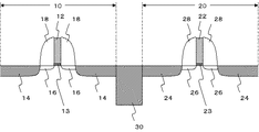
まず、図1に示すように、P−MOSトランジスタ10およびN−MOSトランジスタ20を形成する。P−MOSトランジスタ10は、ゲート電極12、ゲート酸化膜13、ソース・ドレイン領域14、LDD(Lightly Doped Drain)領域16およびスペーサ18を有している。同様に、N−MOSトランジスタ20は、ゲート電極22、ゲート酸化膜23、ソース・ドレイン領域24、LDD領域26およびスペーサ28を有している。P−MOSトランジスタ10とN−MOSトランジスタ20とは、素子分離領域であるSTI(シャロートレンチアイソレーション)領域30によって互いに分離されている。
First, as shown in FIG. 1, a P-
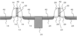
次に、図2に示すように、P−MOSトランジスタ10およびN−MOSトランジスタ20双方のゲート電極12,22およびソース・ドレイン領域14,24上にモノシリサイド膜としてNiSi膜42を形成する(シリサイド膜形成工程)。ただし、NiSi膜42は、ゲート電極12,22およびソース・ドレイン領域のうち何れか一方にのみ形成してもよい。
Next, as shown in FIG. 2, a NiSi
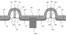
次に、図3に示すように、NiSi膜42を含めた表面全体にダイレクト窒化膜44(層間窒化膜)を形成する(窒化膜形成工程)。このダイレクト窒化膜44は、後述する層間酸化膜46と共に層間絶縁膜を構成するものである。また、本実施形態においてダイレクト窒化膜44は、テンサイル応力を持っている。ダイレクト窒化膜44としては、例えばSiNを用いることができる。
Next, as shown in FIG. 3, a direct nitride film 44 (interlayer nitride film) is formed on the entire surface including the NiSi film 42 (nitride film forming step). This
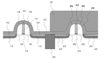
次に、図4に示すように、フォトレジストを用いてN−MOSトランジスタ20全体にマスクMを形成する。
Next, as shown in FIG. 4, a mask M is formed over the entire N-
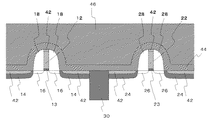
続いて、図5に示すように、NiSi膜42の耐熱温度を高める元素(以下、反応抑制元素という)をNiSi膜42に注入する(元素注入工程)。このとき、N−MOSトランジスタ20側はマスクMにより覆われているため、P−MOSトランジスタ10側にのみ反応抑制元素が注入される。注入条件は、反応抑制元素がNiSi膜42まで到達するように設定される。反応抑制元素としては、例えばGe、N、F、OおよびCが挙げられる。これらの元素は、NiSi膜42の耐熱温度を高め、ダイシリサイド化反応を抑制する働きを有する上、ダイレクト窒化膜44の応力を緩和することもできる。なお、反応抑制元素のうち何れか1つを注入してもよく、複数組み合わせて注入してもよい。
Subsequently, as shown in FIG. 5, an element that raises the heat resistance temperature of the NiSi film 42 (hereinafter referred to as a reaction suppressing element) is implanted into the NiSi film 42 (element implantation step). At this time, since the N-
最後に、図6に示すように、ダイレクト窒化膜44上に層間酸化膜46を形成する。層間酸化膜46としては、例えばSiO2を用いることができる。
Finally, an interlayer oxide film 46 is formed on the
本実施形態に係る製造方法の効果を説明する。 The effects of the manufacturing method according to this embodiment will be described.
上記製造方法においては、元素注入工程において反応抑制元素をNiSi膜42に注入している。これにより、NiSi膜42の耐熱性が向上し、後工程における熱処理によりNiSi膜42がダイシリサイド化するのを抑制することができる。NiSi2はNiSiに比してシート抵抗値が高いため、NiSiのダイシリサイド化を防ぐことは、素子の寄生抵抗を低減する上で非常に重要である。また、NiSiのダイシリサイド化はリーク電流の増大にもつながるが、上記製造方法によれば、このようなリーク電流の増大をも抑制することができる。
In the above manufacturing method, the reaction suppressing element is injected into the NiSi
また、NiSi膜42への反応抑制元素の導入を、NiSi膜42の形成後に注入を行うことにより実行している。このため、P−MOSトランジスタ10への注入量とN−MOSトランジスタ20への注入量とを別々に制御することが容易となる。例えば、本実施形態においては、マスクMを用いることにより、P−MOSトランジスタ10およびN−MOSトランジスタ20のうちP−MOSトランジスタ10に形成されたNiSi膜42にのみ注入を行うことを容易に実現している。
In addition, introduction of the reaction suppressing element into the NiSi
ところで、NiSi膜に反応抑制元素を導入する方法としては、Ni膜成膜時のスパッタガスに反応抑制元素を混入させることも考えられる。しかし、その方法は、P−MOSトランジスタ10側のNiSi膜42とN−MOSトランジスタ20側のNiSi膜42とでNiSi膜42に反応抑制元素の導入量を別々に制御することができないため、好ましくない。しかも、例えばN−MOSトランジスタ20側に不純物元素としてAsが導入されている場合、AsもまたNiSiの耐熱温度を高める働きを持つ元素であるため、スパッタによりP−MOSトランジスタ10側とN−MOSトランジスタ20側とに同量の反応抑制元素を導入してしまうと、結果として、NiSiの耐熱温度を高める元素がP−MOSトランジスタ10側に比してN−MOSトランジスタ20側により多く導入されることになる。すると、NiSi膜を形成する際に、P−MOSトランジスタ10およびN−MOSトランジスタ20間で反応温度のバランスが取りにくくなってしまうという問題がある。
By the way, as a method of introducing the reaction suppressing element into the NiSi film, it is conceivable to mix the reaction suppressing element into the sputtering gas when forming the Ni film. However, this method is preferable because the amount of reaction-inhibiting elements introduced into the NiSi
これに対して、NiSi膜42の形成後に反応抑制元素の注入を行う本実施形態によれば、NiSi膜42の形成時には反応抑制元素が未だ導入されていないため、かかる問題を防ぐことができる。
On the other hand, according to the present embodiment in which the reaction suppressing element is injected after the NiSi
さらに、元素注入工程においては、反応抑制元素がNiSi膜42まで到達するような注入条件に設定される。ここで、基板への導入ダメージやゲート酸化膜への影響を考慮すると、基板やゲート酸化膜には反応抑制元素が注入されないことが望ましい。この点、注入は金属中では止まり易いため、反応抑制元素がNiSi膜42中で止まるように注入条件を設定することは容易である。
Further, in the element implantation step, the implantation conditions are set such that the reaction suppressing element reaches the
特に、本実施形態においては、ダイレクト窒化膜44上から反応抑制元素を注入している。これにより、NiSi膜42のダイシリサイド化の抑制とともに、ダイレクト窒化膜44の応力を緩和することができる。
In particular, in the present embodiment, the reaction suppressing element is implanted from above the
また、P−MOSトランジスタ10に形成されたNiSi膜42にのみ反応抑制元素を注入している。ダイレクト窒化膜44は、テンサイル応力を持っているため、N−MOSトランジスタのオン電流を向上させる一方で、P−MOSトランジスタのオン電流を低下させる。したがって、P−MOSトランジスタ10側にのみ元素注入を行うことにより、P−MOSのオン電流の低下を抑制することができる。
Further, a reaction suppressing element is implanted only into the
なお、上記実施形態においてはテンサイル応力を持つダイレクト窒化膜を用い、P−MOSトランジスタ10側にのみ反応抑制元素を注入する例を示したが、コンプレッシブ応力を持つダイレクト窒化膜を用い、N−MOSトランジスタ20側にのみ反応抑制元素を注入することとしてもよい。
In the above embodiment, a direct nitride film having a tensile stress is used and a reaction suppressing element is injected only into the P-
また、本実施形態においては、ダイレクト窒化膜44と層間酸化膜46とを積層させた構造の層間絶縁膜を形成している。これにより、コンタクト形成等のため層間絶縁膜をエッチングする際に、ダイレクト窒化膜44をエッチングストッパとして機能させることができる。ただし、ダイレクト窒化膜44を設けることは必須ではない。ダイレクト窒化膜44を設けない場合すなわち窒化膜形成工程を省略する場合には、シリサイド膜形成工程の直後に元素注入工程を実行すればよい。このとき、P−MOSトランジスタ10側およびN−MOSトランジスタ20側の双方に反応抑制元素を注入してもよく、何れか一方にのみ注入してもよい。
In the present embodiment, an interlayer insulating film having a structure in which the
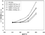
図7は、NiSi膜に反応抑制元素を注入した場合および注入しない場合それぞれについて、NiSi膜の耐熱温度を測定したグラフである。反応抑制元素の注入は、ダイレクト窒化膜上から行った。ここでいう耐熱温度とは、NiSi膜が、ダイシリサイド化すなわちNiSi2膜に変化するときの温度である。グラフの縦軸はシート抵抗値(Ω/□)を表し、横軸は温度(℃)を表す。ニッケルがダイシリサイド化するとシート抵抗値が増大することから、注入なしの場合の耐熱温度が約450℃であるのに対し、反応抑制元素を注入した場合の耐熱温度は500℃以上であることが判る。したがって、反応抑制元素を注入することにより、NiSi膜の耐熱性を向上させることができ、それによりNiSi膜のダイシリサイド化を抑制することができる。 FIG. 7 is a graph obtained by measuring the heat-resistant temperature of the NiSi film when the reaction suppressing element is injected into the NiSi film and when it is not injected. The reaction suppressing element was injected from the direct nitride film. The heat-resistant temperature here is a temperature at which the NiSi film changes to disilicide, that is, a NiSi 2 film. The vertical axis of the graph represents the sheet resistance value (Ω / □), and the horizontal axis represents the temperature (° C.). Since the sheet resistance value increases when nickel is disilicided, the heat resistance temperature without implantation is about 450 ° C., whereas the heat resistance temperature when reaction-suppressing elements are implanted is 500 ° C. or higher. I understand. Therefore, by injecting the reaction suppressing element, the heat resistance of the NiSi film can be improved, and thereby the disilicideation of the NiSi film can be suppressed.
10 P−MOSトランジスタ
12 ゲート電極
13 ゲート酸化膜
14 ソース・ドレイン領域
16 LDD領域
18 スペーサ
20 N−MOSトランジスタ
22 ゲート電極
23 ゲート酸化膜
24 ソース・ドレイン領域
26 LDD領域
28 スペーサ
30 STI領域
42 SiNi膜
44 ダイレクト窒化膜
46 層間酸化膜
10 P-
Claims (5)
前記MOSトランジスタのゲート電極およびソース・ドレイン領域の少なくとも一方の上にNiSi膜を形成するシリサイド膜形成工程と、
前記NiSi膜のダイシリサイド化を抑制する反応抑制元素を前記NiSi膜に注入する元素注入工程と、
を含むことを特徴とする半導体装置の製造方法。 A method of manufacturing a semiconductor device comprising a MOS transistor,
A silicide film forming step of forming a NiSi film on at least one of a gate electrode and a source / drain region of the MOS transistor;
An element injection step of injecting into the NiSi film a reaction suppressing element that suppresses disilicideation of the NiSi film;
A method for manufacturing a semiconductor device, comprising:
前記NiSi膜上に層間窒化膜を形成する窒化膜形成工程を含み、
前記元素注入工程においては、前記元素が前記NiSi膜に到達するように、前記層間窒化膜上から前記元素を注入することを特徴とする半導体装置の製造方法。 A method of manufacturing a semiconductor device according to claim 1,
Including a nitride film forming step of forming an interlayer nitride film on the NiSi film,
In the element implantation step, the element is implanted from above the interlayer nitride film so that the element reaches the NiSi film.
前記半導体装置は、P−MOSトランジスタおよびN−MOSトランジスタを備え、
前記層間窒化膜はテンサイル応力を持つものであり、
前記元素注入工程においては、前記P−MOSトランジスタおよび前記N−MOSトランジスタのうち前記P−MOSトランジスタに形成された前記NiSi膜にのみ前記元素を注入することを特徴とする半導体装置の製造方法。 A method of manufacturing a semiconductor device according to claim 2,
The semiconductor device includes a P-MOS transistor and an N-MOS transistor,
The interlayer nitride film has a tensile stress,
In the element implantation step, the element is implanted only into the NiSi film formed in the P-MOS transistor of the P-MOS transistor and the N-MOS transistor.
前記半導体装置は、P−MOSトランジスタおよびN−MOSトランジスタを備え、
前記層間窒化膜はコンプレッシブ応力を持つものであり、
前記元素注入工程においては、前記P−MOSトランジスタおよび前記N−MOSトランジスタのうち前記N−MOSトランジスタに形成された前記NiSi膜にのみ前記元素を注入することを特徴とする半導体装置の製造方法。 A method of manufacturing a semiconductor device according to claim 2,
The semiconductor device includes a P-MOS transistor and an N-MOS transistor,
The interlayer nitride film has a compressive stress,
In the element implantation step, the element is implanted only into the NiSi film formed in the N-MOS transistor of the P-MOS transistor and the N-MOS transistor.
前記反応抑制元素は、Ge、N、F、OおよびCからなる群より選ばれる1または2以上の元素であることを特徴とする半導体装置の製造方法。 A method for manufacturing a semiconductor device according to any one of claims 1 to 4,
The method of manufacturing a semiconductor device, wherein the reaction suppressing element is one or more elements selected from the group consisting of Ge, N, F, O, and C.
Priority Applications (3)
| Application Number | Priority Date | Filing Date | Title |
|---|---|---|---|
| JP2004104041A JP2005294360A (en) | 2004-03-31 | 2004-03-31 | Manufacturing method of semiconductor device |
| CNB2005100625263A CN100377322C (en) | 2004-03-31 | 2005-03-29 | Method for manufacturing semiconductor device |
| US11/094,393 US7348273B2 (en) | 2004-03-31 | 2005-03-31 | Method of manufacturing a semiconductor device |
Applications Claiming Priority (1)
| Application Number | Priority Date | Filing Date | Title |
|---|---|---|---|
| JP2004104041A JP2005294360A (en) | 2004-03-31 | 2004-03-31 | Manufacturing method of semiconductor device |
Publications (1)
| Publication Number | Publication Date |
|---|---|
| JP2005294360A true JP2005294360A (en) | 2005-10-20 |
Family
ID=35050044
Family Applications (1)
| Application Number | Title | Priority Date | Filing Date |
|---|---|---|---|
| JP2004104041A Pending JP2005294360A (en) | 2004-03-31 | 2004-03-31 | Manufacturing method of semiconductor device |
Country Status (3)
| Country | Link |
|---|---|
| US (1) | US7348273B2 (en) |
| JP (1) | JP2005294360A (en) |
| CN (1) | CN100377322C (en) |
Cited By (8)
| Publication number | Priority date | Publication date | Assignee | Title |
|---|---|---|---|---|
| WO2007055095A1 (en) * | 2005-11-14 | 2007-05-18 | Nec Corporation | Semiconductor device and method for manufacturing same |
| WO2007074775A1 (en) * | 2005-12-26 | 2007-07-05 | Nec Corporation | Nmosfet and method for manufacturing same, and cmosfet and method for manufacturing same |
| WO2007077814A1 (en) * | 2006-01-06 | 2007-07-12 | Nec Corporation | Semiconductor device and process for producing the same |
| WO2007122667A1 (en) * | 2006-03-29 | 2007-11-01 | Fujitsu Limited | Semiconductor device and its manufacturing method |
| JP2007294496A (en) * | 2006-04-21 | 2007-11-08 | Renesas Technology Corp | Semiconductor device and its fabrication process |
| WO2008035490A1 (en) * | 2006-09-20 | 2008-03-27 | Nec Corporation | Semiconductor device and method for manufacturing same |
| JP2009522796A (en) * | 2006-01-09 | 2009-06-11 | インターナショナル・ビジネス・マシーンズ・コーポレーション | Semiconductor device structure having low and high performance devices of the same conductivity type on the same substrate |
| WO2009157042A1 (en) * | 2008-06-26 | 2009-12-30 | 富士通マイクロエレクトロニクス株式会社 | Semiconductor device and method for manufacturing the same |
Families Citing this family (4)
| Publication number | Priority date | Publication date | Assignee | Title |
|---|---|---|---|---|
| US7297584B2 (en) * | 2005-10-07 | 2007-11-20 | Samsung Electronics Co., Ltd. | Methods of fabricating semiconductor devices having a dual stress liner |
| JP4755894B2 (en) * | 2005-12-16 | 2011-08-24 | 株式会社東芝 | Semiconductor device and manufacturing method thereof |
| US7473623B2 (en) * | 2006-06-30 | 2009-01-06 | Advanced Micro Devices, Inc. | Providing stress uniformity in a semiconductor device |
| US8470700B2 (en) * | 2010-07-22 | 2013-06-25 | Globalfoundries Singapore Pte. Ltd. | Semiconductor device with reduced contact resistance and method of manufacturing thereof |
Citations (4)
| Publication number | Priority date | Publication date | Assignee | Title |
|---|---|---|---|---|
| JP2001250791A (en) * | 2000-03-03 | 2001-09-14 | Mitsubishi Electric Corp | Semiconductor device and method of manufacturing the same |
| JP2001352058A (en) * | 2000-06-09 | 2001-12-21 | Toshiba Corp | Method for manufacturing semiconductor device |
| WO2002043151A1 (en) * | 2000-11-22 | 2002-05-30 | Hitachi, Ltd | Semiconductor device and method for fabricating the same |
| JP2002184717A (en) * | 2000-10-02 | 2002-06-28 | Matsushita Electric Ind Co Ltd | Semiconductor device and manufacturing method thereof |
Family Cites Families (16)
| Publication number | Priority date | Publication date | Assignee | Title |
|---|---|---|---|---|
| JPH0590293A (en) | 1991-07-19 | 1993-04-09 | Toshiba Corp | Semiconductor device and manufacturing method thereof |
| US5937315A (en) * | 1997-11-07 | 1999-08-10 | Advanced Micro Devices, Inc. | Self-aligned silicide gate technology for advanced submicron MOS devices |
| US6180469B1 (en) * | 1998-11-06 | 2001-01-30 | Advanced Micro Devices, Inc. | Low resistance salicide technology with reduced silicon consumption |
| US6274511B1 (en) * | 1999-02-24 | 2001-08-14 | Advanced Micro Devices, Inc. | Method of forming junction-leakage free metal silicide in a semiconductor wafer by amorphization of refractory metal layer |
| US6255214B1 (en) * | 1999-02-24 | 2001-07-03 | Advanced Micro Devices, Inc. | Method of forming junction-leakage free metal silicide in a semiconductor wafer by amorphization of source and drain regions |
| US6586333B1 (en) * | 2000-10-05 | 2003-07-01 | Advanced Micro Devices, Inc. | Integrated plasma treatment and nickel deposition and tool for performing same |
| US6890854B2 (en) * | 2000-11-29 | 2005-05-10 | Chartered Semiconductor Manufacturing, Inc. | Method and apparatus for performing nickel salicidation |
| US6605513B2 (en) * | 2000-12-06 | 2003-08-12 | Advanced Micro Devices, Inc. | Method of forming nickel silicide using a one-step rapid thermal anneal process and backend processing |
| US6444578B1 (en) * | 2001-02-21 | 2002-09-03 | International Business Machines Corporation | Self-aligned silicide process for reduction of Si consumption in shallow junction and thin SOI electronic devices |
| US6689688B2 (en) * | 2002-06-25 | 2004-02-10 | Advanced Micro Devices, Inc. | Method and device using silicide contacts for semiconductor processing |
| CN100437970C (en) * | 2003-03-07 | 2008-11-26 | 琥珀波系统公司 | A structure and method for forming a semiconductor structure |
| US20050090067A1 (en) * | 2003-10-27 | 2005-04-28 | Dharmesh Jawarani | Silicide formation for a semiconductor device |
| US6977194B2 (en) * | 2003-10-30 | 2005-12-20 | International Business Machines Corporation | Structure and method to improve channel mobility by gate electrode stress modification |
| US7262105B2 (en) * | 2003-11-21 | 2007-08-28 | Freescale Semiconductor, Inc. | Semiconductor device with silicided source/drains |
| US7105429B2 (en) * | 2004-03-10 | 2006-09-12 | Freescale Semiconductor, Inc. | Method of inhibiting metal silicide encroachment in a transistor |
| US7078285B1 (en) * | 2005-01-21 | 2006-07-18 | Sony Corporation | SiGe nickel barrier structure employed in a CMOS device to prevent excess diffusion of nickel used in the silicide material |
-
2004
- 2004-03-31 JP JP2004104041A patent/JP2005294360A/en active Pending
-
2005
- 2005-03-29 CN CNB2005100625263A patent/CN100377322C/en not_active Expired - Fee Related
- 2005-03-31 US US11/094,393 patent/US7348273B2/en not_active Expired - Fee Related
Patent Citations (4)
| Publication number | Priority date | Publication date | Assignee | Title |
|---|---|---|---|---|
| JP2001250791A (en) * | 2000-03-03 | 2001-09-14 | Mitsubishi Electric Corp | Semiconductor device and method of manufacturing the same |
| JP2001352058A (en) * | 2000-06-09 | 2001-12-21 | Toshiba Corp | Method for manufacturing semiconductor device |
| JP2002184717A (en) * | 2000-10-02 | 2002-06-28 | Matsushita Electric Ind Co Ltd | Semiconductor device and manufacturing method thereof |
| WO2002043151A1 (en) * | 2000-11-22 | 2002-05-30 | Hitachi, Ltd | Semiconductor device and method for fabricating the same |
Cited By (16)
| Publication number | Priority date | Publication date | Assignee | Title |
|---|---|---|---|---|
| US7786537B2 (en) | 2005-11-14 | 2010-08-31 | Nec Corporation | Semiconductor device and method for manufacturing same |
| WO2007055095A1 (en) * | 2005-11-14 | 2007-05-18 | Nec Corporation | Semiconductor device and method for manufacturing same |
| JP5056418B2 (en) * | 2005-11-14 | 2012-10-24 | 日本電気株式会社 | Semiconductor device and manufacturing method thereof |
| WO2007074775A1 (en) * | 2005-12-26 | 2007-07-05 | Nec Corporation | Nmosfet and method for manufacturing same, and cmosfet and method for manufacturing same |
| WO2007077814A1 (en) * | 2006-01-06 | 2007-07-12 | Nec Corporation | Semiconductor device and process for producing the same |
| JPWO2007077814A1 (en) * | 2006-01-06 | 2009-06-11 | 日本電気株式会社 | Semiconductor device and manufacturing method thereof |
| US7968947B2 (en) | 2006-01-06 | 2011-06-28 | Nec Corporation | Semiconductor device and manufacturing process therefor |
| JP2009522796A (en) * | 2006-01-09 | 2009-06-11 | インターナショナル・ビジネス・マシーンズ・コーポレーション | Semiconductor device structure having low and high performance devices of the same conductivity type on the same substrate |
| WO2007122667A1 (en) * | 2006-03-29 | 2007-11-01 | Fujitsu Limited | Semiconductor device and its manufacturing method |
| JP2007294496A (en) * | 2006-04-21 | 2007-11-08 | Renesas Technology Corp | Semiconductor device and its fabrication process |
| JPWO2008035490A1 (en) * | 2006-09-20 | 2010-01-28 | 日本電気株式会社 | Semiconductor device and manufacturing method thereof |
| US7875935B2 (en) | 2006-09-20 | 2011-01-25 | Nec Corporation | Semiconductor device and method for manufacturing the same |
| WO2008035490A1 (en) * | 2006-09-20 | 2008-03-27 | Nec Corporation | Semiconductor device and method for manufacturing same |
| WO2009157042A1 (en) * | 2008-06-26 | 2009-12-30 | 富士通マイクロエレクトロニクス株式会社 | Semiconductor device and method for manufacturing the same |
| US8399345B2 (en) | 2008-06-26 | 2013-03-19 | Fujitsu Semiconductor Limited | Semiconductor device having nickel silicide layer |
| JP5310722B2 (en) * | 2008-06-26 | 2013-10-09 | 富士通セミコンダクター株式会社 | Manufacturing method of semiconductor device |
Also Published As
| Publication number | Publication date |
|---|---|
| CN1677627A (en) | 2005-10-05 |
| US20050250326A1 (en) | 2005-11-10 |
| US7348273B2 (en) | 2008-03-25 |
| CN100377322C (en) | 2008-03-26 |
Similar Documents
| Publication | Publication Date | Title |
|---|---|---|
| JP4937253B2 (en) | Techniques for forming contact insulation layers and silicide regions with different properties | |
| CN101809713B (en) | Blocking pre-amorphization of a gate electrode of a transistor | |
| JP3523151B2 (en) | Method for manufacturing MOS transistor | |
| US20100001317A1 (en) | Cmos transistor and the method for manufacturing the same | |
| US7902082B2 (en) | Method of forming field effect transistors using diluted hydrofluoric acid to remove sacrificial nitride spacers | |
| US7795644B2 (en) | Integrated circuits with stress memory effect and fabrication methods thereof | |
| US8084826B2 (en) | Semiconductor device and manufacturing method thereof | |
| US20090101979A1 (en) | Methods of Forming Field Effect Transistors Having Stress-Inducing Sidewall Insulating Spacers Thereon and Devices Formed Thereby | |
| JP2005294360A (en) | Manufacturing method of semiconductor device | |
| CN102569394B (en) | Transistor and manufacture method thereof | |
| JP6996858B2 (en) | Semiconductor devices and their manufacturing methods | |
| US20080237734A1 (en) | Complementary metal-oxide-semiconductor transistor and method of fabricating the same | |
| JP2007103642A (en) | Semiconductor device and manufacturing method thereof | |
| KR100773352B1 (en) | Method for manufacturing a semiconductor device having a stress-applied MOS transistor and a semiconductor device manufactured thereby | |
| US20060263992A1 (en) | Method of forming the N-MOS and P-MOS gates of a CMOS semiconductor device | |
| CN106558491A (en) | A kind of semiconductor devices and its manufacture method, electronic installation | |
| US20050282324A1 (en) | Semiconductor device containing distorted silicon layer formed on silicon germanium layer | |
| CN101140954A (en) | Semiconductor device | |
| US6342440B1 (en) | Method for forming low-leakage impurity regions by sequence of high-and low-temperature treatments | |
| US8574993B2 (en) | Semiconductor device and method of manufacturing the same | |
| JP2007214208A (en) | Semiconductor device and manufacturing method thereof | |
| JP4152265B2 (en) | Manufacturing method of semiconductor device | |
| JP2008103644A (en) | Semiconductor device and manufacturing method thereof | |
| JPH0964349A (en) | Semiconductor device having high melting point silicide and manufacturing method thereof | |
| CN100424841C (en) | Method for manufacturing semiconductor device and method for removing spacer |
Legal Events
| Date | Code | Title | Description |
|---|---|---|---|
| A621 | Written request for application examination |
Free format text: JAPANESE INTERMEDIATE CODE: A621 Effective date: 20070208 |
|
| A977 | Report on retrieval |
Free format text: JAPANESE INTERMEDIATE CODE: A971007 Effective date: 20080827 |
|
| A131 | Notification of reasons for refusal |
Free format text: JAPANESE INTERMEDIATE CODE: A131 Effective date: 20110104 |
|
| A02 | Decision of refusal |
Free format text: JAPANESE INTERMEDIATE CODE: A02 Effective date: 20110426 |