JP2007103642A - Semiconductor device and manufacturing method thereof - Google Patents
Semiconductor device and manufacturing method thereof Download PDFInfo
- Publication number
- JP2007103642A JP2007103642A JP2005291097A JP2005291097A JP2007103642A JP 2007103642 A JP2007103642 A JP 2007103642A JP 2005291097 A JP2005291097 A JP 2005291097A JP 2005291097 A JP2005291097 A JP 2005291097A JP 2007103642 A JP2007103642 A JP 2007103642A
- Authority
- JP
- Japan
- Prior art keywords
- insulating film
- sidewall insulating
- type
- semiconductor substrate
- misfet
- Prior art date
- Legal status (The legal status is an assumption and is not a legal conclusion. Google has not performed a legal analysis and makes no representation as to the accuracy of the status listed.)
- Granted
Links
- 239000004065 semiconductor Substances 0.000 title claims abstract description 103
- 238000004519 manufacturing process Methods 0.000 title claims abstract description 32
- 239000000758 substrate Substances 0.000 claims abstract description 62
- 229910052731 fluorine Inorganic materials 0.000 claims abstract description 39
- 238000000034 method Methods 0.000 claims abstract description 33
- 150000002500 ions Chemical class 0.000 claims abstract description 24
- 229910052710 silicon Inorganic materials 0.000 claims abstract description 19
- 238000005468 ion implantation Methods 0.000 claims abstract description 17
- 229910052786 argon Inorganic materials 0.000 claims abstract description 5
- 229910052799 carbon Inorganic materials 0.000 claims abstract description 5
- 229910052743 krypton Inorganic materials 0.000 claims abstract description 5
- 229910052759 nickel Inorganic materials 0.000 claims abstract description 5
- 229910052719 titanium Inorganic materials 0.000 claims abstract description 4
- 229910052691 Erbium Inorganic materials 0.000 claims abstract description 3
- 229910052763 palladium Inorganic materials 0.000 claims abstract description 3
- 229910052697 platinum Inorganic materials 0.000 claims abstract description 3
- 239000011737 fluorine Substances 0.000 claims description 37
- 238000004140 cleaning Methods 0.000 claims description 18
- 239000010703 silicon Substances 0.000 claims description 17
- PXHVJJICTQNCMI-UHFFFAOYSA-N Nickel Chemical compound [Ni] PXHVJJICTQNCMI-UHFFFAOYSA-N 0.000 claims description 14
- 229910052751 metal Inorganic materials 0.000 claims description 13
- 239000002184 metal Substances 0.000 claims description 13
- XUIMIQQOPSSXEZ-UHFFFAOYSA-N Silicon Chemical compound [Si] XUIMIQQOPSSXEZ-UHFFFAOYSA-N 0.000 claims description 12
- XKRFYHLGVUSROY-UHFFFAOYSA-N Argon Chemical compound [Ar] XKRFYHLGVUSROY-UHFFFAOYSA-N 0.000 claims description 8
- KDLHZDBZIXYQEI-UHFFFAOYSA-N Palladium Chemical compound [Pd] KDLHZDBZIXYQEI-UHFFFAOYSA-N 0.000 claims description 5
- BASFCYQUMIYNBI-UHFFFAOYSA-N platinum Chemical compound [Pt] BASFCYQUMIYNBI-UHFFFAOYSA-N 0.000 claims description 5
- 230000002265 prevention Effects 0.000 claims description 5
- OKTJSMMVPCPJKN-UHFFFAOYSA-N Carbon Chemical compound [C] OKTJSMMVPCPJKN-UHFFFAOYSA-N 0.000 claims description 4
- 230000005669 field effect Effects 0.000 claims description 4
- 229910052732 germanium Inorganic materials 0.000 claims description 4
- GNPVGFCGXDBREM-UHFFFAOYSA-N germanium atom Chemical compound [Ge] GNPVGFCGXDBREM-UHFFFAOYSA-N 0.000 claims description 4
- 239000012212 insulator Substances 0.000 claims description 4
- DNNSSWSSYDEUBZ-UHFFFAOYSA-N krypton atom Chemical compound [Kr] DNNSSWSSYDEUBZ-UHFFFAOYSA-N 0.000 claims description 4
- 229910052754 neon Inorganic materials 0.000 claims description 4
- GKAOGPIIYCISHV-UHFFFAOYSA-N neon atom Chemical compound [Ne] GKAOGPIIYCISHV-UHFFFAOYSA-N 0.000 claims description 4
- 229910017052 cobalt Inorganic materials 0.000 claims description 3
- 239000010941 cobalt Substances 0.000 claims description 3
- GUTLYIVDDKVIGB-UHFFFAOYSA-N cobalt atom Chemical compound [Co] GUTLYIVDDKVIGB-UHFFFAOYSA-N 0.000 claims description 3
- 239000010936 titanium Substances 0.000 claims description 3
- RTAQQCXQSZGOHL-UHFFFAOYSA-N Titanium Chemical compound [Ti] RTAQQCXQSZGOHL-UHFFFAOYSA-N 0.000 claims description 2
- UYAHIZSMUZPPFV-UHFFFAOYSA-N erbium Chemical compound [Er] UYAHIZSMUZPPFV-UHFFFAOYSA-N 0.000 claims description 2
- PXGOKWXKJXAPGV-UHFFFAOYSA-N Fluorine Chemical compound FF PXGOKWXKJXAPGV-UHFFFAOYSA-N 0.000 claims 2
- 229910021332 silicide Inorganic materials 0.000 abstract description 13
- FVBUAEGBCNSCDD-UHFFFAOYSA-N silicide(4-) Chemical compound [Si-4] FVBUAEGBCNSCDD-UHFFFAOYSA-N 0.000 abstract description 12
- 230000006866 deterioration Effects 0.000 abstract 1
- YCKRFDGAMUMZLT-UHFFFAOYSA-N Fluorine atom Chemical compound [F] YCKRFDGAMUMZLT-UHFFFAOYSA-N 0.000 description 30
- 238000002513 implantation Methods 0.000 description 28
- -1 fluorine ions Chemical class 0.000 description 10
- 238000005530 etching Methods 0.000 description 9
- 238000005259 measurement Methods 0.000 description 8
- BOTDANWDWHJENH-UHFFFAOYSA-N Tetraethyl orthosilicate Chemical compound CCO[Si](OCC)(OCC)OCC BOTDANWDWHJENH-UHFFFAOYSA-N 0.000 description 6
- KRHYYFGTRYWZRS-UHFFFAOYSA-N Fluorane Chemical compound F KRHYYFGTRYWZRS-UHFFFAOYSA-N 0.000 description 4
- 229910052581 Si3N4 Inorganic materials 0.000 description 4
- HQVNEWCFYHHQES-UHFFFAOYSA-N silicon nitride Chemical compound N12[Si]34N5[Si]62N3[Si]51N64 HQVNEWCFYHHQES-UHFFFAOYSA-N 0.000 description 4
- 230000001629 suppression Effects 0.000 description 4
- VYPSYNLAJGMNEJ-UHFFFAOYSA-N Silicium dioxide Chemical compound O=[Si]=O VYPSYNLAJGMNEJ-UHFFFAOYSA-N 0.000 description 3
- 238000009826 distribution Methods 0.000 description 3
- 230000000694 effects Effects 0.000 description 3
- 238000002347 injection Methods 0.000 description 3
- 239000007924 injection Substances 0.000 description 3
- 229920002120 photoresistant polymer Polymers 0.000 description 3
- 238000004151 rapid thermal annealing Methods 0.000 description 3
- 229910052814 silicon oxide Inorganic materials 0.000 description 3
- 230000002411 adverse Effects 0.000 description 2
- 238000000137 annealing Methods 0.000 description 2
- 238000005229 chemical vapour deposition Methods 0.000 description 2
- 230000000593 degrading effect Effects 0.000 description 2
- 238000010586 diagram Methods 0.000 description 2
- 238000002955 isolation Methods 0.000 description 2
- 238000000206 photolithography Methods 0.000 description 2
- 238000004544 sputter deposition Methods 0.000 description 2
- 238000005406 washing Methods 0.000 description 2
- ZOXJGFHDIHLPTG-UHFFFAOYSA-N Boron Chemical compound [B] ZOXJGFHDIHLPTG-UHFFFAOYSA-N 0.000 description 1
- KRHYYFGTRYWZRS-UHFFFAOYSA-M Fluoride anion Chemical compound [F-] KRHYYFGTRYWZRS-UHFFFAOYSA-M 0.000 description 1
- 229910052785 arsenic Inorganic materials 0.000 description 1
- RQNWIZPPADIBDY-UHFFFAOYSA-N arsenic atom Chemical compound [As] RQNWIZPPADIBDY-UHFFFAOYSA-N 0.000 description 1
- 230000015572 biosynthetic process Effects 0.000 description 1
- 229910052796 boron Inorganic materials 0.000 description 1
- 230000000295 complement effect Effects 0.000 description 1
- 238000005520 cutting process Methods 0.000 description 1
- 230000003292 diminished effect Effects 0.000 description 1
- 238000005108 dry cleaning Methods 0.000 description 1
- 238000001312 dry etching Methods 0.000 description 1
- 238000002474 experimental method Methods 0.000 description 1
- 238000009413 insulation Methods 0.000 description 1
- 229910021420 polycrystalline silicon Inorganic materials 0.000 description 1
- 229920005591 polysilicon Polymers 0.000 description 1
- 239000005368 silicate glass Substances 0.000 description 1
- 239000000126 substance Substances 0.000 description 1
- 238000001039 wet etching Methods 0.000 description 1
Images


Classifications
-
- H—ELECTRICITY
- H01—ELECTRIC ELEMENTS
- H01L—SEMICONDUCTOR DEVICES NOT COVERED BY CLASS H10
- H01L21/00—Processes or apparatus adapted for the manufacture or treatment of semiconductor or solid state devices or of parts thereof
- H01L21/02—Manufacture or treatment of semiconductor devices or of parts thereof
- H01L21/04—Manufacture or treatment of semiconductor devices or of parts thereof the devices having at least one potential-jump barrier or surface barrier, e.g. PN junction, depletion layer or carrier concentration layer
- H01L21/18—Manufacture or treatment of semiconductor devices or of parts thereof the devices having at least one potential-jump barrier or surface barrier, e.g. PN junction, depletion layer or carrier concentration layer the devices having semiconductor bodies comprising elements of Group IV of the Periodic System or AIIIBV compounds with or without impurities, e.g. doping materials
- H01L21/26—Bombardment with radiation
- H01L21/263—Bombardment with radiation with high-energy radiation
- H01L21/265—Bombardment with radiation with high-energy radiation producing ion implantation
- H01L21/26506—Bombardment with radiation with high-energy radiation producing ion implantation in group IV semiconductors
- H01L21/26513—Bombardment with radiation with high-energy radiation producing ion implantation in group IV semiconductors of electrically active species
-
- H—ELECTRICITY
- H01—ELECTRIC ELEMENTS
- H01L—SEMICONDUCTOR DEVICES NOT COVERED BY CLASS H10
- H01L21/00—Processes or apparatus adapted for the manufacture or treatment of semiconductor or solid state devices or of parts thereof
- H01L21/70—Manufacture or treatment of devices consisting of a plurality of solid state components formed in or on a common substrate or of parts thereof; Manufacture of integrated circuit devices or of parts thereof
- H01L21/77—Manufacture or treatment of devices consisting of a plurality of solid state components or integrated circuits formed in, or on, a common substrate
- H01L21/78—Manufacture or treatment of devices consisting of a plurality of solid state components or integrated circuits formed in, or on, a common substrate with subsequent division of the substrate into plural individual devices
- H01L21/82—Manufacture or treatment of devices consisting of a plurality of solid state components or integrated circuits formed in, or on, a common substrate with subsequent division of the substrate into plural individual devices to produce devices, e.g. integrated circuits, each consisting of a plurality of components
- H01L21/822—Manufacture or treatment of devices consisting of a plurality of solid state components or integrated circuits formed in, or on, a common substrate with subsequent division of the substrate into plural individual devices to produce devices, e.g. integrated circuits, each consisting of a plurality of components the substrate being a semiconductor, using silicon technology
- H01L21/8232—Field-effect technology
- H01L21/8234—MIS technology, i.e. integration processes of field effect transistors of the conductor-insulator-semiconductor type
- H01L21/8238—Complementary field-effect transistors, e.g. CMOS
- H01L21/823814—Complementary field-effect transistors, e.g. CMOS with a particular manufacturing method of the source or drain structures, e.g. specific source or drain implants or silicided source or drain structures or raised source or drain structures
-
- H—ELECTRICITY
- H01—ELECTRIC ELEMENTS
- H01L—SEMICONDUCTOR DEVICES NOT COVERED BY CLASS H10
- H01L21/00—Processes or apparatus adapted for the manufacture or treatment of semiconductor or solid state devices or of parts thereof
- H01L21/70—Manufacture or treatment of devices consisting of a plurality of solid state components formed in or on a common substrate or of parts thereof; Manufacture of integrated circuit devices or of parts thereof
- H01L21/77—Manufacture or treatment of devices consisting of a plurality of solid state components or integrated circuits formed in, or on, a common substrate
- H01L21/78—Manufacture or treatment of devices consisting of a plurality of solid state components or integrated circuits formed in, or on, a common substrate with subsequent division of the substrate into plural individual devices
- H01L21/82—Manufacture or treatment of devices consisting of a plurality of solid state components or integrated circuits formed in, or on, a common substrate with subsequent division of the substrate into plural individual devices to produce devices, e.g. integrated circuits, each consisting of a plurality of components
- H01L21/822—Manufacture or treatment of devices consisting of a plurality of solid state components or integrated circuits formed in, or on, a common substrate with subsequent division of the substrate into plural individual devices to produce devices, e.g. integrated circuits, each consisting of a plurality of components the substrate being a semiconductor, using silicon technology
- H01L21/8232—Field-effect technology
- H01L21/8234—MIS technology, i.e. integration processes of field effect transistors of the conductor-insulator-semiconductor type
- H01L21/8238—Complementary field-effect transistors, e.g. CMOS
- H01L21/823828—Complementary field-effect transistors, e.g. CMOS with a particular manufacturing method of the gate conductors, e.g. particular materials, shapes
- H01L21/823835—Complementary field-effect transistors, e.g. CMOS with a particular manufacturing method of the gate conductors, e.g. particular materials, shapes silicided or salicided gate conductors
-
- H—ELECTRICITY
- H01—ELECTRIC ELEMENTS
- H01L—SEMICONDUCTOR DEVICES NOT COVERED BY CLASS H10
- H01L21/00—Processes or apparatus adapted for the manufacture or treatment of semiconductor or solid state devices or of parts thereof
- H01L21/70—Manufacture or treatment of devices consisting of a plurality of solid state components formed in or on a common substrate or of parts thereof; Manufacture of integrated circuit devices or of parts thereof
- H01L21/77—Manufacture or treatment of devices consisting of a plurality of solid state components or integrated circuits formed in, or on, a common substrate
- H01L21/78—Manufacture or treatment of devices consisting of a plurality of solid state components or integrated circuits formed in, or on, a common substrate with subsequent division of the substrate into plural individual devices
- H01L21/82—Manufacture or treatment of devices consisting of a plurality of solid state components or integrated circuits formed in, or on, a common substrate with subsequent division of the substrate into plural individual devices to produce devices, e.g. integrated circuits, each consisting of a plurality of components
- H01L21/822—Manufacture or treatment of devices consisting of a plurality of solid state components or integrated circuits formed in, or on, a common substrate with subsequent division of the substrate into plural individual devices to produce devices, e.g. integrated circuits, each consisting of a plurality of components the substrate being a semiconductor, using silicon technology
- H01L21/8232—Field-effect technology
- H01L21/8234—MIS technology, i.e. integration processes of field effect transistors of the conductor-insulator-semiconductor type
- H01L21/8238—Complementary field-effect transistors, e.g. CMOS
- H01L21/823864—Complementary field-effect transistors, e.g. CMOS with a particular manufacturing method of the gate sidewall spacers, e.g. double spacers, particular spacer material or shape
-
- H—ELECTRICITY
- H01—ELECTRIC ELEMENTS
- H01L—SEMICONDUCTOR DEVICES NOT COVERED BY CLASS H10
- H01L29/00—Semiconductor devices adapted for rectifying, amplifying, oscillating or switching, or capacitors or resistors with at least one potential-jump barrier or surface barrier, e.g. PN junction depletion layer or carrier concentration layer; Details of semiconductor bodies or of electrodes thereof ; Multistep manufacturing processes therefor
- H01L29/66—Types of semiconductor device ; Multistep manufacturing processes therefor
- H01L29/66007—Multistep manufacturing processes
- H01L29/66075—Multistep manufacturing processes of devices having semiconductor bodies comprising group 14 or group 13/15 materials
- H01L29/66227—Multistep manufacturing processes of devices having semiconductor bodies comprising group 14 or group 13/15 materials the devices being controllable only by the electric current supplied or the electric potential applied, to an electrode which does not carry the current to be rectified, amplified or switched, e.g. three-terminal devices
- H01L29/66409—Unipolar field-effect transistors
- H01L29/66477—Unipolar field-effect transistors with an insulated gate, i.e. MISFET
- H01L29/665—Unipolar field-effect transistors with an insulated gate, i.e. MISFET using self aligned silicidation, i.e. salicide
-
- H—ELECTRICITY
- H01—ELECTRIC ELEMENTS
- H01L—SEMICONDUCTOR DEVICES NOT COVERED BY CLASS H10
- H01L29/00—Semiconductor devices adapted for rectifying, amplifying, oscillating or switching, or capacitors or resistors with at least one potential-jump barrier or surface barrier, e.g. PN junction depletion layer or carrier concentration layer; Details of semiconductor bodies or of electrodes thereof ; Multistep manufacturing processes therefor
- H01L29/66—Types of semiconductor device ; Multistep manufacturing processes therefor
- H01L29/66007—Multistep manufacturing processes
- H01L29/66075—Multistep manufacturing processes of devices having semiconductor bodies comprising group 14 or group 13/15 materials
- H01L29/66227—Multistep manufacturing processes of devices having semiconductor bodies comprising group 14 or group 13/15 materials the devices being controllable only by the electric current supplied or the electric potential applied, to an electrode which does not carry the current to be rectified, amplified or switched, e.g. three-terminal devices
- H01L29/66409—Unipolar field-effect transistors
- H01L29/66477—Unipolar field-effect transistors with an insulated gate, i.e. MISFET
- H01L29/6653—Unipolar field-effect transistors with an insulated gate, i.e. MISFET using the removal of at least part of spacer, e.g. disposable spacer
-
- H—ELECTRICITY
- H01—ELECTRIC ELEMENTS
- H01L—SEMICONDUCTOR DEVICES NOT COVERED BY CLASS H10
- H01L29/00—Semiconductor devices adapted for rectifying, amplifying, oscillating or switching, or capacitors or resistors with at least one potential-jump barrier or surface barrier, e.g. PN junction depletion layer or carrier concentration layer; Details of semiconductor bodies or of electrodes thereof ; Multistep manufacturing processes therefor
- H01L29/66—Types of semiconductor device ; Multistep manufacturing processes therefor
- H01L29/66007—Multistep manufacturing processes
- H01L29/66075—Multistep manufacturing processes of devices having semiconductor bodies comprising group 14 or group 13/15 materials
- H01L29/66227—Multistep manufacturing processes of devices having semiconductor bodies comprising group 14 or group 13/15 materials the devices being controllable only by the electric current supplied or the electric potential applied, to an electrode which does not carry the current to be rectified, amplified or switched, e.g. three-terminal devices
- H01L29/66409—Unipolar field-effect transistors
- H01L29/66477—Unipolar field-effect transistors with an insulated gate, i.e. MISFET
- H01L29/6656—Unipolar field-effect transistors with an insulated gate, i.e. MISFET using multiple spacer layers, e.g. multiple sidewall spacers
-
- H—ELECTRICITY
- H01—ELECTRIC ELEMENTS
- H01L—SEMICONDUCTOR DEVICES NOT COVERED BY CLASS H10
- H01L29/00—Semiconductor devices adapted for rectifying, amplifying, oscillating or switching, or capacitors or resistors with at least one potential-jump barrier or surface barrier, e.g. PN junction depletion layer or carrier concentration layer; Details of semiconductor bodies or of electrodes thereof ; Multistep manufacturing processes therefor
- H01L29/66—Types of semiconductor device ; Multistep manufacturing processes therefor
- H01L29/68—Types of semiconductor device ; Multistep manufacturing processes therefor controllable by only the electric current supplied, or only the electric potential applied, to an electrode which does not carry the current to be rectified, amplified or switched
- H01L29/76—Unipolar devices, e.g. field effect transistors
- H01L29/772—Field effect transistors
- H01L29/78—Field effect transistors with field effect produced by an insulated gate
- H01L29/7833—Field effect transistors with field effect produced by an insulated gate with lightly doped drain or source extension, e.g. LDD MOSFET's; DDD MOSFET's
-
- H—ELECTRICITY
- H01—ELECTRIC ELEMENTS
- H01L—SEMICONDUCTOR DEVICES NOT COVERED BY CLASS H10
- H01L29/00—Semiconductor devices adapted for rectifying, amplifying, oscillating or switching, or capacitors or resistors with at least one potential-jump barrier or surface barrier, e.g. PN junction depletion layer or carrier concentration layer; Details of semiconductor bodies or of electrodes thereof ; Multistep manufacturing processes therefor
- H01L29/66—Types of semiconductor device ; Multistep manufacturing processes therefor
- H01L29/66007—Multistep manufacturing processes
- H01L29/66075—Multistep manufacturing processes of devices having semiconductor bodies comprising group 14 or group 13/15 materials
- H01L29/66227—Multistep manufacturing processes of devices having semiconductor bodies comprising group 14 or group 13/15 materials the devices being controllable only by the electric current supplied or the electric potential applied, to an electrode which does not carry the current to be rectified, amplified or switched, e.g. three-terminal devices
- H01L29/66409—Unipolar field-effect transistors
- H01L29/66477—Unipolar field-effect transistors with an insulated gate, i.e. MISFET
- H01L29/66568—Lateral single gate silicon transistors
- H01L29/66575—Lateral single gate silicon transistors where the source and drain or source and drain extensions are self-aligned to the sides of the gate
- H01L29/6659—Lateral single gate silicon transistors where the source and drain or source and drain extensions are self-aligned to the sides of the gate with both lightly doped source and drain extensions and source and drain self-aligned to the sides of the gate, e.g. lightly doped drain [LDD] MOSFET, double diffused drain [DDD] MOSFET
Abstract
Description
この発明は、シリサイドプロセス前にイオン注入を行う半導体装置およびその製造方法に関する。 The present invention relates to a semiconductor device that performs ion implantation before a silicide process and a method for manufacturing the same.
半導体基板上に形成されるMISFET(Metal Insulator Semiconductor Field Effect Transistor)のゲート、ソース、ドレインの各電極や、その他の配線のコンタクト領域等には、抵抗低減のためにシリサイド化処理が一般的に行われる。シリサイド化に用いられる金属としては、CoやNi等が採用される。 Silicide processing is generally performed on the gate, source, and drain electrodes of MISFETs (Metal Insulator Semiconductor Field Effect Transistors) formed on a semiconductor substrate and contact areas of other wirings to reduce resistance. Is called. As a metal used for silicidation, Co, Ni, or the like is employed.
例えば下記非特許文献1においては、シリサイド化しようとする領域に予めフッ素をイオン注入すれば、リーク電流を抑制可能なことが報告されている。
For example, in Non-Patent
上記非特許文献1においては、シリサイド化しようとする領域へのフッ素注入は、CMOS(Complementary MOS)構造を形成する場合にも有効であり、リーク電流を抑制可能と報告されている。しかしながら、本願発明者らが実験を行ったところ、Nチャネル型MISFETにおいてはリーク電流抑制の効果が見られたものの、Pチャネル型MISFETにおいては、リーク電流が却って上昇することが確認された。
In
この発明は上記の事情に鑑みてなされたもので、シリサイドプロセス前にイオン注入を行う半導体装置およびその製造方法であって、より確実にMISFETにおけるリーク電流の抑制が図れるものを実現する。 The present invention has been made in view of the above circumstances, and realizes a semiconductor device that performs ion implantation before a silicide process and a method for manufacturing the same, and that can more reliably suppress leakage current in a MISFET.
請求項1に記載の発明は、(a)半導体基板上に、ゲート絶縁膜およびゲート電極の積層構造、並びに、N型ソース領域、N型ドレイン領域を含むNチャネル型MISFET(Metal Insulator Semiconductor Field Effect Transistor)と、ゲート絶縁膜およびゲート電極の積層構造、並びに、P型ソース領域、P型ドレイン領域を含むPチャネル型MISFETとを形成する工程と、(b)前記Nチャネル型MISFETは覆わずに、前記Pチャネル型MISFETを選択的に覆うマスク層を形成する工程と、(c)前記マスク層により前記Pチャネル型MISFETを覆いつつ、前記Nチャネル型MISFETの少なくとも前記N型ソース領域および前記N型ドレイン領域にイオンを注入する工程と、(d)前記Nチャネル型MISFETの前記ゲート電極、前記フッ素イオンまたはシリコンイオンが注入された前記N型ソース領域および前記N型ドレイン領域、並びに、前記Pチャネル型MISFETの前記ゲート電極、P型ソース領域およびP型ドレイン領域に、シリサイド化を行う工程とを備える半導体装置の製造方法るである。
The invention according to
請求項6に記載の発明は、半導体基板と、前記半導体基板上に形成されたNチャネル型MISFETとを備え、前記Nチャネル型MISFETは、前記半導体基板上に形成されたゲート絶縁膜およびゲート電極の積層構造と、前記半導体基板の表面に形成されたN型ソース領域と、前記半導体基板の表面に形成されたN型ドレイン領域と、前記積層構造の側面、および、前記N型ソース領域または前記N型ドレイン領域の表面の一部に面して形成された第1サイドウォール絶縁膜と、前記第1サイドウォール絶縁膜を介しつつ、前記積層構造の側面、および、前記N型ソース領域または前記N型ドレイン領域の表面の一部に対向して形成された第2サイドウォール絶縁膜とを含み、少なくとも前記N型ソース領域および前記N型ドレイン領域にはイオンが注入されており、前記半導体基板の前記表面からの前記第1サイドウォール絶縁膜の高さは、前記半導体基板の前記表面からの前記第2サイドウォール絶縁膜の高さよりも小さく、前記積層構造の側面からの前記第1サイドウォール絶縁膜の最大距離は、前記積層構造の側面からの前記第2サイドウォール絶縁膜の最大距離よりも小さく、前記第2サイドウォール絶縁膜の前記最大距離と前記第1サイドウォール絶縁膜の前記最大距離との差は、前記第1サイドウォール絶縁膜の前記高さと前記第2サイドウォール絶縁膜の前記高さとの差よりも小さい半導体装置である。 The invention described in claim 6 includes a semiconductor substrate and an N channel MISFET formed on the semiconductor substrate, and the N channel MISFET includes a gate insulating film and a gate electrode formed on the semiconductor substrate. A stacked structure, an N-type source region formed on the surface of the semiconductor substrate, an N-type drain region formed on the surface of the semiconductor substrate, a side surface of the stacked structure, and the N-type source region or the A first sidewall insulating film formed to face a part of the surface of the N-type drain region; and a side surface of the stacked structure with the first sidewall insulating film interposed therebetween, and the N-type source region or the A second sidewall insulating film formed to face a part of the surface of the N-type drain region, and at least the N-type source region and the N-type drain region Are implanted, and the height of the first sidewall insulating film from the surface of the semiconductor substrate is smaller than the height of the second sidewall insulating film from the surface of the semiconductor substrate, The maximum distance of the first sidewall insulating film from the side surface of the stacked structure is smaller than the maximum distance of the second sidewall insulating film from the side surface of the stacked structure, and the maximum distance of the second sidewall insulating film. And the maximum distance of the first sidewall insulating film is a semiconductor device that is smaller than the difference between the height of the first sidewall insulating film and the height of the second sidewall insulating film.
請求項1に記載の発明によれば、マスク層によりPチャネル型MISFETを覆いつつ、Nチャネル型MISFETのN型ソース領域およびN型ドレイン領域にイオンを注入する。その後、Nチャネル型MISFETおよびPチャネル型MISFETの各ゲート電極、ソース領域およびドレイン領域にシリサイド化を行う。すなわち、Pチャネル型MISFETのP型ソース領域およびP型ドレイン領域にはイオンを注入することなく、かつ、Nチャネル型MISFETのN型ソース領域およびN型ドレイン領域にはイオンを注入した後に、シリサイド化を行うことができる。これにより、Pチャネル型MISFETにおいてドレイン−ボディ間オフリーク電流を劣化させること無く、Nチャネル型MISFETにおいてドレイン−ボディ間オフリーク電流(基板リーク電流)の抑制が図れる。よって、より確実にMISFETにおけるリーク電流の抑制が図れる半導体装置の製造方法が実現できる。 According to the first aspect of the present invention, ions are implanted into the N-type source region and the N-type drain region of the N-channel MISFET while covering the P-channel MISFET with the mask layer. Thereafter, silicidation is performed on each gate electrode, source region, and drain region of the N-channel type MISFET and the P-channel type MISFET. That is, without implanting ions into the P-type source region and the P-type drain region of the P-channel type MISFET and after implanting ions into the N-type source region and the N-type drain region of the N-channel type MISFET, Can be made. As a result, the drain-body off-leakage current (substrate leakage current) can be suppressed in the N-channel MISFET without degrading the drain-body off-leakage current in the P-channel MISFET. Therefore, it is possible to realize a method for manufacturing a semiconductor device that can more reliably suppress the leakage current in the MISFET.
請求項6に記載の発明によれば、少なくともN型ソース領域およびN型ドレイン領域にはイオンが注入されている。よって、N型ソース領域およびN型ドレイン領域にシリサイド化を行うと、Nチャネル型MISFETにおいてドレイン−ボディ間オフリーク電流(基板リーク電流)の抑制が図れる。また、第2サイドウォール絶縁膜の最大距離と第1サイドウォール絶縁膜の最大距離との差は、第1サイドウォール絶縁膜の高さと第2サイドウォール絶縁膜の高さとの差よりも小さい。よって、シリサイド化を行う際に、N型ソース領域およびN型ドレイン領域におけるシリサイド化領域が、チャネル近くにまで入り込みにくく、より確実にMISFETにおけるリーク電流の抑制が図れる半導体装置が実現できる。また、第1サイドウォール絶縁膜の高さは、第2サイドウォール絶縁膜の高さよりも小さい。よって、ゲート電極にシリサイド化を行うと、第2サイドウォール絶縁膜の高さよりも低い部分にまで入り込んでゲート電極がシリサイド化され、ゲート電極の抵抗値をより低減できる。 According to the invention described in claim 6, ions are implanted into at least the N-type source region and the N-type drain region. Therefore, when silicidation is performed on the N-type source region and the N-type drain region, the drain-body off-leakage current (substrate leakage current) can be suppressed in the N-channel MISFET. Further, the difference between the maximum distance of the second sidewall insulating film and the maximum distance of the first sidewall insulating film is smaller than the difference between the height of the first sidewall insulating film and the height of the second sidewall insulating film. Therefore, when silicidation is performed, a silicide device in the N-type source region and the N-type drain region is unlikely to enter near the channel, and a semiconductor device that can more reliably suppress leakage current in the MISFET can be realized. Also, the height of the first sidewall insulating film is smaller than the height of the second sidewall insulating film. Therefore, when silicidation is performed on the gate electrode, the gate electrode is silicided by entering a portion lower than the height of the second sidewall insulating film, and the resistance value of the gate electrode can be further reduced.
図15は、フッ素注入を予め行った上でソース領域およびドレイン領域をNiシリサイド化した多数のPチャネル型MISFETにつき、ドレイン−ボディ間オフリーク電流(基板リーク電流)Ioffbの計測を行った結果を示すグラフである。 FIG. 15 shows the result of measurement of drain-body off-leakage current (substrate leakage current) Ioffb for a large number of P-channel MISFETs in which the source region and the drain region are Ni-silicided after fluorine implantation is performed in advance. It is a graph.
図15において、縦軸は、全Pチャネル型MISFETの正規分布計測結果における分位点(値“0”が最頻値)を示し、横軸は基板リーク電流値(任意単位)を示している。また、グラフ中の三本の計測結果のうち真中のものは5[keV]および1×10¹⁵[cm-2]の条件下でフッ素注入を行った上でソース領域およびドレイン領域をNiシリサイド化した結果を、グラフ中の最右側のものは5[keV]および6×10¹⁴[cm-2]の条件下でフッ素注入を行った上でソース領域およびドレイン領域をNiシリサイド化した結果を、グラフ中の最左側のものはフッ素注入を行わずにソース領域およびドレイン領域をNiシリサイド化した場合の参照値を、それぞれ示している。 In FIG. 15, the vertical axis represents the quantile (value “0” is the mode value) in the normal distribution measurement result of all P-channel MISFETs, and the horizontal axis represents the substrate leakage current value (arbitrary unit). . In the middle of the three measurement results in the graph, the source region and the drain region are Ni-silicided after performing fluorine implantation under the conditions of 5 [keV] and 1 × 10 15 [cm −2 ]. The results on the right side of the graph are the results of Ni-silicidation of the source region and the drain region after fluorine implantation under the conditions of 5 [keV] and 6 × 10 14 [cm −2 ], The leftmost one in the graph shows reference values when the source region and the drain region are Ni-silicided without fluorine implantation.
図15から分かるように、ドレイン−ボディ間オフリーク電流(基板リーク電流)Ioffbの値は、フッ素注入を行わずにソース領域およびドレイン領域をNiシリサイド化した場合(グラフ中の最左側の計測結果)の方が低い。すなわち、Pチャネル型MISFETの場合は、シリサイド化しようとする領域への予めのフッ素注入は、リーク電流抑制には逆効果であると言える。 As can be seen from FIG. 15, the drain-body off-leakage current (substrate leakage current) Ioffb is obtained when the source region and the drain region are Ni-silicided without performing fluorine implantation (the measurement result on the leftmost side in the graph). Is lower. That is, in the case of a P-channel type MISFET, it can be said that pre-implantation of fluorine into the region to be silicided has an adverse effect on leakage current suppression.
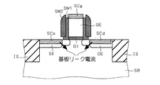
また、Nチャネル型MISFETにおいて、シリサイド化しようとする領域への予めのフッ素注入を行う場合であっても、MISFETの構造によっては、ドレイン−ボディ間オフリーク電流Ioffbが上昇してしまう場合がある。図16〜図18は、ドレイン−ボディ間オフリーク電流(基板リーク電流)Ioffbが劣化する場合のMISFET製造工程を示す図である。 Further, in the N-channel MISFET, even if fluorine is previously implanted into the region to be silicided, the drain-body off-leakage current Ioffb may increase depending on the structure of the MISFET. 16 to 18 are diagrams showing a MISFET manufacturing process when the drain-body off-leak current (substrate leak current) Ioffb deteriorates.
図16に示すように、半導体基板SB上に形成されたサイドウォール絶縁膜SW1,SW2のうち、サイドウォール絶縁膜SW1はTEOS(テトラエトキシシラン)酸化膜で、サイドウォール絶縁膜SW2はシリコン窒化膜で、それぞれ形成されることが多い。この構造の場合、シリサイド化直前に、シリサイド化領域表面付近をフッ酸等で洗浄(軽いウェットエッチング)すると、TEOS酸化膜がエッチングされてしまい、サイドウォール絶縁膜SW1の露出部AR1,AR2に後退が見られやすい。 As shown in FIG. 16, of the sidewall insulating films SW1 and SW2 formed on the semiconductor substrate SB, the sidewall insulating film SW1 is a TEOS (tetraethoxysilane) oxide film, and the sidewall insulating film SW2 is a silicon nitride film. In many cases, each is formed. In this structure, if the vicinity of the silicidation region surface is cleaned with hydrofluoric acid or the like (light wet etching) immediately before silicidation, the TEOS oxide film is etched and recedes to the exposed portions AR1 and AR2 of the sidewall insulating film SW1. Is easy to see.
この後、図17に示すように、全面にNi等の金属膜MTを形成し、シリサイド化を行って、第1アニール処理、未反応部分の金属膜MTの除去、および、第2アニール処理を行えば、図18に示すようにシリサイド化領域SCs,SCdが形成される。このとき、図17に示すように、後退した露出部AR2に金属膜MTが回り込んで形成されるため、シリサイド領域SCs,SCdはよりチャネルの近くにまで形成されることとなる。 Thereafter, as shown in FIG. 17, a metal film MT of Ni or the like is formed on the entire surface, silicidation is performed, and the first annealing process, the removal of the unreacted portion of the metal film MT, and the second annealing process are performed. In this case, silicidation regions SCs and SCd are formed as shown in FIG. At this time, as shown in FIG. 17, since the metal film MT is formed around the recessed exposed portion AR2, the silicide regions SCs and SCd are formed closer to the channel.
これにより、ドレイン−ボディ間オフリーク電流Ioffbは、露出部AR2の後退量が増えるほど大きな値になってしまう。よって、図18のような構造であれば、Nチャネル型MISFETにおいて、シリサイド化しようとする領域へ予めフッ素注入を行ったとしても、リーク電流抑制の効果が薄れてしまうこととなる。 As a result, the drain-body off-leakage current Ioffb becomes larger as the retraction amount of the exposed portion AR2 increases. Therefore, with the structure as shown in FIG. 18, even if fluorine is previously implanted into the region to be silicided in the N channel MISFET, the effect of suppressing the leakage current is diminished.
本発明に係る実施の形態は、マスク層によりPチャネル型MISFETを覆いつつ、Nチャネル型MISFETのN型ソース領域およびN型ドレイン領域にイオンを注入し、その後、Nチャネル型MISFETおよびPチャネル型MISFETの各ゲート電極、ソース領域およびドレイン領域にシリサイド化を行う、半導体装置およびその製造方法である。 In the embodiment of the present invention, ions are implanted into the N-type source region and the N-type drain region of the N-channel MISFET while covering the P-channel MISFET with the mask layer, and then the N-channel MISFET and the P-channel type. A semiconductor device and a manufacturing method thereof for siliciding each gate electrode, source region, and drain region of a MISFET.
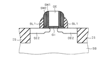
図1および図2は、本発明を適用可能な半導体装置の断面図および上面図である。なお図1は、図2中の切断線I−Iにおける断面図である。図2では、ゲート電極GE、ソース領域SEおよびドレイン領域DEを有する各MISFET(Metal Insulator Semiconductor Field Effect Transistor)が、シリコン酸化膜等の素子分離膜ISにより分離された半導体装置が示されている。 1 and 2 are a cross-sectional view and a top view of a semiconductor device to which the present invention can be applied. 1 is a cross-sectional view taken along a cutting line II in FIG. FIG. 2 shows a semiconductor device in which each MISFET (Metal Insulator Semiconductor Field Effect Transistor) having a gate electrode GE, a source region SE, and a drain region DE is separated by an element isolation film IS such as a silicon oxide film.
図1に示されているように、この半導体装置は、シリコン基板等の半導体基板SBと、ゲート絶縁膜(例えばシリコン酸化膜)GIおよびゲート電極(例えばポリシリコン膜)GEの積層構造、ソース領域SE、ドレイン領域DEを含む、半導体基板SB上に形成されたMISFETとを備える。なお、ソース領域SEおよびドレイン領域DEの外側には素子分離膜ISが形成されている。 As shown in FIG. 1, the semiconductor device includes a semiconductor substrate SB such as a silicon substrate, a stacked structure of a gate insulating film (for example, silicon oxide film) GI and a gate electrode (for example, polysilicon film) GE, and a source region. SE and MISFET formed on semiconductor substrate SB including drain region DE are provided. An element isolation film IS is formed outside the source region SE and the drain region DE.
ゲート電極GE、ソース領域SEおよびドレイン領域DEの各表面には、Ni(ニッケル)やCo(コバルト)等を含むシリサイド化領域SCg,SCs,SCdが、それぞれ形成されている。なお、ゲート絶縁膜GIおよびゲート電極GEの積層構造の側面、並びに、ソース領域SEおよびドレイン領域DEの表面の一部に面して、それぞれTEOS酸化膜等の第1サイドウォール絶縁膜SW1が形成されている。また、第1サイドウォール絶縁膜SW1を介しつつ、ゲート絶縁膜GIおよびゲート電極GEの積層構造の側面、並びに、ソース領域SEおよびドレイン領域DEの表面の一部に対向して、それぞれシリコン窒化膜等の第2サイドウォール絶縁膜SW2が形成されている。 Silicided regions SCg, SCs, and SCd containing Ni (nickel), Co (cobalt), and the like are formed on the surfaces of the gate electrode GE, the source region SE, and the drain region DE, respectively. A first sidewall insulating film SW1 such as a TEOS oxide film is formed on the side surface of the stacked structure of the gate insulating film GI and the gate electrode GE and on part of the surface of the source region SE and the drain region DE. Has been. In addition, the silicon nitride film faces the side surface of the stacked structure of the gate insulating film GI and the gate electrode GE and part of the surface of the source region SE and the drain region DE through the first sidewall insulating film SW1. A second sidewall insulating film SW2 is formed.
なお、図2に示した半導体装置はCMOS構造を有しており、Nチャネル型MISFETおよびPチャネル型MISFETの両者を備える。そして、図1に示すMISFETの構造は、Nチャネル型MISFETおよびPチャネル型MISFETに共通しており、両チャネル型MISFETは、半導体基板SBに形成されたウェル(図示せず)、ソース領域SE、ドレイン領域DEの各領域における導電型が異なる以外は、同一構造を有する。また、図1においては、ドレイン−ボディ間オフリーク電流(基板リーク電流)を符号Ioffbとして示している。 Note that the semiconductor device shown in FIG. 2 has a CMOS structure and includes both an N-channel MISFET and a P-channel MISFET. The structure of the MISFET shown in FIG. 1 is common to the N-channel MISFET and the P-channel MISFET, and both the channel MISFETs include a well (not shown) formed in the semiconductor substrate SB, a source region SE, The drain region DE has the same structure except that the conductivity type in each region is different. In FIG. 1, the drain-body off-leakage current (substrate leakage current) is indicated by a symbol Ioffb.
図3〜図9は、本発明の実施の形態に係る半導体装置の製造方法の各工程を示す図である。以下、各図を用いて本発明の実施の形態に係る半導体装置の製造方法を説明する。 3 to 9 are diagrams showing each step of the manufacturing method of the semiconductor device according to the embodiment of the present invention. A method for manufacturing a semiconductor device according to an embodiment of the present invention will be described below with reference to the drawings.
まず、図3に示すように、半導体基板SB上に、ゲート絶縁膜GIおよびゲート電極GEの積層構造、第1サイドウォール絶縁膜SW1、第2サイドウォール絶縁膜SW2、ソース領域のLDD(Lightly Doped Drain)領域SE1、並びに、ドレイン領域のLDD領域DE1を含むMISFETを、Pチャネル型およびNチャネル型のそれぞれにつき、フォトリソグラフィ技術およびエッチング技術、イオン注入技術等を用いて形成する。 First, as shown in FIG. 3, on the semiconductor substrate SB, a stacked structure of the gate insulating film GI and the gate electrode GE, the first sidewall insulating film SW1, the second sidewall insulating film SW2, and the LDD (Lightly Doped) of the source region. The MISFET including the drain region SE1 and the drain region LDD region DE1 is formed by using a photolithography technique, an etching technique, an ion implantation technique, and the like for each of the P channel type and the N channel type.
次に、図4に示すように、イオン注入IP1を行って、ソース領域SE2およびドレイン領域DE2の形成を行う。なお、N型ソース領域およびN型ドレイン領域の形成に当たっては、例えばAs(砒素)イオンを5〜50[keV]および1×10¹⁵〜1×10¹⁶[cm-2]の条件下で半導体基板SBに注入することにより形成すればよい。また、P型ソース領域およびP型ドレイン領域の形成に当たっては、例えばB(ボロン)イオンを1〜5[keV]および1×10¹⁵〜1×10¹⁶[cm-2]の条件下で半導体基板SBに注入することにより形成すればよい。もちろん、本発明に係る半導体装置はCMOS構造を有するので、フォトレジストをマスクとして用いることにより、Nチャネル型MISFETのソース・ドレイン形成用のイオン注入と、Pチャネル型のソース・ドレイン形成用のイオン注入とを、選択的に打ち分ければよい。 Next, as shown in FIG. 4, ion implantation IP1 is performed to form the source region SE2 and the drain region DE2. In forming the N-type source region and the N-type drain region, for example, As (arsenic) ions are used under the conditions of 5 to 50 [keV] and 1 × 10 15 to 1 × 10 16 [cm −2 ]. What is necessary is just to form by inject | pouring into SB. In forming the P-type source region and the P-type drain region, for example, B (boron) ions are applied under the conditions of 1 to 5 [keV] and 1 × 10 15 to 1 × 10 16 [cm −2 ]. What is necessary is just to form by inject | pouring into SB. Of course, since the semiconductor device according to the present invention has a CMOS structure, by using a photoresist as a mask, ion implantation for forming a source / drain of an N-channel MISFET and ions for forming a P-channel source / drain are performed. The injection may be selectively divided.
次に、図5に示すように、半導体基板SBのうちシリサイド化を防止すべき部分を覆うためのシリサイド化防止膜BLを、Pチャネル型MISFET、Nチャネル型MISFETおよび半導体基板SBの表面を覆うように形成する。このシリサイド化防止膜BLとしては、CVD(Chemical Vapor Deposition)法により成膜温度400度で形成したUSG(Undoped Silicate Glass)膜を採用すればよい。 Next, as shown in FIG. 5, an anti-silicidation film BL for covering a portion of the semiconductor substrate SB that should be prevented from silicidization covers the surfaces of the P-channel MISFET, the N-channel MISFET, and the semiconductor substrate SB. To form. As this silicidation preventing film BL, a USG (Undoped Silicate Glass) film formed by a CVD (Chemical Vapor Deposition) method at a film forming temperature of 400 ° C. may be employed.
そして、フォトリソグラフィ技術およびエッチング技術を用いて、シリサイド化防止膜BLに対して選択的に異方性エッチング(ドライエッチング)を行い、シリサイド化を防止すべき部分(例えば配線のコンタクト領域等のうちシリサイド化したくない部分(図示せず)など)、および、Pチャネル型MISFETのゲート絶縁膜GIおよびゲート電極GEの積層構造の側方、および、Nチャネル型MISFETのゲート絶縁膜GIおよびゲート電極GEの積層構造の側方に、シリサイド化防止膜BL1を残置する(図6)。 Then, anisotropic etching (dry etching) is selectively performed on the silicidation preventing film BL by using a photolithography technique and an etching technique, and a portion where the silicidation is to be prevented (for example, a contact region of the wiring) A portion (not shown) that is not desired to be silicided, the side of the stacked structure of the gate insulating film GI and the gate electrode GE of the P-channel type MISFET, and the gate insulating film GI and the gate electrode GE of the N-channel type MISFET An anti-silicidation film BL1 is left on the side of the stacked structure (FIG. 6).
次に、図7に示すように、Nチャネル型MISFETは覆わずに、Pチャネル型MISFETを選択的に覆うマスク層RMを形成する。マスク層RMにはフォトレジストを採用し、このフォトレジストをパターニングすればよい。そして、マスク層RMによりPチャネル型MISFETを覆いつつ、Nチャネル型MISFETの少なくともN型ソース領域およびN型ドレイン領域に、フッ素イオン(“F+”と表示)および/またはシリコンイオン(“Si+”と表示)の注入IP2を行う。なお、このイオン注入IP2は、フッ素イオン及びシリコンイオンいずれの場合も、5[keV]および6×1014〜1×1015[cm-2]程度の条件下で行えばよい。 Next, as shown in FIG. 7, a mask layer RM that selectively covers the P-channel MISFET without forming the N-channel MISFET is formed. A photoresist is employed for the mask layer RM, and this photoresist may be patterned. Then, while covering the P-channel MISFET with the mask layer RM, at least the N-type source region and the N-type drain region of the N-channel MISFET have fluorine ions (indicated as “F + ”) and / or silicon ions (“Si + ”). Injection IP2 is performed. The ion implantation IP2 may be performed under conditions of about 5 [keV] and about 6 × 10 14 to 1 × 10 15 [cm −2 ] in both cases of fluorine ions and silicon ions.
また、このイオン注入IP2は、フッ素イオン及びシリコンイオンに限らず、フッ素、シリコン、C(炭素)、Ge(ゲルマニウム)、Ne(ネオン)、Ar(アルゴン)、Kr(クリプトン)のうち少なくとも一種類を含むイオンを注入することにより行なってもよい。 The ion implantation IP2 is not limited to fluorine ions and silicon ions, but is at least one of fluorine, silicon, C (carbon), Ge (germanium), Ne (neon), Ar (argon), and Kr (krypton). It may be performed by implanting ions containing.
次に、半導体基板SB表面やゲート電極GE表面に生じたシリコン酸化膜を除去するための、シリサイド化を行う部分の洗浄を行う。この洗浄工程においては、RCA洗浄に加えてフッ酸を用いた洗浄を行えばよい。また、その他にも、前洗浄(ケミカルドライクリーニング)装置とスパッタ装置とが一体化された装置の前洗浄であってもよい。 Next, in order to remove the silicon oxide film generated on the surface of the semiconductor substrate SB and the surface of the gate electrode GE, a portion to be silicided is cleaned. In this cleaning step, cleaning using hydrofluoric acid may be performed in addition to RCA cleaning. In addition, pre-cleaning of an apparatus in which a pre-cleaning (chemical dry cleaning) apparatus and a sputtering apparatus are integrated may be used.
なおこのとき、残置したシリサイド化防止膜BL1とシリサイド化を行う部分とに対して、洗浄を行う。この洗浄により、Pチャネル型MISFETのゲート絶縁膜GIおよびゲート電極GEの積層構造の側方、および、Nチャネル型MISFETのゲート絶縁膜GIおよびゲート電極GEの積層構造の側方に残置したシリサイド化防止膜BL1は除去される。一方、それ以外の部分のシリサイド化防止膜BL1(図示せず)は、この洗浄では完全には除去されず、残置したままとなる。 At this time, the remaining silicidation preventing film BL1 and the portion to be silicidized are cleaned. By this cleaning, silicidation left on the side of the stacked structure of the gate insulating film GI and the gate electrode GE of the P-channel MISFET and on the side of the stacked structure of the gate insulating film GI and the gate electrode GE of the N-channel MISFET. The prevention film BL1 is removed. On the other hand, the silicidation preventing film BL1 (not shown) in the other portions is not completely removed by this cleaning, and remains as it is.
次に、Nチャネル型MISFET、Pチャネル型MISFET、半導体基板SBの表面、および、残置したシリサイド化防止膜BL1上に、Ni等の金属膜MTをスパッタ法等により図8に示すように形成する。そして、一回目のRTA(Rapid Thermal Annealing)を行い、その後、未反応の金属膜を除去して、二回目のRTAを行う。これにより、Nチャネル型MISFETのゲート電極、イオン注入されたN型ソース領域およびN型ドレイン領域、並びに、Pチャネル型MISFETのゲート電極、P型ソース領域およびP型ドレイン領域に、それぞれシリサイド化が行われ、図9に示すように、ゲート電極GE、ソース領域SEおよびドレイン領域DEの各表面に、シリサイド化領域SCg,SCs,SCdが、それぞれ形成される。 Next, a metal film MT such as Ni is formed by sputtering or the like on the surface of the N channel MISFET, P channel MISFET, semiconductor substrate SB, and the remaining silicidation prevention film BL1 as shown in FIG. . Then, the first RTA (Rapid Thermal Annealing) is performed, and then the unreacted metal film is removed and the second RTA is performed. As a result, silicidation occurs in the gate electrode of the N-channel type MISFET, the N-type source region and N-type drain region into which ions are implanted, and the gate electrode, P-type source region and P-type drain region of the P-channel type MISFET. As shown in FIG. 9, silicided regions SCg, SCs, and SCd are formed on the surfaces of the gate electrode GE, the source region SE, and the drain region DE, respectively.
なお、金属膜MTにはNi以外にも、Ni、Ti(チタン)、Co(コバルト)、Pd(パラジウム)、Pt(白金)、Er(エルビウム)のうち少なくとも一種類を含む金属膜を採用してもよい。 In addition to Ni, the metal film MT employs a metal film including at least one of Ni, Ti (titanium), Co (cobalt), Pd (palladium), Pt (platinum), and Er (erbium). May be.
上記非特許文献1においては、シリサイド化しようとする領域に予めフッ素をイオン注入すればリーク電流を抑制可能と報告されていたが、本願発明者らは、フッ素イオンだけではなく、フッ素、シリコン、炭素、ゲルマニウム、ネオン、アルゴン、クリプトンのうち少なくとも一種類を含むイオンをNチャネル型MISFETのN型ソース領域およびN型ドレイン領域に注入する場合であっても、同様にリーク電流を抑制可能なことを発見した。
In the
図10は、フッ素注入またはシリコン注入を予め行った上でN型ソース領域およびN型ドレイン領域をNiシリサイド化した多数のNチャネル型MISFETにつき、ドレイン−ボディ間オフリーク電流(基板リーク電流)Ioffbの計測を行った結果の例を示すグラフである。 FIG. 10 shows drain-body off-leakage current (substrate leakage current) Ioffb for a number of N-channel MISFETs in which N-type source regions and N-type drain regions are Ni-silicided after fluorine implantation or silicon implantation has been performed in advance. It is a graph which shows the example of the result of having measured.
図10において、縦軸は、全Nチャネル型MISFETの正規分布計測結果における分位点(値“0”が最頻値)を示し、横軸は基板リーク電流値(任意単位)を示している。また、“F,Si注入”と示した計測結果は、5[keV]および1×10¹⁵[cm-2]の条件下でフッ素注入を行った上でN型ソース領域およびN型ドレイン領域をNiシリサイド化した結果、5[keV]および6×10¹⁴[cm-2]の条件下でフッ素注入を行った上でN型ソース領域およびN型ドレイン領域をNiシリサイド化した結果、5[keV]および1×10¹⁵[cm-2]の条件下でシリコン注入を行った上でN型ソース領域およびN型ドレイン領域をNiシリサイド化した結果、および、5[keV]および6×10¹⁴[cm-2]の条件下でシリコン注入を行った上でN型ソース領域およびN型ドレイン領域をNiシリサイド化した結果をそれぞれ示し、“Reference”と示した計測結果はフッ素注入を行わずにN型ソース領域およびN型ドレイン領域をNiシリサイド化した場合の参照値を示している。 In FIG. 10, the vertical axis represents the quantile (value “0” is the mode value) in the normal distribution measurement result of all N-channel MISFETs, and the horizontal axis represents the substrate leakage current value (arbitrary unit). . In addition, the measurement result shown as “F, Si implantation” shows that the N-type source region and the N-type drain region are formed after fluorine implantation is performed under conditions of 5 [keV] and 1 × 10 15 [cm −2 ]. As a result of Ni silicidation, fluorine implantation was performed under the conditions of 5 [keV] and 6 × 10 14 [cm −2 ], and then the N-type source region and N-type drain region were Ni-silicided. ] And 1 × 10 15 [cm −2 ] after silicon implantation, the N-type source region and the N-type drain region were Ni-silicided, and 5 [keV] and 6 × 10 14 [ cm −2 ] shows the result of Ni-silicidation of the N-type source region and N-type drain region after silicon implantation, and the measurement result indicated as “Reference” indicates that N was not implanted with fluorine. Type source area The reference value when the region and the N-type drain region are Ni-silicided is shown.
図10から分かるように、ドレイン−ボディ間オフリーク電流(基板リーク電流)Ioffbの値は、フッ素注入を行わずにソース領域およびドレイン領域をNiシリサイド化した場合(“Reference”)よりも、フッ素またはシリコンの注入を行った上でN型ソース領域およびN型ドレイン領域をNiシリサイド化した場合の方が低い。 As can be seen from FIG. 10, the value of the drain-body off-leakage current (substrate leakage current) Ioffb is higher than that in the case where the source region and the drain region are Ni-silicided (“Reference”) without fluorine implantation. It is lower when the N-type source region and the N-type drain region are Ni-silicided after silicon implantation.
一方、本願では、シリサイド化しようとする領域への予めのフッ素注入がリーク電流抑制に逆効果となるPチャネル型MISFETには、マスクRMを形成する。これにより、シリサイド化しようとする領域への予めのフッ素やシリコン等のイオン注入は行わない。 On the other hand, in the present application, a mask RM is formed in a P-channel type MISFET in which fluorine injection into a region to be silicided has an adverse effect on leakage current suppression. Thereby, ion implantation of fluorine, silicon, or the like in advance into the region to be silicided is not performed.
すなわち、本発明によれば、マスク層RMによりPチャネル型MISFETを覆いつつ、Nチャネル型MISFETのN型ソース領域およびN型ドレイン領域にイオンを注入する。その後、Nチャネル型MISFETおよびPチャネル型MISFETの各ゲート電極、ソース領域およびドレイン領域にシリサイド化を行う。言い換えれば、本願ではPチャネル型MISFETのP型ソース領域およびP型ドレイン領域にはイオンを注入することなく、かつ、Nチャネル型MISFETのN型ソース領域およびN型ドレイン領域にはイオンを注入した後に、シリサイド化を行うことができる。これにより、Pチャネル型MISFETにおいてドレイン−ボディ間オフリーク電流Ioffbを劣化させること無く、Nチャネル型MISFETにおいてドレイン−ボディ間オフリーク電流(基板リーク電流)Ioffbの抑制が図れる。よって、より確実にMISFETにおけるリーク電流の抑制が図れる半導体装置の製造方法が実現できる。 That is, according to the present invention, ions are implanted into the N-type source region and the N-type drain region of the N-channel MISFET while covering the P-channel MISFET with the mask layer RM. Thereafter, silicidation is performed on each gate electrode, source region, and drain region of the N-channel type MISFET and the P-channel type MISFET. In other words, in this application, ions are not implanted into the P-type source region and the P-type drain region of the P-channel type MISFET, and ions are implanted into the N-type source region and the N-type drain region of the N-channel type MISFET. Later, silicidation can be performed. As a result, the drain-body off-leakage current (substrate leakage current) Ioffb can be suppressed in the N-channel MISFET without degrading the drain-body off-leakage current Ioffb in the P-channel MISFET. Therefore, it is possible to realize a method for manufacturing a semiconductor device that can more reliably suppress the leakage current in the MISFET.
また、本発明によれば、Pチャネル型MISFETのゲート絶縁膜GIおよびゲート電極GEの積層構造の側方、および、Nチャネル型MISFETのゲート絶縁膜GIおよびゲート電極GEの積層構造の側方にシリサイド化防止膜BL1を残置し、残置したシリサイド化防止膜BL1とシリサイド化を行う部分とに対して、洗浄を行う。シリサイド化防止膜BL1がゲート絶縁膜GIおよびゲート電極GEの積層構造の側方に残置しているので、シリサイド化を行う部分の洗浄時に、Nチャネル型MISFETのゲート絶縁膜GIおよびゲート電極GEの積層構造およびPチャネル型MISFETのゲート絶縁膜GIおよびゲート電極GEの積層構造に付随するサイドウォール絶縁膜SW1,SW2部分のエッチングがされにくい。よって、Nチャネル型MISFETおよびPチャネル型MISFETの各ソース領域および各ドレイン領域におけるシリサイド化領域が、チャネル近くにまで入り込みにくく、より確実にMISFETにおけるリーク電流の抑制が図れる半導体装置の製造方法が実現できる。 Further, according to the present invention, the side of the stacked structure of the gate insulating film GI and the gate electrode GE of the P-channel MISFET and the side of the stacked structure of the gate insulating film GI and the gate electrode GE of the N-channel MISFET. The silicidation prevention film BL1 is left, and the remaining silicidation prevention film BL1 and the portion to be silicided are cleaned. Since the silicidation preventing film BL1 is left on the side of the laminated structure of the gate insulating film GI and the gate electrode GE, when the portion to be silicidized is cleaned, the gate insulating film GI and the gate electrode GE of the N channel MISFET Etching of the side wall insulating films SW1 and SW2 accompanying the laminated structure and the laminated structure of the gate insulating film GI and the gate electrode GE of the P-channel type MISFET is difficult. Accordingly, a method for manufacturing a semiconductor device is realized in which the silicide regions in the source region and the drain region of the N channel MISFET and the P channel MISFET do not easily enter the vicinity of the channel, and the leakage current in the MISFET can be more reliably suppressed. it can.
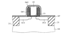
図11は、洗浄後の本発明に係る半導体装置の構造を示す断面図である。図11においては、右側にNチャネル型MISFETが、左側にPチャネル型MISFETが、それぞれ示されている。図11の構造のうちNチャネル型MISFETにおいては、半導体基板SBの表面からの第1サイドウォール絶縁膜SW1の高さは、半導体基板SBの表面からの第2サイドウォール絶縁膜SW2の高さよりも小さい。また、Nチャネル型MISFETにおいては、ゲート絶縁膜GIおよびゲート電極GEの積層構造の側面からの第1サイドウォール絶縁膜SW1の最大距離は、ゲート絶縁膜GIおよびゲート電極GEの積層構造の側面からの第2サイドウォール絶縁膜SW2の最大距離よりも小さい。そして、第2サイドウォール絶縁膜SW2のゲート側面からの最大距離と第1サイドウォール絶縁膜SW1のゲート側面からの最大距離との差Bnは、第1サイドウォール絶縁膜SW1の高さと第2サイドウォール絶縁膜SW2の高さとの差Anよりも小さい。 FIG. 11 is a cross-sectional view showing the structure of the semiconductor device according to the present invention after cleaning. In FIG. 11, an N-channel MISFET is shown on the right side, and a P-channel MISFET is shown on the left side. In the N-channel MISFET of the structure of FIG. 11, the height of the first sidewall insulating film SW1 from the surface of the semiconductor substrate SB is higher than the height of the second sidewall insulating film SW2 from the surface of the semiconductor substrate SB. small. In the N channel MISFET, the maximum distance of the first sidewall insulating film SW1 from the side surface of the stacked structure of the gate insulating film GI and the gate electrode GE is from the side surface of the stacked structure of the gate insulating film GI and the gate electrode GE. This is smaller than the maximum distance of the second sidewall insulating film SW2. The difference Bn between the maximum distance from the gate side surface of the second sidewall insulating film SW2 and the maximum distance from the gate side surface of the first sidewall insulating film SW1 is the height of the first sidewall insulating film SW1 and the second side. It is smaller than the difference An from the height of the wall insulating film SW2.
なお、図12は、イオン注入がない場合の、洗浄後のNチャネル型MISFETの構造を示す断面図である。図12においては、第2サイドウォール絶縁膜SW2のゲート側面からの最大距離と第1サイドウォール絶縁膜SW1のゲート側面からの最大距離との差Bn1は、第1サイドウォール絶縁膜SW1の高さと第2サイドウォール絶縁膜SW2の高さとの差An1と同程度である。 FIG. 12 is a cross-sectional view showing the structure of the N-channel MISFET after cleaning when no ion implantation is performed. In FIG. 12, the difference Bn1 between the maximum distance from the gate side surface of the second sidewall insulating film SW2 and the maximum distance from the gate side surface of the first sidewall insulating film SW1 is the height of the first sidewall insulating film SW1. The difference An1 from the height of the second sidewall insulating film SW2 is approximately the same.
本願発明者らは、図11のBnと図12のBn1との大きさの違いについて下記のように考える。 The inventors consider the difference in size between Bn in FIG. 11 and Bn1 in FIG. 12 as follows.
すなわち、フッ素やシリコン等のイオン注入が行われる図11の場合、第1サイドウォール絶縁膜SW1のゲート電極GEの側面に接触する部分の頂部には、イオンが比較的多く注入される。一方、第1サイドウォール絶縁膜SW1のソース領域SEおよびドレイン領域DEに接触する部分の端部上には、第2サイドウォール絶縁膜SW2が存在し、さらに、その側方にはシリサイド化防止膜BL1が残置する。 That is, in the case of FIG. 11 where ion implantation of fluorine, silicon, or the like is performed, a relatively large amount of ions are implanted into the top of the portion of the first sidewall insulating film SW1 that contacts the side surface of the gate electrode GE. On the other hand, the second sidewall insulating film SW2 is present on the end portion of the first sidewall insulating film SW1 that is in contact with the source region SE and the drain region DE. BL1 remains.
このため、本発明においては、第1サイドウォール絶縁膜SW1のソース領域SEおよびドレイン領域DEに接触する部分の端部付近よりも、ゲート電極GEの側面に接触する部分の頂部付近に、より多くのイオンが注入されることとなる。 For this reason, in the present invention, more in the vicinity of the top of the portion in contact with the side surface of the gate electrode GE than in the vicinity of the end of the portion in contact with the source region SE and drain region DE of the first sidewall insulating film SW1. Ions are implanted.
図13のグラフに示すように、第1サイドウォール絶縁膜SW1を構成するTEOS酸化膜も、第2サイドウォール絶縁膜SW2を構成するシリコン窒化膜も、イオンが注入されると、そのドーズ量が多くなるにつれてシリサイド化工程直前の洗浄時にエッチングされる量が多くなることが分かっている。 As shown in the graph of FIG. 13, when ions are implanted into the TEOS oxide film constituting the first sidewall insulating film SW1 and the silicon nitride film constituting the second sidewall insulating film SW2, the dose amount is increased. It has been found that as the amount increases, the amount etched during cleaning immediately before the silicidation step increases.
よって、本発明に係る半導体装置の製造方法を用いて、Nチャネル型MISFETにイオン注入の工程を行い、洗浄工程、シリサイド化工程を行うと、シリサイド化工程直前の洗浄時に、第1サイドウォール絶縁膜SW1のゲート電極GEの側面に接触する部分の頂部付近が比較的多くエッチングされ、一方、第1サイドウォール絶縁膜SW1のソース領域SEおよびドレイン領域DEに接触する部分の端部付近は比較的少なくエッチングされるのである。これが、第2サイドウォール絶縁膜SW2のゲート側面からの最大距離と第1サイドウォール絶縁膜SW1のゲート側面からの最大距離との差Bnは、第1サイドウォール絶縁膜SW1の高さと第2サイドウォール絶縁膜SW2の高さとの差Anよりも小さい理由と考えられる。 Therefore, when the ion implantation process is performed on the N-channel MISFET and the cleaning process and the silicidation process are performed using the semiconductor device manufacturing method according to the present invention, the first sidewall insulation is performed at the time of cleaning immediately before the silicidation process. The vicinity of the top of the portion of the film SW1 in contact with the side surface of the gate electrode GE is etched much, while the vicinity of the end of the portion of the first sidewall insulating film SW1 in contact with the source region SE and drain region DE is relatively It is etched a little. This is because the difference Bn between the maximum distance from the gate side surface of the second sidewall insulating film SW2 and the maximum distance from the gate side surface of the first sidewall insulating film SW1 is the height of the first sidewall insulating film SW1 and the second side. The reason is considered to be smaller than the difference An from the height of the wall insulating film SW2.
一方、イオン注入工程を行わない場合には、シリサイド化工程直前の洗浄時の、第1サイドウォール絶縁膜SW1のゲート電極GEの側面に接触する部分の頂部付近のエッチング量と、第1サイドウォール絶縁膜SW1のソース領域SEおよびドレイン領域DEに接触する部分の端部付近のエッチング量との間に差は生じない。これが、第2サイドウォール絶縁膜SW2のゲート側面からの最大距離と第1サイドウォール絶縁膜SW1のゲート側面からの最大距離との差Bn1は、第1サイドウォール絶縁膜SW1の高さと第2サイドウォール絶縁膜SW2の高さとの差An1と同程度である理由と考えられる。 On the other hand, when the ion implantation step is not performed, the etching amount near the top of the portion of the first sidewall insulating film SW1 that contacts the side surface of the gate electrode GE at the time of cleaning immediately before the silicidation step, and the first sidewall There is no difference between the etching amount in the vicinity of the end portion of the insulating film SW1 in contact with the source region SE and the drain region DE. This is because the difference Bn1 between the maximum distance from the gate side surface of the second sidewall insulating film SW2 and the maximum distance from the gate side surface of the first sidewall insulating film SW1 is the height of the first sidewall insulating film SW1 and the second side. This is probably because the difference An1 from the height of the wall insulating film SW2 is approximately the same.
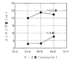
図14は、フッ素注入を予め行った上でゲート電極GEのシリサイド化を行った多数のNチャネル型MISFETにつき、ゲート電極GEのシート抵抗の計測を行った結果を示すグラフである。図14において、縦軸は、全Nチャネル型MISFETの正規分布計測結果における分位点(値“0”が最頻値)を示し、横軸はシート抵抗値(任意単位)を示している。また、“F注入”と示したグラフは5[keV]および1×10¹⁵[cm-2]の条件下でフッ素注入を行った上でゲート電極GEをNiシリサイド化した結果、および、5[keV]および6×10¹⁴[cm-2]の条件下でフッ素注入を行った上でゲート電極GEをNiシリサイド化した結果を示し、“Reference”と示したグラフはフッ素注入を行わずにゲート電極GEをNiシリサイド化した場合の参照値を示している。フッ素注入を予め行った上でゲート電極GEのシリサイド化を行ったNチャネル型MISFETの方が、シート抵抗値が低くなっていることが分かる。 FIG. 14 is a graph showing the result of measuring the sheet resistance of the gate electrode GE for a number of N-channel MISFETs in which the gate electrode GE was silicidized after fluorine implantation was performed in advance. In FIG. 14, the vertical axis represents the quantile (value “0” is the mode value) in the normal distribution measurement result of all N-channel MISFETs, and the horizontal axis represents the sheet resistance value (arbitrary unit). Further, the graph indicated as “F implantation” shows the result of Ni silicide formation of the gate electrode GE after performing fluorine implantation under conditions of 5 [keV] and 1 × 10 15 [cm −2 ], and 5 [ The result is that the gate electrode GE was Ni-silicided after fluorine implantation under the conditions of keV] and 6 × 10 14 [cm −2 ], and the graph labeled “Reference” shows the gate without fluorine implantation. Reference values when the electrode GE is Ni-silicided are shown. It can be seen that the sheet resistance value is lower in the N-channel MISFET in which the gate electrode GE is silicided after the fluorine implantation is performed in advance.
なお、Pチャネル型MISFETにおいてはイオン注入が行われないことから、シリサイド化工程直前の洗浄時には、Pチャネル型MISFETの第1サイドウォール絶縁膜SW1の頂部付近のエッチング量は、Nチャネル型MISFETの第1サイドウォール絶縁膜SW1の頂部付近のエッチング量よりも大幅に少なくなる。図11の左側においては、Pチャネル型MISFETの第1サイドウォール絶縁膜SW1の高さの方が、第2サイドウォール絶縁膜SW2の高さよりも大きく、その差をApとして示している。 Since no ion implantation is performed in the P-channel type MISFET, the etching amount near the top of the first sidewall insulating film SW1 of the P-channel type MISFET is equal to that of the N-channel type MISFET during cleaning immediately before the silicidation process. The amount of etching near the top of the first sidewall insulating film SW1 is significantly smaller. On the left side of FIG. 11, the height of the first sidewall insulating film SW1 of the P-channel type MISFET is larger than the height of the second sidewall insulating film SW2, and the difference is shown as Ap.
そして、Pチャネル型MISFETにおいてもNチャネル型MISFETの場合と同様、ゲート絶縁膜GIおよびゲート電極GEの積層構造の側面からの第1サイドウォール絶縁膜SW1の最大距離は、ゲート絶縁膜GIおよびゲート電極GEの積層構造の側面からの第2サイドウォール絶縁膜SW2の最大距離よりも小さいが、Pチャネル型MISFETにおける第2サイドウォール絶縁膜SW2のゲート側面からの最大距離と第1サイドウォール絶縁膜SW1のゲート側面からの最大距離との差Bpは、Nチャネル型MISFETの第2サイドウォール絶縁膜SW2のゲート側面からの最大距離と第1サイドウォール絶縁膜SW1のゲート側面からの最大距離との差Bnに、略等しい。 In the P-channel type MISFET, as in the case of the N-channel type MISFET, the maximum distance of the first sidewall insulating film SW1 from the side surface of the stacked structure of the gate insulating film GI and the gate electrode GE is equal to the gate insulating film GI and the gate. Although it is smaller than the maximum distance of the second sidewall insulating film SW2 from the side surface of the stacked structure of the electrode GE, the maximum distance from the gate side surface of the second sidewall insulating film SW2 in the P-channel MISFET and the first sidewall insulating film The difference Bp between the maximum distance from the gate side surface of SW1 is the maximum distance from the gate side surface of the second sidewall insulating film SW2 of the N-channel MISFET and the maximum distance from the gate side surface of the first sidewall insulating film SW1. It is substantially equal to the difference Bn.
このように、本発明の半導体装置の構造によれば、Nチャネル型MISFETにおいて、第2サイドウォール絶縁膜SW2のゲート側面からの最大距離と第1サイドウォール絶縁膜SW1のゲート側面からの最大距離との差Bnは、第1サイドウォール絶縁膜SW1の高さと第2サイドウォール絶縁膜SW2の高さとの差Anよりも小さい。よって、シリサイド化を行う際に、N型ソース領域およびN型ドレイン領域におけるシリサイド化領域が、チャネル近くにまで入り込みにくく、より確実にMISFETにおけるリーク電流の抑制が図れる半導体装置が実現できる。また、第1サイドウォール絶縁膜SW1の高さは、第2サイドウォール絶縁膜SW2の高さよりも小さい。よって、ゲート電極GEにシリサイド化を行うと、第2サイドウォール絶縁膜SW2の高さよりも低い部分にまで入り込んでゲート電極GEがシリサイド化され、ゲート電極GEの抵抗値をより低減できる。 Thus, according to the structure of the semiconductor device of the present invention, in the N-channel type MISFET, the maximum distance from the gate side surface of the second sidewall insulating film SW2 and the maximum distance from the gate side surface of the first sidewall insulating film SW1. Is smaller than the difference An between the height of the first sidewall insulating film SW1 and the height of the second sidewall insulating film SW2. Therefore, when silicidation is performed, a silicide device in the N-type source region and the N-type drain region is unlikely to enter near the channel, and a semiconductor device that can more reliably suppress leakage current in the MISFET can be realized. The height of the first sidewall insulating film SW1 is smaller than the height of the second sidewall insulating film SW2. Therefore, when silicidation is performed on the gate electrode GE, the gate electrode GE is silicided by entering a portion lower than the height of the second sidewall insulating film SW2, and the resistance value of the gate electrode GE can be further reduced.
また、本発明によれば、Pチャネル型MISFETにおける第2サイドウォール絶縁膜SW2のゲート側面からの最大距離と第1サイドウォール絶縁膜SW1のゲート側面からの最大距離との差Bpは、Nチャネル型MISFETの第2サイドウォール絶縁膜SW2のゲート側面からの最大距離と第1サイドウォール絶縁膜SW1のゲート側面からの最大距離との差Bnに、略等しい。よって、シリサイド化を行う際に、P型ソース領域およびP型ドレイン領域におけるシリサイド化領域も、チャネル近くにまで入り込みにくく、より確実にMISFETにおけるリーク電流の抑制が図れる半導体装置が実現できる。 According to the present invention, the difference Bp between the maximum distance from the gate side surface of the second sidewall insulating film SW2 and the maximum distance from the gate side surface of the first sidewall insulating film SW1 in the P-channel type MISFET is N channel. The difference Bn between the maximum distance from the gate side surface of the second sidewall insulating film SW2 of the type MISFET and the maximum distance from the gate side surface of the first sidewall insulating film SW1 is substantially equal. Therefore, when silicidation is performed, the silicidation regions in the P-type source region and the P-type drain region do not easily enter the vicinity of the channel, and a semiconductor device that can more reliably suppress the leakage current in the MISFET can be realized.
SB 半導体基板、SE ソース領域、DE ドレイン領域、GE ゲート電極、GI ゲート絶縁膜、SW1 第1サイドウォール絶縁膜、SW2 第2サイドウォール絶縁膜、BL1 シリサイド化防止膜、SCs,SCd,SCg シリサイド化領域。
SB semiconductor substrate, SE source region, DE drain region, GE gate electrode, GI gate insulating film, SW1 first sidewall insulating film, SW2 second sidewall insulating film, BL1 silicidation preventing film, SCs, SCd, SCg silicidation region.
Claims (10)
(b)前記Nチャネル型MISFETは覆わずに、前記Pチャネル型MISFETを選択的に覆うマスク層を形成する工程と、
(c)前記マスク層により前記Pチャネル型MISFETを覆いつつ、前記Nチャネル型MISFETの少なくとも前記N型ソース領域および前記N型ドレイン領域にイオンを注入する工程と、
(d)前記Nチャネル型MISFETの前記ゲート電極、前記イオンが注入された前記N型ソース領域および前記N型ドレイン領域、並びに、前記Pチャネル型MISFETの前記ゲート電極、P型ソース領域およびP型ドレイン領域に、シリサイド化を行う工程と
を備える半導体装置の製造方法。 (A) On a semiconductor substrate, a laminated structure of a gate insulating film and a gate electrode, an N channel type MISFET (Metal Insulator Semiconductor Field Effect Transistor) including an N type source region and an N type drain region, a gate insulating film and a gate Forming a stacked structure of electrodes, and a P-channel MISFET including a P-type source region and a P-type drain region;
(B) forming a mask layer that selectively covers the P-channel MISFET without covering the N-channel MISFET;
(C) implanting ions into at least the N-type source region and the N-type drain region of the N-channel MISFET while covering the P-channel MISFET with the mask layer;
(D) The gate electrode of the N-channel MISFET, the N-type source region and the N-type drain region into which the ions are implanted, and the gate electrode, P-type source region and P-type of the P-channel MISFET A method for manufacturing a semiconductor device comprising: a step of silicidation in a drain region.
(e)前記工程(d)に先立って、前記半導体基板のうち前記シリサイド化を防止すべき部分を覆うためのシリサイド化防止膜を、前記Pチャネル型MISFET、前記Nチャネル型MISFETおよび前記半導体基板の表面を覆うように形成する工程と、
(f)前記シリサイド化防止膜に対して選択的に異方性エッチングを行って、シリサイド化を防止すべき部分、前記Pチャネル型MISFETの前記積層構造の側方、および、前記Nチャネル型MISFETの前記積層構造の側方に、前記シリサイド化防止膜を残置する工程と、
(g)前記工程(d)に先立って、残置した前記シリサイド化防止膜と前記シリサイド化を行う部分とに対して、洗浄を行う
工程と
をさらに備える
半導体装置の製造方法。 A method of manufacturing a semiconductor device according to claim 1,
(E) Prior to the step (d), an anti-silicidation film for covering the portion of the semiconductor substrate that should be prevented from silicidation is formed as the P-channel MISFET, the N-channel MISFET, and the semiconductor substrate. Forming a process so as to cover the surface of
(F) A portion where the silicidation prevention film is selectively anisotropically etched to prevent silicidation, the side of the stacked structure of the P-channel MISFET, and the N-channel MISFET Leaving the silicidation-preventing film on the side of the laminated structure of
(G) A method for manufacturing a semiconductor device, further comprising a step of cleaning the remaining silicidation preventing film and the portion to be silicidized prior to the step (d).
前記Nチャネル型MISFETは、
前記ゲート絶縁膜およびゲート電極の前記積層構造の側面、および、前記N型ソース領域または前記N型ドレイン領域の表面の一部に面して形成された第1サイドウォール絶縁膜と、
前記第1サイドウォール絶縁膜を介しつつ、前記積層構造の側面、および、前記N型ソース領域または前記N型ドレイン領域の表面の一部に対向して形成された第2サイドウォール絶縁膜と
を含み、
前記工程(c)において、前記第1サイドウォール絶縁膜の前記ゲート電極の側面に接触する部分の頂部にも、前記イオンを注入する
半導体装置の製造方法。 A method of manufacturing a semiconductor device according to claim 1,
The N-channel MISFET is
A side wall of the stacked structure of the gate insulating film and the gate electrode, and a first sidewall insulating film formed facing a part of the surface of the N-type source region or the N-type drain region;
A second sidewall insulating film formed to face a side surface of the stacked structure and a part of the surface of the N-type source region or the N-type drain region with the first sidewall insulating film interposed therebetween. Including
In the step (c), a method of manufacturing a semiconductor device in which the ions are implanted also into a top portion of a portion of the first sidewall insulating film that contacts a side surface of the gate electrode.
前記工程(c)における前記イオンの注入は、フッ素、シリコン、炭素、ゲルマニウム、ネオン、アルゴン、クリプトンのうち少なくとも一種類を含むイオンの注入である
半導体装置の製造方法。 A method of manufacturing a semiconductor device according to claim 1,
The method of manufacturing a semiconductor device, wherein the ion implantation in the step (c) is an ion implantation including at least one of fluorine, silicon, carbon, germanium, neon, argon, and krypton.
前記工程(d)における前記シリサイド化は、ニッケル、チタン、コバルト、パラジウム、白金、エルビウムのうち少なくとも一種類を含む金属膜を用いて行われる
半導体装置の製造方法。 A method of manufacturing a semiconductor device according to claim 1,
The method of manufacturing a semiconductor device, wherein the silicidation in the step (d) is performed using a metal film containing at least one of nickel, titanium, cobalt, palladium, platinum, and erbium.
前記半導体基板上に形成されたNチャネル型MISFETと
を備え、
前記Nチャネル型MISFETは、
前記半導体基板上に形成されたゲート絶縁膜およびゲート電極の積層構造と、
前記半導体基板の表面に形成されたN型ソース領域と、
前記半導体基板の表面に形成されたN型ドレイン領域と、
前記積層構造の側面、および、前記N型ソース領域または前記N型ドレイン領域の表面の一部に面して形成された第1サイドウォール絶縁膜と、
前記第1サイドウォール絶縁膜を介しつつ、前記積層構造の側面、および、前記N型ソース領域または前記N型ドレイン領域の表面の一部に対向して形成された第2サイドウォール絶縁膜と
を含み、
少なくとも前記N型ソース領域および前記N型ドレイン領域には、イオンが注入されており、
前記半導体基板の前記表面からの前記第1サイドウォール絶縁膜の高さは、前記半導体基板の前記表面からの前記第2サイドウォール絶縁膜の高さよりも小さく、
前記積層構造の側面からの前記第1サイドウォール絶縁膜の最大距離は、前記積層構造の側面からの前記第2サイドウォール絶縁膜の最大距離よりも小さく、
前記第2サイドウォール絶縁膜の前記最大距離と前記第1サイドウォール絶縁膜の前記最大距離との差は、前記第1サイドウォール絶縁膜の前記高さと前記第2サイドウォール絶縁膜の前記高さとの差よりも小さい
半導体装置。 A semiconductor substrate;
An N-channel MISFET formed on the semiconductor substrate,
The N-channel MISFET is
A laminated structure of a gate insulating film and a gate electrode formed on the semiconductor substrate;
An N-type source region formed on the surface of the semiconductor substrate;
An N-type drain region formed on the surface of the semiconductor substrate;
A side wall of the stacked structure, and a first sidewall insulating film formed facing a part of the surface of the N-type source region or the N-type drain region;
A second sidewall insulating film formed to face a side surface of the stacked structure and a part of the surface of the N-type source region or the N-type drain region with the first sidewall insulating film interposed therebetween. Including
Ions are implanted into at least the N-type source region and the N-type drain region,
The height of the first sidewall insulating film from the surface of the semiconductor substrate is smaller than the height of the second sidewall insulating film from the surface of the semiconductor substrate,
The maximum distance of the first sidewall insulating film from the side surface of the stacked structure is smaller than the maximum distance of the second sidewall insulating film from the side surface of the stacked structure,
The difference between the maximum distance of the second sidewall insulating film and the maximum distance of the first sidewall insulating film is the height of the first sidewall insulating film and the height of the second sidewall insulating film. Semiconductor device smaller than the difference.
前記半導体基板上に形成されたPチャネル型MISFET
をさらに備え、
前記Pチャネル型MISFETは、
前記半導体基板上に形成されたゲート絶縁膜およびゲート電極の積層構造と、
前記半導体基板の表面に形成されたP型ソース領域と、
前記半導体基板の表面に形成されたP型ドレイン領域と、
前記積層構造の側面、および、前記P型ソース領域または前記P型ドレイン領域の表面の一部に面して形成された第1サイドウォール絶縁膜と、
前記第1サイドウォール絶縁膜を介しつつ、前記積層構造の側面、および、前記P型ソース領域または前記P型ドレイン領域の表面の一部に対向して形成された第2サイドウォール絶縁膜と
を含み、
前記Pチャネル型MISFETにおいて、前記積層構造の側面からの前記第1サイドウォール絶縁膜の最大距離は、前記積層構造の側面からの前記第2サイドウォール絶縁膜の最大距離よりも小さく、
前記Pチャネル型MISFETにおける前記第2サイドウォール絶縁膜の前記最大距離と前記第1サイドウォール絶縁膜の前記最大距離との差は、前記Nチャネル型MISFETの前記第2サイドウォール絶縁膜の前記最大距離と前記第1サイドウォール絶縁膜の前記最大距離との差に、略等しい
半導体装置。 The semiconductor device according to claim 6,
P channel type MISFET formed on the semiconductor substrate
Further comprising
The P-channel type MISFET is
A laminated structure of a gate insulating film and a gate electrode formed on the semiconductor substrate;
A P-type source region formed on the surface of the semiconductor substrate;
A P-type drain region formed on the surface of the semiconductor substrate;
A side wall of the stacked structure and a first sidewall insulating film formed facing a part of the surface of the P-type source region or the P-type drain region;
A second sidewall insulating film formed to face the side surface of the stacked structure and a part of the surface of the P-type source region or the P-type drain region with the first sidewall insulating film interposed therebetween. Including
In the P-channel MISFET, the maximum distance of the first sidewall insulating film from the side surface of the stacked structure is smaller than the maximum distance of the second sidewall insulating film from the side surface of the stacked structure,
The difference between the maximum distance of the second sidewall insulating film and the maximum distance of the first sidewall insulating film in the P-channel MISFET is the maximum of the second sidewall insulating film of the N-channel MISFET. A semiconductor device substantially equal to a difference between a distance and the maximum distance of the first sidewall insulating film.
前記半導体基板上に形成されたPチャネル型MISFET
をさらに備え、
前記Pチャネル型MISFETは、
前記半導体基板上に形成されたゲート絶縁膜およびゲート電極の積層構造と、
前記半導体基板の表面に形成されたP型ソース領域と、
前記半導体基板の表面に形成されたP型ドレイン領域と、
前記積層構造の側面、および、前記P型ソース領域または前記P型ドレイン領域の表面の一部に面して形成された第1サイドウォール絶縁膜と、
前記第1サイドウォール絶縁膜を介しつつ、前記積層構造の側面、および、前記P型ソース領域または前記P型ドレイン領域の表面の一部に対向して形成された第2サイドウォール絶縁膜と
を含み、
前記Pチャネル型MISFETにおいて、前記積層構造の側面からの前記第1サイドウォール絶縁膜の最大距離は、前記積層構造の側面からの前記第2サイドウォール絶縁膜の最大距離よりも小さく、
前記Pチャネル型MISFETにおける前記第2サイドウォール絶縁膜の前記最大距離と前記第1サイドウォール絶縁膜の前記最大距離との差は、前記Pチャネル型MISFETにおける前記半導体基板の前記表面からの前記第1サイドウォール絶縁膜の高さと前記半導体基板の前記表面からの前記第2サイドウォール絶縁膜の高さとの差に、略等しい
半導体装置。 The semiconductor device according to claim 6,
P channel type MISFET formed on the semiconductor substrate
Further comprising
The P-channel type MISFET is
A laminated structure of a gate insulating film and a gate electrode formed on the semiconductor substrate;
A P-type source region formed on the surface of the semiconductor substrate;
A P-type drain region formed on the surface of the semiconductor substrate;
A side wall of the stacked structure and a first sidewall insulating film formed facing a part of the surface of the P-type source region or the P-type drain region;
A second sidewall insulating film formed to face the side surface of the stacked structure and a part of the surface of the P-type source region or the P-type drain region with the first sidewall insulating film interposed therebetween. Including
In the P-channel MISFET, the maximum distance of the first sidewall insulating film from the side surface of the stacked structure is smaller than the maximum distance of the second sidewall insulating film from the side surface of the stacked structure,
The difference between the maximum distance of the second sidewall insulating film and the maximum distance of the first sidewall insulating film in the P-channel MISFET is the first distance from the surface of the semiconductor substrate in the P-channel MISFET. A semiconductor device that is substantially equal to a difference between a height of one side wall insulating film and a height of the second side wall insulating film from the surface of the semiconductor substrate.
前記半導体基板上に形成されたPチャネル型MISFET
をさらに備え、
前記Pチャネル型MISFETは、
前記半導体基板上に形成されたゲート絶縁膜およびゲート電極の積層構造と、
前記半導体基板の表面に形成されたP型ソース領域と、
前記半導体基板の表面に形成されたP型ドレイン領域と、
前記積層構造の側面、および、前記P型ソース領域または前記P型ドレイン領域の表面の一部に面して形成された第1サイドウォール絶縁膜と、
前記第1サイドウォール絶縁膜を介しつつ、前記積層構造の側面、および、前記P型ソース領域または前記P型ドレイン領域の表面の一部に対向して形成された第2サイドウォール絶縁膜と
を含み、
前記Nチャネル型MISFETにおける前記第1サイドウォール絶縁膜の前記高さと前記第2サイドウォール絶縁膜の前記高さとの差は、前記Pチャネル型MISFETにおける前記半導体基板の前記表面からの前記第1サイドウォール絶縁膜の高さと前記半導体基板の前記表面からの前記第2サイドウォール絶縁膜の高さとの差よりも、大きい
半導体装置。 The semiconductor device according to claim 6,
P channel type MISFET formed on the semiconductor substrate
Further comprising
The P-channel type MISFET is
A laminated structure of a gate insulating film and a gate electrode formed on the semiconductor substrate;
A P-type source region formed on the surface of the semiconductor substrate;
A P-type drain region formed on the surface of the semiconductor substrate;
A side wall of the stacked structure and a first sidewall insulating film formed facing a part of the surface of the P-type source region or the P-type drain region;
A second sidewall insulating film formed to face the side surface of the stacked structure and a part of the surface of the P-type source region or the P-type drain region with the first sidewall insulating film interposed therebetween. Including
The difference between the height of the first sidewall insulating film and the height of the second sidewall insulating film in the N-channel MISFET is the first side from the surface of the semiconductor substrate in the P-channel MISFET. A semiconductor device having a height greater than a difference between a height of the wall insulating film and a height of the second sidewall insulating film from the surface of the semiconductor substrate.
注入されている前記イオンは、フッ素、シリコン、炭素、ゲルマニウム、ネオン、アルゴン、クリプトンのうち少なくとも一種類である
半導体装置。
The semiconductor device according to claim 6,
The semiconductor device in which the implanted ions are at least one of fluorine, silicon, carbon, germanium, neon, argon, and krypton.
Priority Applications (4)
| Application Number | Priority Date | Filing Date | Title |
|---|---|---|---|
| JP2005291097A JP4850470B2 (en) | 2005-10-04 | 2005-10-04 | Manufacturing method of semiconductor device |
| US11/537,208 US7696050B2 (en) | 2005-10-04 | 2006-09-29 | Method of manufacturing semiconductor device carrying out ion implantation before silicide process |
| CN2006101729368A CN1976007B (en) | 2005-10-04 | 2006-09-30 | Semiconductor device and method of manufacturing semiconductor device |
| US12/727,334 US7872314B2 (en) | 2005-10-04 | 2010-03-19 | Method of manufacturing semiconductor device carrying out ion implantation before silicide process |
Applications Claiming Priority (1)
| Application Number | Priority Date | Filing Date | Title |
|---|---|---|---|
| JP2005291097A JP4850470B2 (en) | 2005-10-04 | 2005-10-04 | Manufacturing method of semiconductor device |
Related Child Applications (1)
| Application Number | Title | Priority Date | Filing Date |
|---|---|---|---|
| JP2011103545A Division JP5384556B2 (en) | 2011-05-06 | 2011-05-06 | Semiconductor device |
Publications (2)
| Publication Number | Publication Date |
|---|---|
| JP2007103642A true JP2007103642A (en) | 2007-04-19 |
| JP4850470B2 JP4850470B2 (en) | 2012-01-11 |
Family
ID=37902438
Family Applications (1)
| Application Number | Title | Priority Date | Filing Date |
|---|---|---|---|
| JP2005291097A Active JP4850470B2 (en) | 2005-10-04 | 2005-10-04 | Manufacturing method of semiconductor device |
Country Status (3)
| Country | Link |
|---|---|
| US (2) | US7696050B2 (en) |
| JP (1) | JP4850470B2 (en) |
| CN (1) | CN1976007B (en) |
Cited By (2)
| Publication number | Priority date | Publication date | Assignee | Title |
|---|---|---|---|---|
| JP2009076731A (en) * | 2007-09-21 | 2009-04-09 | Renesas Technology Corp | Semiconductor apparatus and method for manufacturing the same |
| JP2009130009A (en) * | 2007-11-21 | 2009-06-11 | Renesas Technology Corp | Semiconductor device and manufacturing method of the same |
Families Citing this family (11)
| Publication number | Priority date | Publication date | Assignee | Title |
|---|---|---|---|---|
| JP2007157870A (en) * | 2005-12-02 | 2007-06-21 | Renesas Technology Corp | Semiconductor device and method of manufacturing same |
| JP2008016475A (en) * | 2006-07-03 | 2008-01-24 | Renesas Technology Corp | Semiconductor device |
| EP2179622B1 (en) | 2007-07-19 | 2011-09-21 | Koninklijke Philips Electronics N.V. | Link adaptation scheme |
| JP2009088069A (en) * | 2007-09-28 | 2009-04-23 | Panasonic Corp | Semiconductor device and manufacturing method thereof |
| CN101572251B (en) * | 2008-04-30 | 2011-08-24 | 中芯国际集成电路制造(北京)有限公司 | Semiconductor device, n-type MOS transistor and manufacturing method thereof |
| JP2011222857A (en) * | 2010-04-13 | 2011-11-04 | Renesas Electronics Corp | Semiconductor device and method of manufacturing the same |
| US10644130B2 (en) * | 2012-10-25 | 2020-05-05 | Taiwan Semiconductor Manufacturing Company, Ltd. | Metal-oxide-semiconductor field-effect transistor with spacer over gate |
| US9941388B2 (en) * | 2014-06-19 | 2018-04-10 | Globalfoundries Inc. | Method and structure for protecting gates during epitaxial growth |
| JP6334370B2 (en) * | 2014-11-13 | 2018-05-30 | ルネサスエレクトロニクス株式会社 | Semiconductor device and manufacturing method thereof |
| CN109087864B (en) * | 2017-06-14 | 2021-10-15 | 中芯国际集成电路制造(上海)有限公司 | Semiconductor device and method of forming the same |
| US20210399094A1 (en) * | 2020-06-22 | 2021-12-23 | Stmicroelectronics (Crolles 2) Sas | Electronic security component |
Citations (9)
| Publication number | Priority date | Publication date | Assignee | Title |
|---|---|---|---|---|
| JPH08167657A (en) * | 1994-12-14 | 1996-06-25 | Nec Corp | Manufacture of semiconductor device |
| JPH09199720A (en) * | 1996-01-22 | 1997-07-31 | Oki Electric Ind Co Ltd | Mos type semiconductor device and its fabrication |
| JPH10303316A (en) * | 1997-04-30 | 1998-11-13 | Nec Corp | Manufacture of semiconductor device |
| JPH10335651A (en) * | 1997-05-28 | 1998-12-18 | Oki Electric Ind Co Ltd | Mosfet and manufacture thereof |
| JPH11330271A (en) * | 1998-05-15 | 1999-11-30 | Nec Corp | Manufacture of semiconductor device |
| JP2001156291A (en) * | 1999-09-17 | 2001-06-08 | Nec Corp | Manufacturing method for mos transistor |
| JP2002231938A (en) * | 2001-01-30 | 2002-08-16 | Hitachi Ltd | Semiconductor integrated circuit device and method of manufacturing the same |
| JP2005123597A (en) * | 2003-09-22 | 2005-05-12 | Internatl Business Mach Corp <Ibm> | Method of avoiding oxide undercut during pre-silicide cleaning for thin spacer fet |
| JP2005259956A (en) * | 2004-03-11 | 2005-09-22 | Toshiba Corp | Semiconductor device and its manufacturing method |
Family Cites Families (7)
| Publication number | Priority date | Publication date | Assignee | Title |
|---|---|---|---|---|
| JPH1187703A (en) * | 1997-09-10 | 1999-03-30 | Toshiba Corp | Manufacture of semiconductor device |
| JP4236722B2 (en) * | 1998-02-05 | 2009-03-11 | 株式会社半導体エネルギー研究所 | Method for manufacturing semiconductor device |
| US6830979B2 (en) * | 2001-05-23 | 2004-12-14 | Matsushita Electric Industrial Co., Ltd. | Method for fabricating semiconductor device |
| US7176137B2 (en) * | 2003-05-09 | 2007-02-13 | Taiwan Semiconductor Manufacturing Co., Ltd. | Method for multiple spacer width control |
| JP2005109389A (en) * | 2003-10-02 | 2005-04-21 | Sanyo Electric Co Ltd | Semiconductor device and its manufacturing method |
| US7112497B2 (en) * | 2004-06-25 | 2006-09-26 | Texas Instruments Incorporated | Multi-layer reducible sidewall process |
| JP2008016475A (en) * | 2006-07-03 | 2008-01-24 | Renesas Technology Corp | Semiconductor device |
-
2005
- 2005-10-04 JP JP2005291097A patent/JP4850470B2/en active Active
-
2006
- 2006-09-29 US US11/537,208 patent/US7696050B2/en active Active
- 2006-09-30 CN CN2006101729368A patent/CN1976007B/en active Active
-
2010
- 2010-03-19 US US12/727,334 patent/US7872314B2/en active Active
Patent Citations (9)
| Publication number | Priority date | Publication date | Assignee | Title |
|---|---|---|---|---|
| JPH08167657A (en) * | 1994-12-14 | 1996-06-25 | Nec Corp | Manufacture of semiconductor device |
| JPH09199720A (en) * | 1996-01-22 | 1997-07-31 | Oki Electric Ind Co Ltd | Mos type semiconductor device and its fabrication |
| JPH10303316A (en) * | 1997-04-30 | 1998-11-13 | Nec Corp | Manufacture of semiconductor device |
| JPH10335651A (en) * | 1997-05-28 | 1998-12-18 | Oki Electric Ind Co Ltd | Mosfet and manufacture thereof |
| JPH11330271A (en) * | 1998-05-15 | 1999-11-30 | Nec Corp | Manufacture of semiconductor device |
| JP2001156291A (en) * | 1999-09-17 | 2001-06-08 | Nec Corp | Manufacturing method for mos transistor |
| JP2002231938A (en) * | 2001-01-30 | 2002-08-16 | Hitachi Ltd | Semiconductor integrated circuit device and method of manufacturing the same |
| JP2005123597A (en) * | 2003-09-22 | 2005-05-12 | Internatl Business Mach Corp <Ibm> | Method of avoiding oxide undercut during pre-silicide cleaning for thin spacer fet |
| JP2005259956A (en) * | 2004-03-11 | 2005-09-22 | Toshiba Corp | Semiconductor device and its manufacturing method |
Cited By (3)
| Publication number | Priority date | Publication date | Assignee | Title |
|---|---|---|---|---|
| JP2009076731A (en) * | 2007-09-21 | 2009-04-09 | Renesas Technology Corp | Semiconductor apparatus and method for manufacturing the same |
| JP2009130009A (en) * | 2007-11-21 | 2009-06-11 | Renesas Technology Corp | Semiconductor device and manufacturing method of the same |
| US8614469B2 (en) | 2007-11-21 | 2013-12-24 | Renesas Electronics Corporation | Semiconductor device and manufacturing method of the same |
Also Published As
| Publication number | Publication date |
|---|---|
| JP4850470B2 (en) | 2012-01-11 |
| CN1976007A (en) | 2007-06-06 |
| US20070077736A1 (en) | 2007-04-05 |
| US7696050B2 (en) | 2010-04-13 |
| US20100171183A1 (en) | 2010-07-08 |
| US7872314B2 (en) | 2011-01-18 |
| CN1976007B (en) | 2010-06-16 |
Similar Documents
| Publication | Publication Date | Title |
|---|---|---|
| JP4850470B2 (en) | Manufacturing method of semiconductor device | |
| JP6275559B2 (en) | Semiconductor device and manufacturing method thereof | |
| US6720630B2 (en) | Structure and method for MOSFET with metallic gate electrode | |
| JP5125036B2 (en) | Manufacturing method of semiconductor device | |
| KR100606926B1 (en) | A method for fabricating a semiconductor device | |
| US8404533B2 (en) | Metal gate transistor and method for fabricating the same | |
| JP2007042802A (en) | Mosfet and its manufacturing method | |
| US7923365B2 (en) | Methods of forming field effect transistors having stress-inducing sidewall insulating spacers thereon | |
| US20050104135A1 (en) | Semiconductor device and manufacturing method thereof | |
| JP2006196646A (en) | Semiconductor device and its manufacturing method | |
| JP2002353449A (en) | Method of manufacturing semiconductor element | |
| JP2008103644A (en) | Semiconductor device and production method thereof | |
| JP2008016475A (en) | Semiconductor device | |
| US9202913B2 (en) | Method for manufacturing semiconductor structure | |
| KR20090031224A (en) | Semiconductor device and manufacturing method thereof | |
| KR20090076937A (en) | Silicide formation on a wafer | |
| JP5384556B2 (en) | Semiconductor device | |
| KR100685898B1 (en) | method for manufacturing of semiconductor device | |
| JP2897555B2 (en) | Method for manufacturing semiconductor device | |
| JP2006114681A (en) | Semiconductor device and its manufacturing method | |
| JP2008192683A (en) | Semiconductor device and manufacturing method thereof | |
| KR100685904B1 (en) | Method for fabricating fully silicided gate and semiconductor device having it | |
| KR20090067966A (en) | Semiconductor device and method for fabrication the same | |
| US20080124879A1 (en) | Method for Fabricating Semiconductor Device | |
| JP2001094100A (en) | Fabrication method of semiconductor device |
Legal Events
| Date | Code | Title | Description |
|---|---|---|---|
| A621 | Written request for application examination |
Free format text: JAPANESE INTERMEDIATE CODE: A621 Effective date: 20080911 |
|
| RD04 | Notification of resignation of power of attorney |
Free format text: JAPANESE INTERMEDIATE CODE: A7424 Effective date: 20080911 |
|
| A711 | Notification of change in applicant |
Free format text: JAPANESE INTERMEDIATE CODE: A712 Effective date: 20100524 |
|
| A977 | Report on retrieval |
Free format text: JAPANESE INTERMEDIATE CODE: A971007 Effective date: 20110317 |
|
| A131 | Notification of reasons for refusal |
Free format text: JAPANESE INTERMEDIATE CODE: A131 Effective date: 20110322 |
|
| A521 | Written amendment |
Free format text: JAPANESE INTERMEDIATE CODE: A523 Effective date: 20110506 |
|
| A131 | Notification of reasons for refusal |
Free format text: JAPANESE INTERMEDIATE CODE: A131 Effective date: 20110705 |
|
| A521 | Written amendment |
Free format text: JAPANESE INTERMEDIATE CODE: A523 Effective date: 20110824 |
|
| TRDD | Decision of grant or rejection written | ||
| A01 | Written decision to grant a patent or to grant a registration (utility model) |
Free format text: JAPANESE INTERMEDIATE CODE: A01 Effective date: 20111018 |
|
| A01 | Written decision to grant a patent or to grant a registration (utility model) |
Free format text: JAPANESE INTERMEDIATE CODE: A01 |
|
| A61 | First payment of annual fees (during grant procedure) |
Free format text: JAPANESE INTERMEDIATE CODE: A61 Effective date: 20111019 |
|
| R150 | Certificate of patent or registration of utility model |
Ref document number: 4850470 Country of ref document: JP Free format text: JAPANESE INTERMEDIATE CODE: R150 Free format text: JAPANESE INTERMEDIATE CODE: R150 |
|
| FPAY | Renewal fee payment (event date is renewal date of database) |
Free format text: PAYMENT UNTIL: 20141028 Year of fee payment: 3 |
|
| S531 | Written request for registration of change of domicile |
Free format text: JAPANESE INTERMEDIATE CODE: R313531 |
|
| R350 | Written notification of registration of transfer |
Free format text: JAPANESE INTERMEDIATE CODE: R350 |