JP2005293396A - Ic chip embedding method for non-contact ic card - Google Patents
Ic chip embedding method for non-contact ic card Download PDFInfo
- Publication number
- JP2005293396A JP2005293396A JP2004109894A JP2004109894A JP2005293396A JP 2005293396 A JP2005293396 A JP 2005293396A JP 2004109894 A JP2004109894 A JP 2004109894A JP 2004109894 A JP2004109894 A JP 2004109894A JP 2005293396 A JP2005293396 A JP 2005293396A
- Authority
- JP
- Japan
- Prior art keywords
- chip
- card
- pet
- sheet
- resin
- Prior art date
- Legal status (The legal status is an assumption and is not a legal conclusion. Google has not performed a legal analysis and makes no representation as to the accuracy of the status listed.)
- Pending
Links
- 238000000034 method Methods 0.000 title claims abstract description 22
- 229920005989 resin Polymers 0.000 claims abstract description 50
- 239000011347 resin Substances 0.000 claims abstract description 50
- 229920005644 polyethylene terephthalate glycol copolymer Polymers 0.000 claims abstract description 44
- 238000003825 pressing Methods 0.000 claims description 15
- 238000010030 laminating Methods 0.000 claims description 12
- 238000002844 melting Methods 0.000 claims 2
- 230000008018 melting Effects 0.000 claims 2
- 238000004519 manufacturing process Methods 0.000 abstract description 14
- 238000000465 moulding Methods 0.000 abstract description 4
- 229920001634 Copolyester Polymers 0.000 description 4
- 238000001816 cooling Methods 0.000 description 4
- 239000002985 plastic film Substances 0.000 description 4
- XEEYBQQBJWHFJM-UHFFFAOYSA-N Iron Chemical compound [Fe] XEEYBQQBJWHFJM-UHFFFAOYSA-N 0.000 description 2
- 238000005520 cutting process Methods 0.000 description 2
- 238000010438 heat treatment Methods 0.000 description 2
- 238000003475 lamination Methods 0.000 description 2
- 239000000463 material Substances 0.000 description 2
- 238000007639 printing Methods 0.000 description 2
- 238000004080 punching Methods 0.000 description 2
- 241001391944 Commicarpus scandens Species 0.000 description 1
- 239000000853 adhesive Substances 0.000 description 1
- 230000001070 adhesive effect Effects 0.000 description 1
- 239000002131 composite material Substances 0.000 description 1
- 230000004927 fusion Effects 0.000 description 1
- 229910052742 iron Inorganic materials 0.000 description 1
- 239000000155 melt Substances 0.000 description 1
- 238000007645 offset printing Methods 0.000 description 1
- 230000035699 permeability Effects 0.000 description 1
- 238000007650 screen-printing Methods 0.000 description 1
- 238000005476 soldering Methods 0.000 description 1
- 229920003002 synthetic resin Polymers 0.000 description 1
- 239000000057 synthetic resin Substances 0.000 description 1
- 238000003466 welding Methods 0.000 description 1
Images


Landscapes
- Casting Or Compression Moulding Of Plastics Or The Like (AREA)
Abstract
Description
この発明は、例えばキャッシュカードやクレジットカード、ハイウェーカード、或いは、身分証明用、通過許可用、医療用等に用いられるような非接触式ICカードのICチップ埋設方法に関する。 The present invention relates to an IC chip embedding method for a non-contact type IC card used for, for example, a cash card, a credit card, a highway card, or for identification, passage permission, medical use, and the like.
従来、上述の非接触式ICカードを製造する場合、例えばプラスチックシートを、アンテナコイル及びICチップが互いに接続された表裏両面に積層すると、ICチップが覆われる部分に積層したプラスチックシートがICチップの厚み分だけ盛り上がってしまい、破損及び損傷しやすくなるため、ICチップが覆われる部分に積層されたプラスチックシートの盛り上がり部分を切除するか、ICチップが露出されるような孔部や切欠き部をプラスチックシートに予め加工する等して積層すれば、カードの表裏両面を略平坦に成形することができるが、その切除作業、加工作業等に手間及び時間が掛かるだけでなく、工程数が多くなるため、製造コストが高くなる。 Conventionally, when manufacturing the above-described non-contact type IC card, for example, when a plastic sheet is laminated on both front and back surfaces where the antenna coil and the IC chip are connected to each other, the plastic sheet laminated on the portion where the IC chip is covered becomes the IC chip. Since it rises by the thickness and becomes easy to break and be damaged, cut off the raised part of the plastic sheet laminated on the part where the IC chip is covered, or make a hole or notch that exposes the IC chip. If the plastic sheet is pre-processed and laminated, the front and back sides of the card can be formed almost flat, but not only the cutting and processing operations take time and effort, but also the number of processes increases. Therefore, the manufacturing cost becomes high.
上述の問題を解決する方法としては、例えばアンテナコイル及びICチップが互いに接続された表裏両面に、弾性を有するメッシュシートを介して、非結晶性コポリエステルシートを1層積層又は2層積層し、熱融着により一体のカード基体に成形する特許文献2の非接触ICカードとその製造方法があるが、ICチップの表裏両面と、非結晶性コポリエステルシートとの間に、メッシュシートを積層するため、工程数及び部品数が多く、製造作業に手間及び時間が掛かるだけでなく、メッシュシートの網目が小さいと、溶融樹脂の浸透性が悪く、表裏両面に積層された非結晶性コポリエステルシートの溶着面が剥離することがある。
As a method for solving the above-mentioned problem, for example, an amorphous copolyester sheet is laminated in one or two layers via an elastic mesh sheet on both the front and back surfaces where the antenna coil and the IC chip are connected to each other, There is a non-contact IC card of
この発明は上記問題に鑑み、アンテナコイル及びICチップが互いに接続されたインレットの表裏両面にPET−G樹脂シートを積層し、該ICチップが覆われる部分に積層したPET−G樹脂シートを溶融させて略平坦且つ略平滑となるように成形することにより、工程数及び部品数が少なく、製造に要する時間を短縮して、コストの低減及び安価に製造することができる非接触式ICカードのICチップ埋設方法の提供を目的とする。 In view of the above problems, this invention laminates a PET-G resin sheet on both the front and back surfaces of an inlet where an antenna coil and an IC chip are connected to each other, and melts the laminated PET-G resin sheet on a portion where the IC chip is covered. The non-contact IC card IC can be manufactured at a low cost by reducing the number of steps and parts, reducing the time required for manufacturing, and reducing the cost. The purpose is to provide a chip burying method.
この発明は、アンテナコイル及びICチップをカード基体中に埋設した非接触式ICカードであって、上記アンテナコイル及びICチップを互いに接続してなるインレットの表裏両面にPET−G樹脂シート(又はPET−G樹脂製のコアシート及びオーバーシート)を積層し、上記インレット及びPET−G樹脂シートを積層してなる積層体をプレス手段で略均等に加圧及び加熱し、上記各PET−G樹脂シートの対向面(又は各コアシートの対向面と、コアシート及びオーバーシートの対向面)を互いに溶融させて一体的に接合し、上記ICチップが覆われる部分に積層したPET−G樹脂製シート(又はコアシート及びオーバーシート)を溶融して略均等に分散させた後、上記PET−G樹脂が硬化する温度でもって積層体を略均等に冷却し、上記ICチップが覆われる部分に積層したPET−G樹脂シート(又は少なくともオーバーシート)を略平坦となる厚みに加圧保持したまま硬化させ、該積層体の表裏両面を略平坦且つ略平滑に成形した非接触式ICカードのICチップ埋設方法であることを特徴とする。 The present invention is a non-contact type IC card in which an antenna coil and an IC chip are embedded in a card base, and a PET-G resin sheet (or PET) on both front and back surfaces of an inlet formed by connecting the antenna coil and the IC chip to each other. -G resin core sheet and oversheet) are laminated, and the laminate formed by laminating the inlet and the PET-G resin sheet is pressed and heated approximately uniformly by a pressing means, and each of the PET-G resin sheets is obtained. The opposing surfaces (or the opposing surfaces of each core sheet and the opposing surfaces of the core sheet and the oversheet) are melted together and joined together, and laminated on the portion where the IC chip is covered (the PET-G resin sheet ( Or the core sheet and the oversheet) are melted and dispersed almost uniformly, and then the laminate is made substantially evenly at a temperature at which the PET-G resin is cured. On the other hand, the PET-G resin sheet (or at least the oversheet) laminated on the portion where the IC chip is covered is cured while being pressed and held at a substantially flat thickness, and both the front and back surfaces of the laminate are substantially flat and substantially. It is a method for embedding an IC chip in a non-contact IC card that is formed smoothly.
上述のプレス手段は、例えば加圧時の圧力を調節する機能、加圧時の温度を調節する機能を備えたプレス機、或いは、インレット及びコアシート、オーバーシートが積層された積層体を略均等に加圧するのに適したその他の手段等で構成することができる。また、PET−G樹脂シートは、例えばPET−G樹脂=非結晶コポリエステル樹脂で形成したコアシート及びオーバーシート等で構成しているが、同一の材質であれば、例えばPET樹脂、PVC樹脂或いはその他の樹脂等の単一又は複合した合成樹脂シートで構成することもできる。 The press means described above is, for example, a press machine having a function of adjusting pressure during pressurization, a function of adjusting temperature during pressurization, or a laminate in which an inlet, a core sheet, and an oversheet are laminated. It can be constituted by other means suitable for pressurizing. The PET-G resin sheet is composed of, for example, a core sheet and an oversheet formed of PET-G resin = amorphous copolyester resin. For example, PET resin, PVC resin or It can also be composed of a single or composite synthetic resin sheet such as other resins.
つまり、アンテナコイル及びICチップが互いに接続されたインレットの表裏両面に、PET−G樹脂シート(又はPET−G樹脂製のコアシート及びオーバーシート)を積層した後、インレット及びPET−G樹脂シートを積層してなる積層体をプレス手段で略均等に加圧及び加熱し、各PET−G樹脂シートの対向面(又は各コアシートの対向面と、コアシート及びオーバーシートの対向面)を互いに溶融させて一体的に接合する。且つ、インレットのICチップが覆われる部分に積層したPET−G樹脂シート(又はコアシート及びオーバーシート)を溶融して略均等に分散させ、略平坦且つ略平滑となる厚みに成形する。且つ、PET−G樹脂が硬化する温度でもって積層体全体を略均等に冷却し、インレットのICチップが覆われる部分に積層したPET−G樹脂シート(又は少なくともオーバーシート)の外面を略平坦となる厚みに加圧保持したまま硬化させ、積層体の表裏両面を略平坦且つ略平滑となるように成形する。 That is, after laminating a PET-G resin sheet (or a core sheet and an oversheet made of PET-G resin) on the front and back surfaces of the inlet where the antenna coil and the IC chip are connected to each other, the inlet and the PET-G resin sheet are The laminated body is pressed and heated substantially uniformly by pressing means, and the opposing surfaces of each PET-G resin sheet (or the opposing surface of each core sheet and the opposing surface of the core sheet and oversheet) are melted together. Let them join together. In addition, the PET-G resin sheet (or core sheet and oversheet) laminated on the portion where the IC chip of the inlet is covered is melted and dispersed substantially uniformly, and formed into a thickness that is substantially flat and substantially smooth. And the whole laminated body is cooled substantially uniformly at the temperature at which the PET-G resin is cured, and the outer surface of the PET-G resin sheet (or at least the oversheet) laminated on the portion where the IC chip of the inlet is covered is substantially flat. It hardens | cures, pressing and hold | maintaining to the thickness which becomes, and shape | molds so that the front and back both surfaces of a laminated body may become substantially flat and substantially smooth.
実施の形態として、上記PET−G樹脂シートを、上記インレットの片面が覆われる大きさ及び形状を有するPET−G樹脂製のコアシートとオーバーシートとで構成することができる。また、上記インレットを上下コアシートの対向面間に所定間隔に隔てて複数配列し、上記各コアシートの外側にオーバーシートを積層してなる積層体をプレス手段で加圧して略平坦且つ略平滑に成形した後、上記プレス手段から取り出した積層体をカード形状に打ち抜いて非接触式ICカードに分離することができる。 As an embodiment, the PET-G resin sheet can be composed of a core sheet and an oversheet made of PET-G resin having a size and shape that covers one side of the inlet. A plurality of the inlets are arranged at a predetermined interval between the opposing surfaces of the upper and lower core sheets, and a laminate formed by laminating the oversheets on the outer sides of the core sheets is pressed by pressing means to be substantially flat and substantially smooth. Then, the laminate taken out from the pressing means can be punched into a card shape and separated into a non-contact IC card.
この発明によれば、アンテナコイル及びICチップを互いに接続してなるインレットの表裏両面にPET−G樹脂シートを積層し、該ICチップが覆われる部分に積層したPET−G樹脂シートを溶融して略均等に分散させ、PET−G樹脂が硬化する温度で冷却して略平坦となる厚みに加圧保持したまま硬化させ、非接触式ICカードの表裏両面が略平坦且つ略平滑となるように成形するので、従来例のようなICチップが覆われる部分に積層したシートの盛り上がり部分を切除するか、ICチップが露出されるような孔部をシートに形成するか、ICチップ上にメッシュシートを積層する等の工程及び部品が不要となり、工定数及び部品数が少なくなり、製造に要する時間を短縮して、製造コストの低減及び安価に製造することができる。 According to this invention, the PET-G resin sheet is laminated on both the front and back surfaces of the inlet formed by connecting the antenna coil and the IC chip to each other, and the PET-G resin sheet laminated on the portion covered with the IC chip is melted. Disperse substantially evenly, cool at a temperature at which the PET-G resin cures, and cure while maintaining pressure to a substantially flat thickness so that both front and back surfaces of the non-contact IC card are substantially flat and substantially smooth. Since it is molded, the raised part of the sheet laminated on the part where the IC chip is covered as in the conventional example is cut off, or the hole part where the IC chip is exposed is formed in the sheet, or the mesh sheet is formed on the IC chip The process and parts, such as laminating, are no longer necessary, the work constant and the number of parts are reduced, the time required for production is shortened, and the production cost can be reduced and the production can be made at low cost.
この発明の非接触式ICカードのICチップ埋設方法は、工程数及び部品数が少なく、製造に要する時間を短縮して、コストの低減及び安価に製造することができるという目的を、アンテナコイル及びICチップを互いに接続してなるインレットの表裏両面にPET−G樹脂シートを積層し、該ICチップが覆われる部分に積層したPET−G樹脂シートを溶融させて略平坦且つ略平滑となるように成形することで達成することができる。 An IC chip embedding method of a non-contact IC card according to the present invention has the object that the number of steps and the number of parts are small, the time required for manufacturing can be shortened, the cost can be reduced, and the antenna coil can be manufactured at low cost. A PET-G resin sheet is laminated on both front and back surfaces of an inlet formed by connecting IC chips to each other, and the PET-G resin sheet laminated on a portion where the IC chip is covered is melted so as to be substantially flat and substantially smooth. This can be achieved by molding.
この発明の一実施例を以下図面に基づいて詳述する。 An embodiment of the present invention will be described in detail with reference to the drawings.
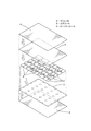
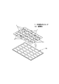
図面は、アンテナコイル及びICチップをカード基体中に埋設した非接触式ICカードのICチップ埋設方法を示し、図1、図2、図7に於いて、この非接触式ICカード1は、アンテナコイル2a及びICチップ2bを互いに接続してなる略矩形のインレット2と、インレット2の貼付け位置又は配列位置が片面にトンボ印刷されたPET−G樹脂製の下側コアシート3と、カード形状に打ち抜くための切取り位置(切取り線)がトンボ印刷されたPET−G樹脂製の上側コアシート3と、上下コアシート3,3の外側に積層される上下2枚のPET−G樹脂製のオーバーシート4,4とで構成される。なお、上述の貼付け位置及び切取り位置は、外側トンボや十字トンボ、コーナートンボ等のトンボ印刷で表示されるが、例えば四隅枠線、全体枠線、部分枠線、点線等で表示することもできる。
The drawings show an IC chip embedding method of a non-contact type IC card in which an antenna coil and an IC chip are embedded in a card base. In FIGS. 1, 2, and 7, the non-contact
上述のインレット2は、略47mm×略78mmのサイズにカット又は形成され、上下コアシート3,3は、略0.28mmの厚さに形成され、上下2枚のオーバーシート4,4は、略0.1mmの厚さに形成されている。且つ、PET−G樹脂シートを構成するコアシート3及びオーバーシート4は、インレット2の表裏両面の少なくとも一方の面が覆われる大きさ及び形状に形成している。なお、インレット2のサイズを、例えば略47mm以下又は以上に変更するか、略78mm以下又は以上のサイズに変更することもできる。また、コアシート3の厚みを、例えば略0.28mm以下又は以上の厚みに変更するか、オーバーシート4の厚みを、例えば略0.1mm以下又は以上の厚みに変更することもできる。
The
次に、上記非接触式ICカード1を構成するアンテナコイル2a及びICチップ2bの埋設方法を説明する。
Next, a method for embedding the
先ず、図1、図2にも示すように、アンテナコイル2a及びICチップ2bを互いに接続してなるインレット2…を、下側コアシート3の片面に印刷された貼付け位置にそれぞれ載置して複数枚配列又は多数枚配列した後、インレット2…及びコアシート3を積層状態に組み付けたまま、例えば接着剤で接着するか、ハンダコテで溶着する等して貼付け位置が変位しないように仮止めする。
First, as shown in FIGS. 1 and 2, the
次に、図3、図4にも示すように、下側オーバーシート4を、インレット2…が仮止めされた下側コアシート3の下面側に積層し、上側コアシート3を、下側コアシート3に仮止めされたインレット2…の上面側全体が覆われるように積層し、上側オーバーシート4を、上側コアシート3の上面側に積層した後、インレット2…及びコアシート3、オーバーシート4を積層状態に組み付けたまま仮止めして、積層体1Aを作る。なお、インレット2…の配列位置及びコアシート3,3、オーバーシート4,4の積層位置が変位しなければ、例えば2ケ所や3ヶ所、複数ヶ所、多数ヶ所等の所望する仮止めしてもよい。
Next, as shown in FIGS. 3 and 4, the
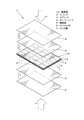
次に、図5に示すように、インレット2…及びコアシート3,3、オーバーシート4,4を積層してなる積層体1Aを、上下一対の鏡面板5,5間に挟み込み、その鏡面板5,5の外側に上下一対のクッション板6,6を積層した後、プレス手段を構成するプレス機7に投入して予備プレス及び本プレス、冷却プレスの順でプレス成形して製造する。なお、インレット2のICチップ2bが損傷及び破損しないような温度、圧力、時間で成形するのが好ましい。
Next, as shown in FIG. 5, the laminated
予備プレス時の温度を略135℃に設定し、圧力(面圧kg)を0kgに設定し、プレス時間を略90秒に設定して加熱及び加圧すると共に、インレット2の外周縁部よりも外側で対接する上下コアシート3,3の対向面を互いに溶融させ、上下に積層されたコアシート3及びオーバーシート4の対向面全体を互いに溶融させて一体的に接合する。つまり、同一の材質であるPET−G樹脂で形成したコアシート3,3の対向面と、コアシート3及びオーバーシート4の対向面とを互いに溶融させて溶着するので、強固に接合することができる。
The temperature at the time of preliminary pressing is set to about 135 ° C., the pressure (surface pressure kg) is set to 0 kg, the pressing time is set to about 90 seconds, and heating and pressurization are performed. The opposing surfaces of the upper and
次に、本プレス時の温度を略155℃に設定し、圧力(面圧kg)を略14kgに設定し、プレス時間を略90秒に設定して加熱及び加圧すると共に、インレット2のICチップ2bが覆われる部分に積層したコアシート3及びオーバーシート4を溶融して略均等に分散させ、略平坦且つ略平滑となる厚みに成形する。
Next, the temperature at the time of this press is set to about 155 ° C., the pressure (surface pressure kg) is set to about 14 kg, the press time is set to about 90 seconds, and heating and pressurization are performed. The
次に、冷却プレス時の温度を略20℃(PET−G樹脂が硬化する温度)に設定し、圧力(面圧kg)を略15kgに設定し、プレス時間を略90秒に設定して冷却及び加圧すると共に、インレット2のICチップ2bが覆われる部分に積層した少なくともオーバーシート4の外面を、本プレス時において略平坦となる厚みに加圧保持したまま積層体1A全体を硬化させ、積層体1Aの表裏両面を略平坦且つ略平滑となるように成形する。なお、予備プレス時及び本プレス時、冷却プレス時の温度(℃)及び圧力(kg)、時間(秒)を、実施例の温度及び圧力、時間以下又は以上に変更することもできる。
Next, the temperature at the time of the cooling press is set to about 20 ° C. (temperature at which the PET-G resin is cured), the pressure (surface pressure kg) is set to about 15 kg, and the press time is set to about 90 seconds for cooling. In addition, the
次に、プレス成形が完了した後、積層体1Aを、プレス機7から取り出して、上下一対の鏡面板5,5及び上下一対のクッション板6,6から外した後、図6、図7に示すように、積層体1Aを、上側コアシート3にトンボ印刷された切取り位置(切取り線)に沿ってカード形状に打ち抜き、インレット2及びコアシート3,3、オーバーシート4,4が一体的に積層されたカード基体1B…を積層体1Aから個々に分離して、所定サイズの非接触式ICカード1…を製造する。
Next, after the press molding is completed, the
なお、非接触式ICカード1の表裏両面に積層される少なくとも一方又は両方のオーバーシート4の表面には、例えばオフセット印刷やスクリーン印刷等の印刷方法で文字や図柄等をプレス成形前又はプレス成形後に印刷する。
In addition, on the surface of at least one or both
以上のように、アンテナコイル2a及びICチップ2bを互いに接続してなるインレット2…の表裏両面に、PET−G樹脂製のコアシート3,3及びオーバーシート4,4を積層し、インレット2のICチップ2bが覆われる部分に積層したコアシート3及びオーバーシート4をプレス機7で加圧及び加熱して略均等に分散させ、PET−G樹脂が硬化する温度でもって積層体1A全体を冷却し、ICチップ2bが覆われる部分に積層した少なくともオーバーシート4の外面を略平坦となる厚みに加圧保持したまま硬化させ、非接触式ICカード1及び積層体1Aの表裏両面が略平坦且つ略平滑となるように成形するので、従来例のようなICチップが覆われる部分に積層したシートの盛り上がり部分を切除するか、ICチップが露出されるような孔部をシートに形成するか、ICチップ上にメッシュシートを積層する等の工程及び部品が不要となり、工定数及び部品数が少なくなり、製造に要する時間を短縮して、製造コストの低減及び安価に製造することができる。
As described above, the
この発明の構成と、上述の実施例との対応において、
この発明のPET−G樹脂シートは、コアシート3及びオーバーシート4に対応し、
以下同様に、
プレス手段は、プレス機7に対応するも、
この発明は、上述の実施例の構成のみに限定されるものではない。
In the correspondence between the configuration of the present invention and the above-described embodiment,
The PET-G resin sheet of this invention corresponds to the
Similarly,
The press means corresponds to the
The present invention is not limited to the configuration of the above-described embodiment.
この発明の非接触式ICカードのICチップ埋設方法は、単一枚数の非接触式ICカードを製造する作業にも利用することができる。 The IC chip embedding method of the non-contact type IC card according to the present invention can also be used for an operation of manufacturing a single number of non-contact type IC cards.
1…非接触式ICカード
1A…積層体
1B…カード基体
2…インレット
2a…アンテナコイル
2b…ICチップ
3…コアシート
4…オーバーシート
5…鏡面板
6…クッション材
7…プレス機
DESCRIPTION OF
Claims (4)
上記アンテナコイル及びICチップを互いに接続してなるインレットの表裏両面にPET−G樹脂シートを積層し、
上記インレット及びPET−G樹脂シートを積層してなる積層体をプレス手段で略均等に加圧及び加熱し、
上記各PET−G樹脂シートの対向面を互いに溶融させて一体的に接合し、
上記ICチップが覆われる部分に積層したPET−G樹脂製シートを溶融して略均等に分散させた後、
上記PET−G樹脂が硬化する温度でもって積層体を略均等に冷却し、上記ICチップが覆われる部分に積層したPET−G樹脂シートの外面を略平坦となる厚みに加圧保持したまま硬化させ、該積層体の表裏両面を略平坦且つ略平滑に成形した
非接触式ICカードのICチップ埋設方法。 A non-contact IC card in which an antenna coil and an IC chip are embedded in a card base,
Laminating PET-G resin sheets on both the front and back surfaces of the inlet formed by connecting the antenna coil and the IC chip to each other;
The laminate formed by laminating the inlet and the PET-G resin sheet is pressed and heated approximately uniformly by a pressing means,
The opposing surfaces of each of the PET-G resin sheets are melted together and joined together,
After melting and dispersing the PET-G resin sheet laminated on the portion where the IC chip is covered approximately uniformly,
The laminate is cooled substantially uniformly at a temperature at which the PET-G resin is cured, and the outer surface of the PET-G resin sheet laminated on the portion where the IC chip is covered is cured while being pressed and held at a substantially flat thickness. An IC chip embedding method for a non-contact type IC card, wherein both surfaces of the laminate are formed to be substantially flat and substantially smooth.
上記アンテナコイル及びICチップを互いに接続してなるインレットの表裏両面に、PET−G樹脂製のコアシート及びオーバーシートを積層し、
上記インレット及びコアシート、オーバーシートを積層してなる積層体をプレス手段で略均等に加圧及び加熱し、
上記各コアシートの対向面と、上記コアシート及びオーバーシートの対向面とを互いに溶融させて一体的に接合し、
上記ICチップが覆われる部分に積層したコアシート及びオーバーシートを溶融して略均等に分散させた後、
上記PET−G樹脂が硬化する温度でもって積層体を略均等に冷却し、上記ICチップが覆われる部分に積層した少なくともオーバーシートの外面を略平坦となる厚みに加圧保持したまま硬化させ、該積層体の表裏両面を略平坦且つ略平滑に成形した
非接触式ICカードのICチップ埋設方法。 A non-contact IC card in which an antenna coil and an IC chip are embedded in a card base,
Laminating a PET-G resin core sheet and oversheet on both the front and back surfaces of the inlet formed by connecting the antenna coil and the IC chip to each other;
The laminate formed by laminating the inlet, the core sheet, and the oversheet is pressed and heated approximately uniformly by a pressing means,
The opposing surfaces of each of the core sheets and the opposing surfaces of the core sheet and the oversheet are melted together and integrally joined,
After melting the core sheet and the oversheet laminated on the portion where the IC chip is covered, and approximately evenly dispersing,
The laminate is cooled substantially uniformly at a temperature at which the PET-G resin is cured, and at least the outer surface of the oversheet laminated on the portion where the IC chip is covered is cured while being pressed and held at a substantially flat thickness, An IC chip embedding method for a non-contact type IC card in which both front and back surfaces of the laminate are formed substantially flat and substantially smooth.
請求項1記載の非接触式ICカードのICチップ埋設方法。 2. The IC chip embedding of a non-contact type IC card according to claim 1, wherein the PET-G resin sheet is composed of a PET-G resin core sheet and an oversheet having a size and shape that covers one side of the inlet. Method.
上記各コアシートの外面にオーバーシートを積層してなる積層体をプレス手段で加圧して略平坦且つ略平滑に成形した後、
上記プレス手段から取り出した積層体をカード形状に打ち抜いて非接触式ICカードに分離する
請求項1又は2記載の非接触式ICカードのICチップ埋設方法。
A plurality of the inlets are arranged at predetermined intervals between the opposing surfaces of the upper and lower core sheets,
After the laminate formed by laminating the oversheet on the outer surface of each of the core sheets is pressed with a pressing means to be formed substantially flat and substantially smooth,
3. The IC chip embedding method for a non-contact type IC card according to claim 1, wherein the laminate taken out from the pressing means is punched into a card shape and separated into a non-contact type IC card.
Priority Applications (1)
| Application Number | Priority Date | Filing Date | Title |
|---|---|---|---|
| JP2004109894A JP2005293396A (en) | 2004-04-02 | 2004-04-02 | Ic chip embedding method for non-contact ic card |
Applications Claiming Priority (1)
| Application Number | Priority Date | Filing Date | Title |
|---|---|---|---|
| JP2004109894A JP2005293396A (en) | 2004-04-02 | 2004-04-02 | Ic chip embedding method for non-contact ic card |
Publications (1)
| Publication Number | Publication Date |
|---|---|
| JP2005293396A true JP2005293396A (en) | 2005-10-20 |
Family
ID=35326230
Family Applications (1)
| Application Number | Title | Priority Date | Filing Date |
|---|---|---|---|
| JP2004109894A Pending JP2005293396A (en) | 2004-04-02 | 2004-04-02 | Ic chip embedding method for non-contact ic card |
Country Status (1)
| Country | Link |
|---|---|
| JP (1) | JP2005293396A (en) |
Cited By (3)
| Publication number | Priority date | Publication date | Assignee | Title |
|---|---|---|---|---|
| JP2009122974A (en) * | 2007-11-15 | 2009-06-04 | Toppan Printing Co Ltd | Manufacturing methods for inlays and information media (finished products) |
| JP2010176477A (en) * | 2009-01-30 | 2010-08-12 | Toppan Printing Co Ltd | Non-contact ic card and method of manufacturing the same |
| JP2011186590A (en) * | 2010-03-05 | 2011-09-22 | Dainippon Printing Co Ltd | Contactless ic card and method of manufacturing the same |
-
2004
- 2004-04-02 JP JP2004109894A patent/JP2005293396A/en active Pending
Cited By (3)
| Publication number | Priority date | Publication date | Assignee | Title |
|---|---|---|---|---|
| JP2009122974A (en) * | 2007-11-15 | 2009-06-04 | Toppan Printing Co Ltd | Manufacturing methods for inlays and information media (finished products) |
| JP2010176477A (en) * | 2009-01-30 | 2010-08-12 | Toppan Printing Co Ltd | Non-contact ic card and method of manufacturing the same |
| JP2011186590A (en) * | 2010-03-05 | 2011-09-22 | Dainippon Printing Co Ltd | Contactless ic card and method of manufacturing the same |
Similar Documents
| Publication | Publication Date | Title |
|---|---|---|
| KR100421706B1 (en) | Method for making cards and cards obtained by this method | |
| JP5395660B2 (en) | Method of manufacturing a card comprising at least one electronic module, assembly produced during the method, and intermediate product | |
| KR102649186B1 (en) | Recovered Plastic Cards | |
| US20100130288A1 (en) | Rfid-incorporated game token and manufacturing method thereof | |
| JP5130887B2 (en) | Non-contact IC inlet, non-contact IC inlet with cover, booklet with non-contact IC inlet, and manufacturing method thereof | |
| US6586078B2 (en) | High pressure lamination of electronic cards | |
| JP5884895B2 (en) | Card, card manufacturing method | |
| JP2005293396A (en) | Ic chip embedding method for non-contact ic card | |
| JP4156351B2 (en) | Non-contact IC card with rewrite recording layer and method of manufacturing non-contact IC card with rewrite recording layer | |
| JP4402367B2 (en) | Non-contact IC card | |
| RU2171497C2 (en) | Maps and method for producing maps | |
| JP2014160327A (en) | Laminate body, manufacturing method of laminate body | |
| JPH10337984A (en) | Circuit-containing type plastic card | |
| JP7809269B2 (en) | Security page and laminate thermocompression bonding method | |
| JP2000099680A (en) | Manufacture of non-contact type chip card | |
| JP2000231615A (en) | IC card | |
| JPS602347A (en) | Manufacture of card with recess | |
| JP2002074293A (en) | Manufacturing method of non-contact IC card | |
| JP3145100B2 (en) | IC card manufacturing method | |
| JP2004287573A (en) | IC card and manufacturing method thereof | |
| JP2009157562A (en) | Method of manufacturing tag sheet and tag sheet | |
| JP3910739B2 (en) | Contact IC card and manufacturing method thereof | |
| JP2003053600A (en) | Hot press plate, hot press device provided with the same, and sheet laminate | |
| JP5146224B2 (en) | Non-contact IC card manufacturing method | |
| JP2000182018A (en) | Method of manufacturing heat-resistant IC card |