JP2005292926A - Memory controller, flash memory system, and control method for flash memory - Google Patents
Memory controller, flash memory system, and control method for flash memory Download PDFInfo
- Publication number
- JP2005292926A JP2005292926A JP2004103308A JP2004103308A JP2005292926A JP 2005292926 A JP2005292926 A JP 2005292926A JP 2004103308 A JP2004103308 A JP 2004103308A JP 2004103308 A JP2004103308 A JP 2004103308A JP 2005292926 A JP2005292926 A JP 2005292926A
- Authority
- JP
- Japan
- Prior art keywords
- page
- flash memory
- writing
- write
- pages
- Prior art date
- Legal status (The legal status is an assumption and is not a legal conclusion. Google has not performed a legal analysis and makes no representation as to the accuracy of the status listed.)
- Granted
Links
- 230000015654 memory Effects 0.000 title claims abstract description 116
- 238000000034 method Methods 0.000 title claims description 116
- 230000006870 function Effects 0.000 claims description 8
- 238000010586 diagram Methods 0.000 description 9
- 238000006243 chemical reaction Methods 0.000 description 2
- 239000004065 semiconductor Substances 0.000 description 2
- XUIMIQQOPSSXEZ-UHFFFAOYSA-N Silicon Chemical compound [Si] XUIMIQQOPSSXEZ-UHFFFAOYSA-N 0.000 description 1
- 238000007599 discharging Methods 0.000 description 1
- 230000010365 information processing Effects 0.000 description 1
- 239000012212 insulator Substances 0.000 description 1
- 229910052710 silicon Inorganic materials 0.000 description 1
- 239000010703 silicon Substances 0.000 description 1
- 230000003068 static effect Effects 0.000 description 1
Images


Landscapes
- Techniques For Improving Reliability Of Storages (AREA)
Abstract
Description
本発明は、メモリコントローラ及びメモリコントローラを備えるフラッシュメモリシステム、並びに、フラッシュメモリの制御方法に関する。 The present invention relates to a memory controller, a flash memory system including the memory controller, and a flash memory control method.
近年、メモリーカードやシリコンディスクといったメモリシステムにて使用される半導体メモリに、フラッシュメモリが広く採用されている。フラッシュメモリは、不揮発性メモリの一種であり、フラッシュメモリに格納されたデータは、電力が供給されていないときでも保持されていることが要求される。 In recent years, flash memories have been widely adopted as semiconductor memories used in memory systems such as memory cards and silicon disks. A flash memory is a kind of non-volatile memory, and data stored in the flash memory is required to be held even when power is not supplied.
NAND型フラッシュメモリは、上記のメモリシステムで特に多く用いられるフラッシュメモリの一種である。NAND型フラッシュメモリに含まれている複数のメモリセルのそれぞれは、他のメモリセルとは独立して、論理値“1”を示すデータが格納されている消去状態から、論理値“0”を示すデータが格納されている書込状態へと変化することができる。 A NAND flash memory is a type of flash memory that is particularly frequently used in the above memory system. Each of the plurality of memory cells included in the NAND flash memory receives a logical value “0” from an erased state in which data indicating a logical value “1” is stored, independently of the other memory cells. It is possible to change to a writing state in which the indicated data is stored.
これとは対照的に、書込状態から消去状態へと変化するときには、各メモリセルは他のメモリセルと独立して変化することができない。このときには、ブロックと称される予め定められた数のメモリセルが、全て同時に消去状態になる。この一括消去動作は、一般的に、“ブロック消去”と称されている。
NAND型フラッシュメモリに対する書込処理若しくは読出処理は、ページと称される予め定められた数のメモリセル単位で処理が行なわれる。消去処理の単位であるブロックは複数のページで構成されている。
In contrast, when changing from the written state to the erased state, each memory cell cannot change independently of the other memory cells. At this time, all of a predetermined number of memory cells called blocks are simultaneously erased. This batch erase operation is generally called “block erase”.
The writing process or the reading process for the NAND flash memory is performed in units of a predetermined number of memory cells called pages. A block which is a unit of erasure processing is composed of a plurality of pages.
NAND型フラッシュメモリを用いたメモリシステムでは、突然の電源遮断等により、書込処理が中断される場合がある。このような場合、NAND型フラッシュメモリには、不完全な書込みデータが残されてしまう。その後、電源を投入したときに、このような不完全な書込みデータと正常な書込みデータを判別することが困難なときがある。 In a memory system using a NAND flash memory, the writing process may be interrupted due to a sudden power interruption or the like. In such a case, incomplete write data is left in the NAND flash memory. After that, when the power is turned on, it may be difficult to discriminate between such incomplete write data and normal write data.
このような問題を解消するために、下記特許文献1では、各ブロックの先頭ページ(冗長領域)に無効フラグを、最終ページ(冗長領域)に有効フラグを設け、正常に書込処理が終了したときに、有効フラグが有効となる設定処理を行ない、そのブロックのデータが不要となったときに、無効フラグが有効となる設定処理を行なっている。このようにすることにより、有効フラグが有効となる設定がなされているか否かにより、正常に書込処理が終了したか、又は中断したかを判別することができる。
特許文献1(特開2003−15929号公報)では、ブロック内の全ページにデータを書込んだときに有効フラグが有効となる設定処理を行なっているが、ブロック内の全ページにデータを書込まずに処理を終了させる場合もある。例えば、最初の処理で、ブロック内の一部のページにデータを書込んで処理を終了させ、次回の処理でその続きを書込む場合がある。このような場合、ブロック内の一部のページにデータを書込む処理が正常に終了したときには、有効フラグが有効となる設定処理は行なわれない。よって、その処理が正常に終了したかを判断することができない。 In Patent Document 1 (Japanese Patent Laid-Open No. 2003-15929), a setting process is performed in which the validity flag is valid when data is written to all pages in the block. However, data is written to all pages in the block. In some cases, the process may be terminated without being included. For example, in the first process, data may be written to some pages in the block to end the process, and the continuation may be written in the next process. In such a case, when the process of writing data to a part of the pages in the block ends normally, the setting process for enabling the valid flag is not performed. Therefore, it cannot be determined whether the process has been completed normally.
そこで、本発明は、ブロック内の一部のページにデータを書込む処理の場合でも、その処理が正常に行なわれたか否かを判断することができるメモリコントローラ及びメモリコントローラを備えるフラッシュメモリシステム、並びに、フラッシュメモリの制御方法を提供することを目的とする。 Therefore, the present invention provides a memory controller that can determine whether or not the process has been performed normally even in the case of a process of writing data to some pages in a block, and a flash memory system including the memory controller, It is another object of the present invention to provide a flash memory control method.
上記目的を達成するために、本発明の第1の観点に係るメモリコントローラは、ホストシステム側からの要求に基づいて、フラッシュメモリ内の同一ブロックに属する連続した複数ページに、データを書込む連続書込機能と、前記複数ページの書込開始ページの冗長領域に、書込終了ページを示す終点情報を設定する終点情報設定機能と、前記複数ページの書込終了ページの冗長領域に、該書込終了ページに対する書込処理が完了していることを示す処理完了情報を設定する処理完了情報設定機能と、を備えることを特徴とする。 In order to achieve the above object, the memory controller according to the first aspect of the present invention continuously writes data to a plurality of consecutive pages belonging to the same block in the flash memory based on a request from the host system side. A write function, an end point information setting function for setting end point information indicating a write end page in the redundant area of the write start page of the plurality of pages, and a write area in the redundant area of the write end page of the plurality of pages. And a process completion information setting function for setting process completion information indicating that the writing process for the inclusion end page has been completed.
なお、前記処理完了情報として、前記終点情報と同一の情報を用いてもよい。
また、前記複数ページの書込開始ページから書込終了ページまでの全ページの冗長領域に、前記終点情報を設定してもよい。
Note that the same information as the end point information may be used as the processing completion information.
The end point information may be set in a redundant area of all pages from the write start page to the write end page of the plurality of pages.
上記目的を達成するために、本発明の第2の観点に係るフラッシュメモリシステムは、本発明の第1の観点に係るメモリコントローラと、フラッシュメモリとを備えることを特徴とする。 In order to achieve the above object, a flash memory system according to a second aspect of the present invention comprises a memory controller according to the first aspect of the present invention and a flash memory.
上記目的を達成するために、本発明の第3の観点に係るフラッシュメモリの制御方法は、ホストシステム側からの要求に基づいて、フラッシュメモリ内の同一ブロックに属する連続した複数ページに、データを書込む連続書込処理と、前記複数ページの書込開始ページの冗長領域に、書込終了ページを示す終点情報を設定する終点情報設定処理と、前記複数ページの書込終了ページの冗長領域に、該書込終了ページに対する書込処理が完了していることを示す処理完了情報を設定する処理完了情報設定処理と、を含むことを特徴とする。 In order to achieve the above object, a flash memory control method according to a third aspect of the present invention provides data to a plurality of consecutive pages belonging to the same block in the flash memory based on a request from the host system side. A continuous writing process for writing, an end point information setting process for setting end point information indicating a write end page in the redundant area of the write start page of the plurality of pages, and a redundant area of the write end page of the plurality of pages. And a process completion information setting process for setting process completion information indicating that the writing process for the writing end page has been completed.
なお、前記処理完了情報として、前記終点情報と同一の情報を用いてもよい。
また、前記複数ページの書込開始ページから書込終了ページまでの全ページの冗長領域に、前記終点情報を設定してもよい。
Note that the same information as the end point information may be used as the processing completion information.
The end point information may be set in a redundant area of all pages from the write start page to the write end page of the plurality of pages.
本発明によれば、ホストシステム側からの要求に基づいて、フラッシュメモリ内の同一ブロックに属する連続した複数ページにデータを書込むときに、その書込処理の書込開始ページの冗長領域に、書込終了ページを示す終点情報を設定し、書込終了ページの冗長領域に、該書込終了ページに対する書込処理が完了していることを示す処理完了情報を設定している。このようにすることにより、書込開始ページの冗長領域に設定されている終点情報と、書込終了ページの冗長領域に設定されている処理完了情報の整合がとれているか否かで、その書込み処理が正常に行なわれたか否かを判断することができる。 According to the present invention, when data is written to a plurality of continuous pages belonging to the same block in the flash memory on the basis of a request from the host system side, in the redundant area of the write start page of the write process, End point information indicating the write end page is set, and process completion information indicating that the write process for the write end page is completed is set in the redundant area of the write end page. By doing so, the end point information set in the redundant area of the writing start page and the processing completion information set in the redundant area of the writing end page are determined depending on whether or not the writing is completed. It can be determined whether the process has been performed normally.
以下、図面に基づき、本発明の実施の形態について詳細に説明する。
[フラッシュメモリシステム1の説明]
図1は、本発明に係るフラッシュメモリシステム1を概略的に示すブロック図である。
Hereinafter, embodiments of the present invention will be described in detail with reference to the drawings.
[Description of flash memory system 1]
FIG. 1 is a block diagram schematically showing a
図1に示したように、フラッシュメモリシステム1は、フラッシュメモリ2とそれを制御するメモリコントローラ(以下、単にコントローラという)3とで構成されている。フラッシュメモリシステム1は、通常、ホストシステム4に着脱可能に装着されて使用され、ホストシステム4に対して一種の外部記憶装置として用いられる。
As shown in FIG. 1, the
尚、ホストシステム4としては、文字、音声、あるいは画像情報等の種々の情報を処理するパーソナルコンピュータやデジタルスチルカメラをはじめとする各種情報処理装置が挙げられる。 Examples of the host system 4 include various information processing apparatuses such as a personal computer and a digital still camera that process various information such as characters, sounds, and image information.
フラッシュメモリ2は、ページ単位で読出し又は書込みを、ブロック単位で消去を実行するデバイスであり、例えば、1ブロックは32ページで構成され、1ページは512バイトのユーザ領域と16バイトの冗長領域で構成されている。
The
コントローラ3は、ホストインターフェース制御ブロック5と、マイクロプロセッサ6と、ホストインターフェースブロック7と、ワークエリア8と、バッファ9と、フラッシュメモリインターフェースブロック10と、ECC(エラー・コレクション・コード)ブロック11と、フラッシュメモリシーケンサブロック12とから構成される。これら機能ブロックによって構成されるコントローラ3は、一つの半導体チップ上に集積されている。以下に各ブロックの機能を説明する。
The
マイクロプロセッサ6は、コントローラ3を構成する各機能ブロック全体の動作を制御する機能ブロックである。
ホストインターフェース制御ブロック5は、ホストインターフェースブロック7の動作を制御する機能ブロックである。ここで、ホストインターフェース制御ブロック5は、ホストインターフェースブロック7の動作を設定する動作設定レジスタ(図示せず)を備えており、この動作設定レジスタに基づきホストインターフェースブロック7は動作する。
The microprocessor 6 is a functional block that controls the operation of the entire functional blocks constituting the
The host interface control block 5 is a functional block that controls the operation of the
ホストインターフェースブロック7は、ホストシステム4とデータ、アドレス情報、ステータス情報及び外部コマンド情報の授受を行なう機能ブロックである。
すなわち、フラッシュメモリシステム1がホストシステム4に装着されると、フラッシュメモリシステム1とホストシステム4は、外部バス13を介して相互に接続され、かかる状態において、ホストシステム4よりフラッシュメモリシステム1に供給されるデータ等は、ホストインターフェースブロック7を入口としてコントローラ3の内部に取り込まれる。フラッシュメモリシステム1からホストシステム4に供給されるデータ等は、ホストインターフェースブロック7を出口としてホストシステム4に供給される。
The
That is, when the
さらに、ホストインターフェースブロック7は、ホストシステム4より供給されるホストアドレス及び外部コマンドを一時的に格納するタスクファイルレジスタ(図示せず)及びエラーが発生した場合にセットされるエラーレジスタ(図示せず)等を有している。
Further, the
ワークエリア8は、フラッシュメモリ2の制御に必要なデータが一時的に格納される作業領域であり、複数のSRAM(Static Random Access Memory)セルによって構成される機能ブロックである。
The
バッファ9は、フラッシュメモリ2から読出したデータ及びフラッシュメモリ2に書込むデータを一時的に保持する機能ブロックである。すなわち、フラッシュメモリ2から読出したデータは、ホストシステム4の受取準備ができるまでバッファ9に保持され、フラッシュメモリ2に書込むデータは、フラッシュメモリ2の書込準備ができるまでバッファ9に保持される。
The
フラッシュメモリシーケンサブロック12は、内部コマンドに基づきフラッシュメモリ2の動作を制御する機能ブロックである。フラッシュメモリシーケンサブロック12は、複数のレジスタ(図示せず)を備え、この複数のレジスタに内部コマンドを実行する際に必要な情報が設定される。この複数のレジスタに内部コマンドを実行する際に必要な情報が設定されると、フラッシュメモリシーケンサブロック12は、その情報に基づいて処理を実行する。ここで、「内部コマンド」とは、コントローラ3からフラッシュメモリ2に与えられるコマンドであり、ホストシステム4からフラッシュメモリシステム1に与えられるコマンドである「外部コマンド」と区別される。
The flash
フラッシュメモリインターフェースブロック10は、内部バス14を介して、フラッシュメモリ2とデータ、アドレス情報、ステータス情報、内部コマンド情報及びデバイスID情報等の授受を行う機能ブロックである。
The flash memory interface block 10 is a functional block that exchanges data, address information, status information, internal command information, device ID information, and the like with the
ECCブロック11は、フラッシュメモリ2に書込むデ―タに付加されるエラーコレクションコードを生成するとともに、読出しデータに付加されたエラーコレクションコードに基づいて、読出したデータに含まれる誤りを検出・訂正する機能ブロックである。
The
[フラッシュメモリ2の説明]
フラッシュメモリ2は、NAND型フラッシュメモリであり、ストレージデバイスへの用途として(ハードディスクの代わりになるものとして)開発された不揮発性メモリである。NAND型フラッシュメモリは、ランダムアクセスを行なうことができず、書込みと読出しはページ単位で、消去はブロック単位で行なわれる。又、データの上書きができないので、データを書込むときは、消去されている領域にデータの書込みが行なわれる。
[Description of flash memory 2]
The
フラッシュメモリ2は、このような特徴を有するため、通常、データの書替を行なう場合には、ブロック消去されている消去済ブロックに新たなデータ(書替後のデータ)を書込み、古いデータ(書替前のデータ)が書込まれていたブロックを消去するという処理を行なっている。
Since the
このようなデータの書替を行なった場合、書替後のデータは書替前と異なるブロックに書込まれるため、ホストシステム4側から与えられるアドレスに基づく論理ブロックアドレスと、フラッシュメモリ2内でのブロックアドレスである物理ブロックアドレスとの対応関係は、データを書替える毎に動的に変化する。この論理ブロックアドレスと物理ブロックアドレスとの対応関係は、通常、その対応関係を示したアドレス変換テーブルによって管理されており、アドレス変換テーブルは、後述する対応論理ブロックアドレスに基づいて作成される。
When such data rewriting is performed, the data after rewriting is written in a block different from that before rewriting. Therefore, the logical block address based on the address given from the host system 4 side and the
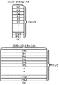
ここで、上記ブロックとページの関係を図2を参照して説明する。
図2(a),(b)は、ブロック及びページの関係を説明する説明図である。
フラッシュメモリにおけるブロックとページの関係は、フラッシュメモリの仕様によって異なるが、一般的なフラッシュメモリでは、図2(a)に示したように、1ブロックが32ページ(P0〜P31)で構成され、各ページが512バイトのユーザ領域と16バイトの冗長領域で構成されている。
Here, the relationship between the block and the page will be described with reference to FIG.
2A and 2B are explanatory diagrams for explaining the relationship between blocks and pages.
The relationship between the block and the page in the flash memory differs depending on the specification of the flash memory, but in a general flash memory, as shown in FIG. 2A, one block is composed of 32 pages (P0 to P31), Each page includes a 512-byte user area and a 16-byte redundant area.
又、記憶容量の増加に伴い、図2(b)に示したように、1ブロックが64ページ(P0〜P63)で構成され、各ページが2048バイトのユーザ領域と64バイトの冗長領域で構成されているものも提供されている。
ユーザ領域は、主に、ホストシステム4から供給されるデ―タが記憶される領域であり、冗長領域は、エラーコレクションコード、対応論理ブロックアドレス及びブロックステータス等の付加データが記憶される領域である。エラ―コレクションコードは、ユーザ領域に記憶されているデータに含まれる誤りを検出、訂正するための付加データであり、外部のECCブロックによって生成される。対応論理ブロックアドレスは、そのブロックにデータが格納されている場合に、そのブロックがどの論理ブロックアドレスに対応するかを示している。
As the storage capacity increases, as shown in FIG. 2B, one block is composed of 64 pages (P0 to P63), and each page is composed of a 2048-byte user area and a 64-byte redundant area. What is being provided is also provided.
The user area is mainly an area for storing data supplied from the host system 4, and the redundant area is an area for storing additional data such as an error correction code, a corresponding logical block address and a block status. is there. The error collection code is additional data for detecting and correcting an error included in the data stored in the user area, and is generated by an external ECC block. The corresponding logical block address indicates to which logical block address the block corresponds when data is stored in the block.
尚、そのブロックにデータが格納されていない場合は、対応論理ブロックアドレスも格納されていないので、対応論理ブロックアドレスが格納されているか否かで、そのブロックが消去済ブロックであるか否かを判断することもできる。つまり、対応論理ブロックアドレスが格納されていない場合は、消去済ブロックであると判断される。ブロックステータスは、そのブロックが不良ブロック(正常にデータの書込み等を行なうことができないブロック)であるか否かを示すフラグであり、そのブロックが不良ブロックであると判断された場合には、不良ブロックであることを示すフラグが設定される。 If no data is stored in the block, the corresponding logical block address is not stored. Therefore, whether or not the block is an erased block depends on whether or not the corresponding logical block address is stored. It can also be judged. That is, if the corresponding logical block address is not stored, it is determined that the block is an erased block. The block status is a flag indicating whether or not the block is a bad block (a block in which data cannot be normally written). If it is determined that the block is a bad block, the block status is bad. A flag indicating a block is set.
次に、フラッシュメモリ2の回路構成について説明する。フラッシュメモリ2は、一般的なNAND型フラッシュメモリと同様に、書込みデータ若しくは読出しデータを保持するためのレジスタと、データを記憶するメモリセルアレイとによって構成されている。
Next, the circuit configuration of the
メモリセルアレイは、複数のメモリセルが直列に接続されたメモリセル群を複数備えており、ワード線によってメモリセル群の特定のメモリセルが選択される。このワード線によって選択されたメモリセルとレジスタの間で、データの複写(レジスタからメモリセルへの複写、若しくはメモリセルからレジスタへの複写)が行なわれる。 The memory cell array includes a plurality of memory cell groups in which a plurality of memory cells are connected in series, and a specific memory cell in the memory cell group is selected by a word line. Data copying (copying from the register to the memory cell or copying from the memory cell to the register) is performed between the memory cell selected by the word line and the register.
メモリセルアレイを構成するメモリセルは、2つのゲートを備えたMOSトランジスタで構成されている。ここで、上側のゲートはコントロールゲートと、下側のゲートはフローティングゲートと呼ばれており、フローティングゲートに電荷(電子)を注入若しくはフローティングゲートから電荷(電子)を排出することによって、データの書込み若しくはデータの消去を行なっている。 A memory cell constituting the memory cell array is composed of a MOS transistor having two gates. Here, the upper gate is called a control gate and the lower gate is called a floating gate. Data is written by injecting charges (electrons) into the floating gate or discharging charges (electrons) from the floating gate. Or data is erased.
フローティングゲートは周囲を絶縁体で囲まれているので、注入された電子は長期間にわたって保持される。尚、フローティングゲートに電子を注入するときは、コントロールゲートが高電位側となる高電圧を印加して電子を注入し、フローティングゲートから電子を排出するときは、コントロールゲートが低電位側となる高電圧を印加して電子を排出する。ここで、フローティングゲートに電子が注入されている状態(書込状態)が、論理値の「0」のデータに対応し、フローティングゲートから電子が排出されている状態(消去状態)が、論理値の「1」のデータに対応する。 Since the floating gate is surrounded by an insulator, the injected electrons are held for a long period of time. When electrons are injected into the floating gate, a high voltage is applied so that the control gate is on the high potential side. When electrons are injected from the floating gate, electrons are injected on the floating gate. A voltage is applied to discharge electrons. Here, the state in which electrons are injected into the floating gate (write state) corresponds to the data of the logical value “0”, and the state in which electrons are discharged from the floating gate (erased state) is the logical value. Corresponds to the data of “1”.
[動作説明]
フラッシュメモリシステム1では、ホストシステム4側からの要求に基づいて、フラッシュメモリ2内の同一ブロックに属する連続した複数ページにデータを書込む書込処理を行なうときに、その書込処理の書込開始ページの冗長領域に、書込終了ページを示す終点情報を設定し、書込終了ページの冗長領域に、該書込終了ページに対する書込処理が完了していることを示す処理完了情報を設定する。以下に、この終点情報と処理完了情報について図面を参照して説明する。
[Description of operation]
In the
図3は、フラッシュメモリ2内のページの冗長領域に設定される終点情報と処理完了情報の一例を示す図である。
図3では、32個のページで構成されたブロックに対して、ステップ1〜3の書込処理を行なっている。例えば、ステップ1では、ページ0〜10(P0〜P10の11個のページ)のユーザ領域にデータが書込まれ、ステップ2では、ページ11〜23(P11〜P23の13個のページ)のユーザ領域にデータが書込まれ、ステップ3では、ページ24〜31(P24〜P31の8個のページ)のユーザ領域にデータが書込まれる。
FIG. 3 is a diagram showing an example of end point information and processing completion information set in a redundant area of a page in the
In FIG. 3, the writing process in
各ページのユーザ領域にデータを書込むときに、終点情報若しくは処理完了情報に対応する情報が冗長領域に設定される。ステップ1の書込処理では、書込開始ページであるページ0(P0)から書込終了ページであるページ10(P10)までの全ての冗長領域に、次回の書込処理(ステップ2)で書込みが開始されるページのページの番号である11(2進数の01011b)が設定される。この11(2進数の01011b)は、書込み開始ページに、書込み対象のページ数を加算した値であり、書込終了ページに対応する。
When data is written in the user area of each page, information corresponding to end point information or processing completion information is set in the redundant area. In the writing process in
ステップ1と同様、ステップ2の書込処理では、書込開始ページであるページ11(P11)から書込終了ページであるページ23(P23)までの全ての冗長領域に、次回の書込処理(ステップ3)で書込みが開始されるページの番号である24(2進数の11000b)が設定される。
ステップ3の書込処理では、このブロックの最終ページであるページ31(P31)までデータが書込まれるので、書込開始ページであるページ24(P24)から書込終了ページであるページ31(P31)までの全ての冗長領域に、0(2進数の00000b)が設定される。ここで、書込処理の書込終了ページが、そのブロックの最終ページである場合、次回の書込処理で書込みが開始されるページの番号として0(2進数の00000b)を設定している。
As in
In the write process in
この例では、終点情報に対応する情報として、次回の書込処理で書込みが開始されるページの番号を用い、処理完了情報に対応する情報についても、次回の書込処理で書込みが開始されるページの番号を用いている。
このようにした場合、書込開始ページの冗長領域に設定されているページ番号の1個前のページが書込終了ページに対応するので、書込開始ページの冗長領域に設定されているページ番号の、1個前のページの冗長領域に、書込開始ページと同一のページ番号が設定されていれば、書込開始ページから書込終了ページまでの書込処理が正常に行われたと判断できる。
In this example, the page number where writing is started in the next writing process is used as the information corresponding to the end point information, and the writing corresponding to the processing completion information is also started in the next writing process. The page number is used.
In this case, the page number immediately before the page number set in the redundant area of the write start page corresponds to the write end page, so the page number set in the redundant area of the write start page If the same page number as the writing start page is set in the redundant area of the previous page, it can be determined that the writing process from the writing start page to the writing end page has been performed normally. .
つまり、ステップ1で、ステップ1の書込開始ページであるページ0(P0)の冗長領域に、11(2進数の01011b)が設定されていた場合、ページ10(P10)がステップ1の書込終了ページに対応するので、ページ10(P10)の冗長領域に11(2進数の01011b)が設定されていれば、ステップ1の書込処理が正常に行われたと判断できる。ステップ2で、ステップ2の書込開始ページであるページ11(P11)の冗長領域に、24(2進数の11000b)が設定されていた場合、ページ23(P23)がステップ2の書込終了ページに対応するので、ページ23(P23)の冗長領域に24(2進数の11000b)が設定されていれば、ステップ2の書込処理が正常に行われたと判断できる。
That is, if 11 (binary 01011b) is set in the redundant area of page 0 (P0), which is the write start page of
ステップ3で、ステップ3の書込開始ページであるページ24(P24)の冗長領域に、0(2進数の00000b)が設定されていた場合、ページ31(P31)がステップ3の書込終了ページに対応するので、ページ31(P31)の冗長領域に0(2進数の00000b)が設定されていれば、ステップ3の書込処理が正常に行われたと判断てきる。
If 0 (binary 00000b) is set in the redundant area of page 24 (P24) which is the write start page of
次に、書込処理が途中で中断した場合について、図4を参照して説明する。
図4は、書込処理中に処理が中断した場合の冗長領域の設定状態(その1)を示す図である。
ステップ2の書込処理では、ページ11〜23(P11〜P23)のユーザ領域にデータが書込まれるので、ページ11〜23の冗長領域に、次回の書込処理で書込みが開始されるページの番号である24(2進数の11000b)が設定される。ここで、ユーザ領域に対する書込処理と冗長領域に対する書込処理は同時進行するので、ユーザ領域に対する書込処理が途中で中断したときには、同様に冗長領域に対する書込処理も中断する。
Next, a case where the writing process is interrupted will be described with reference to FIG.
FIG. 4 is a diagram showing a redundant area setting state (part 1) when the process is interrupted during the writing process.
In the writing process of
図4に示した例では、ページ11〜19(P11〜P19)の冗長領域に、次回の書込処理で書込みが開始されるページの番号である24(2進数の11000b)が設定されているが、ページ20〜23(P20〜P23)の冗長領域には、24(2進数の11000b)が設定されていない。従って、ステップ2の書込処理は、ページ19(P19)に対する書込処理が終了した後に処理が中断したと判断することができる。つまり、書込終了ページ以外のページの冗長領域にも処理完了情報を設定すれば、書込処理が中断したときの処理の進行状況を検知することができる。
In the example shown in FIG. 4, 24 (binary number 11000b), which is the page number where writing is started in the next writing process, is set in the redundant areas of
図3の例では、書込開始ページから書込終了ページまでの全て冗長領域に同じ値を設定していたが、書込開始ページと書込終了ページとの間に存在するページの冗長領域には、終点情報若しくは処理完了情報を設定しない構成にしてもよい(図5参照)。 In the example of FIG. 3, the same value is set for all the redundant areas from the writing start page to the writing end page, but the redundant area of the page existing between the writing start page and the writing end page is set. May be configured not to set end point information or processing completion information (see FIG. 5).
図5は、書込処理中に処理が中断した場合の冗長領域の設定状態(その2)を示す図である。
図5の例では、書込終了ページ以外のページの冗長領域には処理完了情報を設定していない(2進数の11111b)。このようにした場合、書込処理が中断したときの処理の進行状況を検知することはできないが、書込処理が正常に終了したか否かは判断することができる。
FIG. 5 is a diagram showing a redundant area setting state (part 2) when the process is interrupted during the writing process.
In the example of FIG. 5, the processing completion information is not set in the redundant areas of pages other than the write end page (binary number 11111b). In this case, the progress of the process when the writing process is interrupted cannot be detected, but it can be determined whether or not the writing process has ended normally.
つまり、ステップ2の書込処理の書込開始ページであるページ11(P11)の冗長領域には、次回の書込処理で書込みが開始されるページの番号である24(2進数の11000b)が設定されているが、書込終了ページであるページ23(P23)の冗長領域には、処理完了情報として24(2進数の11000b)が設定されていないので、ステップ2の書込処理は途中で中断したと判断することができる。
That is, in the redundant area of page 11 (P11) which is the write start page of the write process in
図3〜図5では、書込開始ページの冗長領域に設定される終点情報と書込終了ページの冗長領域に設定する処理完了情報とを同じにした場合を説明したが、終点情報と書込完了情報とを異ならせてもよい。その例を、図6〜図8を用いて説明する。 3 to 5, the end point information set in the redundant area of the write start page and the processing completion information set in the redundant area of the write end page have been described as being the same. The completion information may be different. Examples thereof will be described with reference to FIGS.
図6は、フラッシュメモリ内のページの冗長領域に設定される終点情報と処理完了情報の他の例を示す図である。
図6に示した例では、終点情報に対応する情報として、次回の書込処理で書込みが開始されるページの番号を用い、処理完了情報に対応する情報として、冗長領域に0(2進数の00000b)を設定し、書込開始ページを除いた書込終了ページまでの全てのページの冗長領域に書込んでいる。この場合、書込開始ページの冗長領域に設定されているページ番号の、1個前のページの冗長領域に、(2進数の00000b)が設定されていれば、書込開始ページから書込終了ページまでの書込処理が正常に行われたと判断できる。
FIG. 6 is a diagram showing another example of the end point information and the processing completion information set in the page redundancy area in the flash memory.
In the example shown in FIG. 6, the page number where writing is started in the next writing process is used as information corresponding to the end point information, and 0 (binary number) is stored in the redundant area as information corresponding to the processing completion information. 00000b) is set, and data is written in the redundant areas of all pages up to the write end page except the write start page. In this case, if (binary number 00000b) is set in the redundant area of the previous page of the page number set in the redundant area of the writing start page, writing ends from the writing start page. It can be determined that the writing process up to the page has been performed normally.
つまり、ステップ1で、ステップ1の書込開始ページであるページ0(P0)の冗長領域に、11(2進数の01011b)が設定されていた場合、ページ10(P10)の冗長領域に0(2進数の00000b)が設定されていれば、ステップ1の書込処理が正常に行われたと判断できる。
That is, if 11 (binary 01011b) is set in the redundant area of page 0 (P0) which is the write start page of
ステップ2で、ステップ2の書込開始ページであるページ11(P11)の冗長領域に、24(2進数の11000b)が設定されていた場合、ページ23(P23)の冗長領域に0(2進数の00000b)が設定されていれば、ステップ2の書込処理が正常に行われたと判断できる。
In
ステップ3で、ステップ3の書込開始ページであるページ24(P24)の冗長領域に、0(2進数の00000b)が設定されていた場合、ページ31(P31)の冗長領域に0(2進数の00000b)が設定されていれば、ステップ3の書込処理が正常に行われたと判断できる。
In
図7は、書込処理中に処理が中断した場合の冗長領域の設定状態(その3)を示す図である。
図7のステップ2の書込処理でページ11〜23(P11〜P23)のユーザ領域にデータを書込む予定であったが、ページ20の書込みが完了した段階で処理が中断された場合、ページ12〜20(P12〜P20)の冗長領域には、0(2進数の00000b)が設定されているが、ページ21〜23(P21〜P23)の冗長領域には、0(2進数の00000b)が設定されていない。従って、ステップ2の書込処理は、ページ20(P20)に対する書込処理が終了した後に処理が中断したと判断することができる。つまり、書込終了ページ以外のページの冗長領域にも処理完了情報を設定すれば、書込処理が中断したときの処理の進行状況を検知することができる。
FIG. 7 is a diagram showing a redundant area setting state (part 3) when the process is interrupted during the writing process.
If the write processing in
図6の例では、書込開始ページを除く書込終了ページまでの全ての冗長領域に同じ値を設定していたが、書込開始ページと書込終了ページとの間に存在するページの冗長領域には、終点情報若しくは処理完了情報を設定しない構成にしてもよい(図8参照)。 In the example of FIG. 6, the same value is set for all the redundant areas up to the write end page except the write start page. However, the redundancy of the page existing between the write start page and the write end page is set. The area may be configured not to set end point information or processing completion information (see FIG. 8).
図8は、書込処理中に処理が中断した場合の冗長領域の設定状態(その4)を示す図である。
図8のように、書込終了ページ以外のページの冗長領域には処理完了情報を設定していない。このようにした場合、書込処理が中断したときの処理の進行状況を検知することはできないが、書込処理が正常に終了したか否かは判断することができる。
FIG. 8 is a diagram showing a redundant area setting state (part 4) when the process is interrupted during the writing process.
As shown in FIG. 8, processing completion information is not set in the redundant areas of pages other than the write end page. In this case, the progress of the process when the writing process is interrupted cannot be detected, but it can be determined whether or not the writing process has ended normally.
つまり、ステップ2の書込処理の書込開始ページであるページ11(P11)の冗長領域には、次回の書込処理で書込みが開始されるページの番号である24(2進数の11000b)が設定されているが、書込終了ページであるページ23(P23)の冗長領域には、処理完了情報として0(2進数の00000b)が設定されていないので、ステップ2の書込処理は途中で中断したと判断することができる。
That is, in the redundant area of page 11 (P11) which is the write start page of the write process in
尚、以上の説明では、終点情報として次回の書込処理で書込みが開始されるページの番号を用いたが、終点情報は直接的若しくは間接的に書込終了ページを示している情報であれば、他の情報であってもよい。例えば、終点情報として書込終了ページの番号等を用いてもよい。処理完了情報についても、上述の例に限定されず、書込終了ページの番号等を用いてもよい。 In the above description, the page number at which writing is started in the next writing process is used as the end point information. However, the end point information is information indicating the write end page directly or indirectly. Other information may be used. For example, the write end page number or the like may be used as the end point information. The processing completion information is not limited to the above example, and the number of the write end page may be used.
1 フラッシュメモリシステム
2 フラッシュメモリ
3 メモリコントローラ
4 ホストシステム
1
Claims (7)
前記複数ページの書込開始ページの冗長領域に、書込終了ページを示す終点情報を設定する終点情報設定機能と、
前記複数ページの書込終了ページの冗長領域に、該書込終了ページに対する書込処理が完了していることを示す処理完了情報を設定する処理完了情報設定機能と、
を備えることを特徴とするメモリコントローラ。 Based on a request from the host system side, a continuous writing function for writing data to a plurality of continuous pages belonging to the same block in the flash memory,
An end point information setting function for setting end point information indicating a write end page in a redundant area of the write start page of the plurality of pages;
A process completion information setting function for setting process completion information indicating that the writing process for the write end page is completed in the redundant area of the write end page of the plurality of pages;
A memory controller comprising:
前記複数ページの書込開始ページの冗長領域に、書込終了ページを示す終点情報を設定する終点情報設定処理と、
前記複数ページの書込終了ページの冗長領域に、該書込終了ページに対する書込処理が完了していることを示す処理完了情報を設定する処理完了情報設定処理と、
を含むことを特徴とするフラッシュメモリの制御方法。 Based on a request from the host system side, a continuous writing process for writing data to a plurality of continuous pages belonging to the same block in the flash memory;
End point information setting processing for setting end point information indicating a write end page in the redundant area of the write start page of the plurality of pages;
A process completion information setting process for setting process completion information indicating that the write process for the write end page is completed in the redundant area of the write end page of the plurality of pages;
A method for controlling a flash memory, comprising:
7. The flash memory control method according to claim 5, wherein the end point information is set in a redundant area of all pages from the write start page to the write end page of the plurality of pages.
Priority Applications (1)
| Application Number | Priority Date | Filing Date | Title |
|---|---|---|---|
| JP2004103308A JP4194518B2 (en) | 2004-03-31 | 2004-03-31 | Memory controller, flash memory system, and flash memory control method |
Applications Claiming Priority (1)
| Application Number | Priority Date | Filing Date | Title |
|---|---|---|---|
| JP2004103308A JP4194518B2 (en) | 2004-03-31 | 2004-03-31 | Memory controller, flash memory system, and flash memory control method |
Publications (2)
| Publication Number | Publication Date |
|---|---|
| JP2005292926A true JP2005292926A (en) | 2005-10-20 |
| JP4194518B2 JP4194518B2 (en) | 2008-12-10 |
Family
ID=35325828
Family Applications (1)
| Application Number | Title | Priority Date | Filing Date |
|---|---|---|---|
| JP2004103308A Expired - Fee Related JP4194518B2 (en) | 2004-03-31 | 2004-03-31 | Memory controller, flash memory system, and flash memory control method |
Country Status (1)
| Country | Link |
|---|---|
| JP (1) | JP4194518B2 (en) |
Cited By (3)
| Publication number | Priority date | Publication date | Assignee | Title |
|---|---|---|---|---|
| JP2007257283A (en) * | 2006-03-23 | 2007-10-04 | Tdk Corp | Memory controller and flash memory system |
| JP2008276371A (en) * | 2007-04-26 | 2008-11-13 | Tdk Corp | MEMORY CONTROLLER, FLASH MEMORY SYSTEM HAVING MEMORY CONTROLLER, AND FLASH MEMORY CONTROL METHOD |
| WO2014024350A1 (en) * | 2012-08-07 | 2014-02-13 | パナソニック株式会社 | Recording device, access device, recording system, and recording method |
-
2004
- 2004-03-31 JP JP2004103308A patent/JP4194518B2/en not_active Expired - Fee Related
Cited By (5)
| Publication number | Priority date | Publication date | Assignee | Title |
|---|---|---|---|---|
| JP2007257283A (en) * | 2006-03-23 | 2007-10-04 | Tdk Corp | Memory controller and flash memory system |
| JP2008276371A (en) * | 2007-04-26 | 2008-11-13 | Tdk Corp | MEMORY CONTROLLER, FLASH MEMORY SYSTEM HAVING MEMORY CONTROLLER, AND FLASH MEMORY CONTROL METHOD |
| WO2014024350A1 (en) * | 2012-08-07 | 2014-02-13 | パナソニック株式会社 | Recording device, access device, recording system, and recording method |
| JPWO2014024350A1 (en) * | 2012-08-07 | 2016-07-25 | パナソニックIpマネジメント株式会社 | Recording apparatus, access apparatus, recording system, and recording method |
| US9778857B2 (en) | 2012-08-07 | 2017-10-03 | Panasonic intellectual property Management co., Ltd | Recording device, access device, recording system, and recording method |
Also Published As
| Publication number | Publication date |
|---|---|
| JP4194518B2 (en) | 2008-12-10 |
Similar Documents
| Publication | Publication Date | Title |
|---|---|---|
| US8125825B2 (en) | Memory system protected from errors due to read disturbance and reading method thereof | |
| JP2006018373A (en) | Memory controller, flash memory system and control method for flash memory | |
| JP4373943B2 (en) | Memory controller, flash memory system, and flash memory control method | |
| JP4697146B2 (en) | MEMORY CONTROLLER, FLASH MEMORY SYSTEM HAVING MEMORY CONTROLLER, AND FLASH MEMORY CONTROL METHOD | |
| JP4177360B2 (en) | Memory controller, flash memory system, and flash memory control method | |
| JP4194518B2 (en) | Memory controller, flash memory system, and flash memory control method | |
| JP2006155335A (en) | Memory controller, flash memory system, and control method thereof | |
| JP4661369B2 (en) | Memory controller | |
| JP2010128697A (en) | Memory system | |
| JP4177292B2 (en) | MEMORY CONTROLLER, FLASH MEMORY SYSTEM, AND FLASH MEMORY CONTROL METHOD | |
| JP4544167B2 (en) | Memory controller and flash memory system | |
| JP2005292925A (en) | Memory controller, flash memory system, and control method for flash memory | |
| JP4661497B2 (en) | Memory controller, flash memory system, and flash memory control method | |
| JP2006221334A (en) | Memory controller, flash memory system, and control method for flash memory | |
| JP4177301B2 (en) | Memory controller, flash memory system, and flash memory control method | |
| JP4000124B2 (en) | MEMORY CONTROLLER, FLASH MEMORY SYSTEM PROVIDED WITH MEMORY CONTROLLER, AND FLASH MEMORY CONTROL METHOD | |
| JP4332108B2 (en) | Memory controller, flash memory system, and flash memory control method | |
| JP4609406B2 (en) | MEMORY CONTROLLER, FLASH MEMORY SYSTEM PROVIDED WITH MEMORY CONTROLLER, AND FLASH MEMORY CONTROL METHOD | |
| JP2006178909A (en) | Memory controller, flash memory system and method for controlling flash memory | |
| JP4304167B2 (en) | Memory controller, flash memory system, and flash memory control method | |
| JP4366283B2 (en) | Memory controller and flash memory system including the memory controller | |
| JP2005293177A (en) | Memory controller and flash memory system | |
| JP4273038B2 (en) | Memory controller, flash memory system, and flash memory data transfer method | |
| JP4254930B2 (en) | Memory controller, flash memory system, and flash memory control method | |
| JP4245594B2 (en) | Memory controller and flash memory system |
Legal Events
| Date | Code | Title | Description |
|---|---|---|---|
| A621 | Written request for application examination |
Free format text: JAPANESE INTERMEDIATE CODE: A621 Effective date: 20060313 |
|
| A977 | Report on retrieval |
Free format text: JAPANESE INTERMEDIATE CODE: A971007 Effective date: 20080910 |
|
| TRDD | Decision of grant or rejection written | ||
| A01 | Written decision to grant a patent or to grant a registration (utility model) |
Free format text: JAPANESE INTERMEDIATE CODE: A01 Effective date: 20080916 |
|
| A01 | Written decision to grant a patent or to grant a registration (utility model) |
Free format text: JAPANESE INTERMEDIATE CODE: A01 |
|
| A61 | First payment of annual fees (during grant procedure) |
Free format text: JAPANESE INTERMEDIATE CODE: A61 Effective date: 20080922 |
|
| R150 | Certificate of patent or registration of utility model |
Ref document number: 4194518 Country of ref document: JP Free format text: JAPANESE INTERMEDIATE CODE: R150 Free format text: JAPANESE INTERMEDIATE CODE: R150 |
|
| FPAY | Renewal fee payment (event date is renewal date of database) |
Free format text: PAYMENT UNTIL: 20111003 Year of fee payment: 3 |
|
| FPAY | Renewal fee payment (event date is renewal date of database) |
Free format text: PAYMENT UNTIL: 20121003 Year of fee payment: 4 |
|
| FPAY | Renewal fee payment (event date is renewal date of database) |
Free format text: PAYMENT UNTIL: 20121003 Year of fee payment: 4 |
|
| FPAY | Renewal fee payment (event date is renewal date of database) |
Free format text: PAYMENT UNTIL: 20131003 Year of fee payment: 5 |
|
| LAPS | Cancellation because of no payment of annual fees |