JP2005292004A - 試験装置及び設定方法 - Google Patents
試験装置及び設定方法 Download PDFInfo
- Publication number
- JP2005292004A JP2005292004A JP2004109297A JP2004109297A JP2005292004A JP 2005292004 A JP2005292004 A JP 2005292004A JP 2004109297 A JP2004109297 A JP 2004109297A JP 2004109297 A JP2004109297 A JP 2004109297A JP 2005292004 A JP2005292004 A JP 2005292004A
- Authority
- JP
- Japan
- Prior art keywords
- device under
- under test
- signal
- equalizer
- reference voltage
- Prior art date
- Legal status (The legal status is an assumption and is not a legal conclusion. Google has not performed a legal analysis and makes no representation as to the accuracy of the status listed.)
- Granted
Links
- 238000012360 testing method Methods 0.000 title claims abstract description 203
- 238000000034 method Methods 0.000 title claims description 16
- 230000005540 biological transmission Effects 0.000 claims description 44
- 230000003321 amplification Effects 0.000 claims description 34
- 238000003199 nucleic acid amplification method Methods 0.000 claims description 34
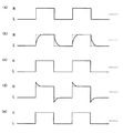
- 230000003111 delayed effect Effects 0.000 abstract description 5
- 238000010586 diagram Methods 0.000 description 8
- 230000004048 modification Effects 0.000 description 6
- 238000012986 modification Methods 0.000 description 6
- 230000002238 attenuated effect Effects 0.000 description 3
- 230000008054 signal transmission Effects 0.000 description 2
- 238000006243 chemical reaction Methods 0.000 description 1
- 230000001934 delay Effects 0.000 description 1
- 230000001419 dependent effect Effects 0.000 description 1
- 230000002542 deteriorative effect Effects 0.000 description 1
- 238000004519 manufacturing process Methods 0.000 description 1
Images


Classifications
-
- G—PHYSICS
- G01—MEASURING; TESTING
- G01R—MEASURING ELECTRIC VARIABLES; MEASURING MAGNETIC VARIABLES
- G01R31/00—Arrangements for testing electric properties; Arrangements for locating electric faults; Arrangements for electrical testing characterised by what is being tested not provided for elsewhere
- G01R31/28—Testing of electronic circuits, e.g. by signal tracer
- G01R31/317—Testing of digital circuits
- G01R31/3181—Functional testing
- G01R31/319—Tester hardware, i.e. output processing circuits
- G01R31/31917—Stimuli generation or application of test patterns to the device under test [DUT]
- G01R31/31924—Voltage or current aspects, e.g. driver, receiver
Landscapes
- Engineering & Computer Science (AREA)
- General Engineering & Computer Science (AREA)
- Physics & Mathematics (AREA)
- General Physics & Mathematics (AREA)
- Tests Of Electronic Circuits (AREA)
Abstract
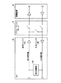
【解決手段】 被試験デバイスを試験する試験装置であって、被試験デバイスから出力される信号を受信して、第1基準電圧と比較して論理信号に変換するコンパレータと、被試験デバイスに対して出力する論理信号を第2基準電圧に基づいて増幅し、被試験デバイスへ出力するドライバと、被試験デバイスから受信した受信信号の遅延量を補償するべく、第1基準電圧を決定し、コンパレータに設定するコンパレータ設定部と、コンパレータに設定した基準電圧に基づいて、ドライバに設定する第2基準電圧を決定し、ドライバに設定するドライバ設定部とを備える試験装置を提供する。
【選択図】図1
Description
現時点で先行公知文献の存在を確認していないので、先行公知文献に関する記載を省略する。
また、ドライバは、コンパレータにより変換された論理信号を、第2基準電圧に基づいて増幅し、被試験デバイスへ出力してもよい。
また、ドライバ設定部は、コンパレータ設定部が第1基準電圧を変更前の電圧と比較してより低い電圧に低下させた場合に、第2基準電圧を変更前の電圧と比較してより高い電圧に上昇させてもよい。
また、送信側イコライザは、受信側イコライザにより増幅された信号を更に増幅し、被試験デバイスへ送信してもよい。
また、送信側イコライザ設定部は、受信側イコライザ設定部が予め定められた周波数成分を増幅させる増幅量を増加させた場合に、被試験デバイスに送信する送信信号の増幅量を増加させてもよい。
なお、上記の発明の概要は、本発明の必要な特徴の全てを列挙したものではなく、これらの特徴群のサブコンビネーションもまた、発明となりうる。
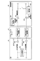
15 パフォーマンスボード
20 試験装置
100 自己試験部
110 出力バッファ
120 入力バッファ
200 コンパレータ
210 ドライバ
220 コンパレータ設定部
230 ドライバ設定部
240 受信側イコライザ
250 送信側イコライザ
260 受信側イコライザ設定部
270 送信側イコライザ設定部
Claims (8)
- 被試験デバイスを試験する試験装置であって、
前記被試験デバイスから出力される信号を受信して、第1基準電圧と比較して論理信号に変換するコンパレータと、
前記被試験デバイスに対して出力する論理信号を第2基準電圧に基づいて増幅し、前記被試験デバイスへ出力するドライバと、
前記被試験デバイスから受信した受信信号の遅延量を補償するべく、前記第1基準電圧を決定し、前記コンパレータに設定するコンパレータ設定部と、
前記コンパレータに設定した基準電圧に基づいて、前記ドライバに設定する前記第2基準電圧を決定し、前記ドライバに設定するドライバ設定部と
を備える試験装置。 - 前記ドライバは、前記コンパレータにより変換された前記論理信号を、前記第2基準電圧に基づいて増幅し、前記被試験デバイスへ出力する
請求項1記載の試験装置。 - 前記ドライバ設定部は、前記コンパレータ設定部が前記第1基準電圧を変更前の電圧と比較してより低い電圧に低下させた場合に、前記第2基準電圧を変更前の電圧と比較してより高い電圧に上昇させる
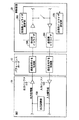
請求項1記載の試験装置。 - 周波数成分毎に増幅量を設定可能なイコライザを有し、被試験デバイスを試験する試験装置であって、
前記被試験デバイスから出力される信号を受信して増幅する受信側イコライザと、
前記被試験デバイスに出力するべき信号を増幅して送信する送信側イコライザと、
前記被試験デバイスから受信した受信信号の遅延量を補償するべく、前記受信信号の予め定められた周波数成分を前記受信側イコライザにより増幅させる増幅量を決定し、前記受信側イコライザに設定する受信側イコライザ設定部と、
前記被試験デバイスに送信する送信信号の前記予め定められた周波数成分を前記送信側イコライザにより増幅させる増幅量を、前記受信側イコライザ設定部が設定した前記増幅量に基づいて決定し、前記送信側イコライザに設定する送信側イコライザ設定部と
を備える試験装置。 - 前記送信側イコライザは、前記受信側イコライザにより増幅された信号を更に増幅し、前記被試験デバイスへ送信する
請求項4記載の試験装置。 - 前記送信側イコライザ設定部は、前記受信側イコライザ設定部が前記予め定められた周波数成分を増幅させる増幅量を増加させた場合に、前記被試験デバイスに送信する送信信号の増幅量を増加させる
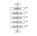
請求項4記載の試験装置。 - 被試験デバイスを試験する試験装置の設定方法であって、
前記試験装置は、
前記被試験デバイスから出力される信号を受信して、第1基準電圧と比較して論理信号に変換するコンパレータと、
前記被試験デバイスに対して出力する論理信号を第2基準電圧に基づいて増幅し、前記被試験デバイスへ出力するドライバと
を有し、
前記被試験デバイスから受信した受信信号の遅延量を補償するべく、前記第1基準電圧を決定し、前記コンパレータに設定するコンパレータ設定段階と、
前記コンパレータに設定した基準電圧に基づいて、前記ドライバに設定する前記第2基準電圧を決定し、前記ドライバに設定するドライバ設定段階と
を備えた設定方法。 - 周波数成分毎に増幅量を設定可能なイコライザを有し、被試験デバイスを試験する試験装置の設定方法であって、
前記試験装置は、
前記被試験デバイスから出力される信号を受信して増幅する受信側イコライザと、
前記被試験デバイスに出力するべき信号を増幅して送信する送信側イコライザと、
を有し、
前記被試験デバイスから受信した受信信号の遅延量を補償するべく、前記受信信号の予め定められた周波数成分を前記受信側イコライザにより増幅させる増幅量を決定し、前記受信側イコライザに設定する受信側イコライザ設定段階と、
前記被試験デバイスに送信する送信信号の前記予め定められた周波数成分を前記送信側イコライザにより増幅させる増幅量を、前記受信側イコライザ設定段階において設定された前記増幅量に基づいて決定し、前記送信側イコライザに設定する送信側イコライザ設定段階と
を備えた設定方法。
Priority Applications (2)
| Application Number | Priority Date | Filing Date | Title |
|---|---|---|---|
| JP2004109297A JP4197657B2 (ja) | 2004-04-01 | 2004-04-01 | 試験装置及び設定方法 |
| US11/094,325 US7453932B2 (en) | 2004-04-01 | 2005-03-30 | Test device and setting method |
Applications Claiming Priority (1)
| Application Number | Priority Date | Filing Date | Title |
|---|---|---|---|
| JP2004109297A JP4197657B2 (ja) | 2004-04-01 | 2004-04-01 | 試験装置及び設定方法 |
Publications (2)
| Publication Number | Publication Date |
|---|---|
| JP2005292004A true JP2005292004A (ja) | 2005-10-20 |
| JP4197657B2 JP4197657B2 (ja) | 2008-12-17 |
Family
ID=35187075
Family Applications (1)
| Application Number | Title | Priority Date | Filing Date |
|---|---|---|---|
| JP2004109297A Expired - Fee Related JP4197657B2 (ja) | 2004-04-01 | 2004-04-01 | 試験装置及び設定方法 |
Country Status (2)
| Country | Link |
|---|---|
| US (1) | US7453932B2 (ja) |
| JP (1) | JP4197657B2 (ja) |
Cited By (2)
| Publication number | Priority date | Publication date | Assignee | Title |
|---|---|---|---|---|
| US7801211B2 (en) | 2007-06-15 | 2010-09-21 | Advantest Corporation | Communication system, receiver unit, and adaptive equalizer |
| US8610449B2 (en) | 2008-06-02 | 2013-12-17 | Advantest Corporation | Wafer unit for testing and test system |
Families Citing this family (4)
| Publication number | Priority date | Publication date | Assignee | Title |
|---|---|---|---|---|
| JP5182859B2 (ja) * | 2007-01-29 | 2013-04-17 | 株式会社ステップテクニカ | 評価装置及び評価システム |
| KR20120137963A (ko) * | 2011-06-14 | 2012-12-24 | 삼성전자주식회사 | 신호전송장치 및 이를 이용한 반도체 테스트 장치 |
| US11164551B2 (en) | 2019-02-28 | 2021-11-02 | Clifford W. Chase | Amplifier matching in a digital amplifier modeling system |
| KR102902641B1 (ko) | 2021-08-11 | 2025-12-23 | 삼성전자주식회사 | 이미지 센서를 테스트하기 인터페이스 보드, 그것을 갖는 테스트 시스템, 및 그것의 동작 방법 |
Family Cites Families (5)
| Publication number | Priority date | Publication date | Assignee | Title |
|---|---|---|---|---|
| JP2866750B2 (ja) * | 1991-01-28 | 1999-03-08 | 三菱電機株式会社 | 半導体試験装置および半導体装置の試験方法 |
| EP0872961B1 (en) * | 1998-01-15 | 2000-03-29 | Hewlett-Packard Company | Attenuation equalizer for transmission lines |
| US6133725A (en) * | 1998-03-26 | 2000-10-17 | Teradyne, Inc. | Compensating for the effects of round-trip delay in automatic test equipment |
| US6360180B1 (en) * | 1999-05-10 | 2002-03-19 | Teradyne, Inc. | Driver with transmission path loss compensation |
| US20040187049A1 (en) * | 2003-02-27 | 2004-09-23 | Nptest, Inc. | Very small pin count IC tester |
-
2004
- 2004-04-01 JP JP2004109297A patent/JP4197657B2/ja not_active Expired - Fee Related
-
2005
- 2005-03-30 US US11/094,325 patent/US7453932B2/en active Active
Cited By (2)
| Publication number | Priority date | Publication date | Assignee | Title |
|---|---|---|---|---|
| US7801211B2 (en) | 2007-06-15 | 2010-09-21 | Advantest Corporation | Communication system, receiver unit, and adaptive equalizer |
| US8610449B2 (en) | 2008-06-02 | 2013-12-17 | Advantest Corporation | Wafer unit for testing and test system |
Also Published As
| Publication number | Publication date |
|---|---|
| US20050243906A1 (en) | 2005-11-03 |
| US7453932B2 (en) | 2008-11-18 |
| JP4197657B2 (ja) | 2008-12-17 |
Similar Documents
| Publication | Publication Date | Title |
|---|---|---|
| JP5095613B2 (ja) | データパケット信号受信機の感度を計測するための方法 | |
| CN102790039B (zh) | 半导体芯片以及半导体芯片的检查方法 | |
| US8610449B2 (en) | Wafer unit for testing and test system | |
| CN102016614A (zh) | 选择性地使用或绕过远程管脚电子设备块来测试至少一个待测设备的方法和装置 | |
| CN111415701B (zh) | 眼图生成装置及方法、存储芯片测试系统 | |
| US6631486B1 (en) | Semiconductor integrated circuit and method for testing the same | |
| JP2010038581A (ja) | 半導体試験装置 | |
| EP2667518A1 (en) | Receiving apparatus for test signal, electronic apparatus therefor and signal receiving method thereof | |
| JP4197657B2 (ja) | 試験装置及び設定方法 | |
| WO2008081347A1 (en) | Method for testing a variable digital delay line and a device having variable digital delay line testing capabilities | |
| CN108614206B (zh) | 一种芯片测试装置、测试方法及测试板 | |
| US10079701B1 (en) | Three-valued signal generation device and three-valued signal generation method | |
| US7667554B2 (en) | Pre-emphasis adjustment method | |
| US20060170517A1 (en) | Signal transfer system, signal output circuit board, signal receiving circuit board, signal output method, and signal receiving method | |
| JP2009302613A (ja) | 波形生成回路 | |
| JP2016063430A (ja) | 送受信回路、集積回路及び試験方法 | |
| TWI674423B (zh) | 系統芯片、以及其內建自我測試電路與自我測試方法 | |
| US6381722B1 (en) | Method and apparatus for testing high speed input paths | |
| JPWO2009014072A1 (ja) | 誤差要因測定装置、方法、プログラム、記録媒体および該装置を備えた出力補正装置、反射係数測定装置 | |
| KR20120137963A (ko) | 신호전송장치 및 이를 이용한 반도체 테스트 장치 | |
| CN111025132B (zh) | 系统芯片、以及其内建自我测试电路与自我测试方法 | |
| JP2009047480A (ja) | 半導体試験装置 | |
| US7902856B2 (en) | Semiconductor integrated circuit | |
| US20250085335A1 (en) | Testing apparatus | |
| EP2533062A1 (en) | A radio frequency integrated circuit |
Legal Events
| Date | Code | Title | Description |
|---|---|---|---|
| A621 | Written request for application examination |
Free format text: JAPANESE INTERMEDIATE CODE: A621 Effective date: 20070223 |
|
| A977 | Report on retrieval |
Free format text: JAPANESE INTERMEDIATE CODE: A971007 Effective date: 20080717 |
|
| A131 | Notification of reasons for refusal |
Free format text: JAPANESE INTERMEDIATE CODE: A131 Effective date: 20080805 |
|
| A521 | Request for written amendment filed |
Free format text: JAPANESE INTERMEDIATE CODE: A523 Effective date: 20080828 |
|
| TRDD | Decision of grant or rejection written | ||
| A01 | Written decision to grant a patent or to grant a registration (utility model) |
Free format text: JAPANESE INTERMEDIATE CODE: A01 Effective date: 20080924 |
|
| A01 | Written decision to grant a patent or to grant a registration (utility model) |
Free format text: JAPANESE INTERMEDIATE CODE: A01 |
|
| A61 | First payment of annual fees (during grant procedure) |
Free format text: JAPANESE INTERMEDIATE CODE: A61 Effective date: 20080929 |
|
| FPAY | Renewal fee payment (event date is renewal date of database) |
Free format text: PAYMENT UNTIL: 20111010 Year of fee payment: 3 |
|
| R150 | Certificate of patent or registration of utility model |
Free format text: JAPANESE INTERMEDIATE CODE: R150 |
|
| FPAY | Renewal fee payment (event date is renewal date of database) |
Free format text: PAYMENT UNTIL: 20121010 Year of fee payment: 4 |
|
| FPAY | Renewal fee payment (event date is renewal date of database) |
Free format text: PAYMENT UNTIL: 20131010 Year of fee payment: 5 |
|
| R250 | Receipt of annual fees |
Free format text: JAPANESE INTERMEDIATE CODE: R250 |
|
| R250 | Receipt of annual fees |
Free format text: JAPANESE INTERMEDIATE CODE: R250 |
|
| LAPS | Cancellation because of no payment of annual fees |