JP2005243738A - Accommodating light-emitting device and package therefor - Google Patents
Accommodating light-emitting device and package therefor Download PDFInfo
- Publication number
- JP2005243738A JP2005243738A JP2004048560A JP2004048560A JP2005243738A JP 2005243738 A JP2005243738 A JP 2005243738A JP 2004048560 A JP2004048560 A JP 2004048560A JP 2004048560 A JP2004048560 A JP 2004048560A JP 2005243738 A JP2005243738 A JP 2005243738A
- Authority
- JP
- Japan
- Prior art keywords
- emitting element
- light emitting
- light
- recess
- frame body
- Prior art date
- Legal status (The legal status is an assumption and is not a legal conclusion. Google has not performed a legal analysis and makes no representation as to the accuracy of the status listed.)
- Pending
Links
Images


Classifications
-
- H—ELECTRICITY
- H01—ELECTRIC ELEMENTS
- H01L—SEMICONDUCTOR DEVICES NOT COVERED BY CLASS H10
- H01L2224/00—Indexing scheme for arrangements for connecting or disconnecting semiconductor or solid-state bodies and methods related thereto as covered by H01L24/00
- H01L2224/01—Means for bonding being attached to, or being formed on, the surface to be connected, e.g. chip-to-package, die-attach, "first-level" interconnects; Manufacturing methods related thereto
- H01L2224/42—Wire connectors; Manufacturing methods related thereto
- H01L2224/47—Structure, shape, material or disposition of the wire connectors after the connecting process
- H01L2224/48—Structure, shape, material or disposition of the wire connectors after the connecting process of an individual wire connector
- H01L2224/4805—Shape
- H01L2224/4809—Loop shape
- H01L2224/48091—Arched
-
- H—ELECTRICITY
- H01—ELECTRIC ELEMENTS
- H01L—SEMICONDUCTOR DEVICES NOT COVERED BY CLASS H10
- H01L2224/00—Indexing scheme for arrangements for connecting or disconnecting semiconductor or solid-state bodies and methods related thereto as covered by H01L24/00
- H01L2224/01—Means for bonding being attached to, or being formed on, the surface to be connected, e.g. chip-to-package, die-attach, "first-level" interconnects; Manufacturing methods related thereto
- H01L2224/42—Wire connectors; Manufacturing methods related thereto
- H01L2224/47—Structure, shape, material or disposition of the wire connectors after the connecting process
- H01L2224/48—Structure, shape, material or disposition of the wire connectors after the connecting process of an individual wire connector
- H01L2224/481—Disposition
- H01L2224/48151—Connecting between a semiconductor or solid-state body and an item not being a semiconductor or solid-state body, e.g. chip-to-substrate, chip-to-passive
- H01L2224/48221—Connecting between a semiconductor or solid-state body and an item not being a semiconductor or solid-state body, e.g. chip-to-substrate, chip-to-passive the body and the item being stacked
- H01L2224/48225—Connecting between a semiconductor or solid-state body and an item not being a semiconductor or solid-state body, e.g. chip-to-substrate, chip-to-passive the body and the item being stacked the item being non-metallic, e.g. insulating substrate with or without metallisation
- H01L2224/48227—Connecting between a semiconductor or solid-state body and an item not being a semiconductor or solid-state body, e.g. chip-to-substrate, chip-to-passive the body and the item being stacked the item being non-metallic, e.g. insulating substrate with or without metallisation connecting the wire to a bond pad of the item
Abstract
Description
本発明は、発光ダイオード等の発光素子を用いた表示装置等に用いられる、発光素子を収納するための発光素子収納用パッケージおよび発光装置に関する。 The present invention relates to a light-emitting element storage package and a light-emitting device for storing a light-emitting element, which are used in a display device using a light-emitting element such as a light-emitting diode.
従来、発光ダイオード等の発光素子を収納するための発光素子収納用パッケージ(以下、パッケージともいう)として、セラミックス製のパッケージが用いられており、その一例を図10に示す(例えば、下記の特許文献1参照)。同図に示すように、従来のパッケージは、上面に凹部14が形成されているとともに凹部14の底面に発光素子13を搭載するための導体層から成る搭載部12が設けられた、複数のセラミック層が積層されて成る直方体状の絶縁基体11と、絶縁基体11の搭載部12およびその周辺から絶縁基体11の下面にかけて形成された一対の配線導体15とから主に構成されている。また、絶縁基体11の凹部14の内周面は、光を外部に良好に放射させるため、凹部14の底面から絶縁基体11の上面にかけて外側に広がるように形成されている。
Conventionally, a ceramic package has been used as a light-emitting element storage package (hereinafter also referred to as a package) for storing light-emitting elements such as light-emitting diodes, and an example thereof is shown in FIG. Reference 1). As shown in the figure, the conventional package has a plurality of ceramics in which a
そして、一方の配線導体15の一端が電気的に接続された搭載部12上に発光素子13を導電性接着剤、半田等を介して載置固定するとともに電気的に接続し、発光素子13の電極と他方の配線導体15とをボンディングワイヤ16を介して電気的に接続し、しかる後、絶縁基体11の凹部14内に図示しない透明樹脂を充填して発光素子13を封止することによって、発光装置が作製される。
Then, the
また、凹部14の内周面で発光素子13の光を反射させてパッケージの上方に光を放射させるために、凹部14の内周面にニッケル(Ni)めっき層や金(Au)めっき層を表面に有するメタライズ層からなる金属層17を被着させていることもある。
Further, in order to reflect the light of the
上記のパッケージはセラミックグリーンシート積層法により以下のようにして製作される。まず、絶縁基体11の搭載部12が位置する平面より下側の部位を形成するためのセラミックグリーンシート(以下、グリーンシートAという)と、絶縁基体11の凹部14の側壁を形成するためのセラミックグリーンシート(以下、グリーンシートBという)とを準備し、これらのグリーンシートA,Bに配線導体15を導出させるための貫通孔や凹部14となる貫通穴を打ち抜き法で形成する。
The above package is manufactured by the ceramic green sheet lamination method as follows. First, a ceramic green sheet (hereinafter referred to as green sheet A) for forming a portion below the plane on which the
次に、グリーンシートAの貫通孔および所定の部位に、メタライズ層から成る配線導体15形成用の導体ペーストをスクリーン印刷法等で印刷塗布し、また、グリーンシートBの凹部14となる貫通穴の内周面に金属層17形成用の導体ペーストをスクリーン印刷法等で印刷塗布する。
Next, a conductive paste for forming a
次に、グリーンシートAとグリーンシートBとを重ねて接着して絶縁基体11を形成するための積層体とし、これを所定寸法に切断して成形体となし、高温(1600℃程度)で焼成して焼結体となす。その後、配線導体15および金属層17の露出表面にニッケル,金,パラジウム,白金等の金属から成るめっき金属層を無電解めっき法や電解めっき法により被着させることによって、パッケージが製作される。
しかしながら、上記従来のパッケージにおいては、凹部14の内周面が凹部14の底面から絶縁基体の上面に向かうに伴って外側に広がるように形成されているため、凹部14の内周面の上面の開口より、発光素子13が発光する光が広範囲にわたって放射され易く、発光素子13の光の正面方向への指向性が低くなるという問題点があった。そのため、正面方向の輝度が低くなるとともに、凹部14の開口付近の輪郭がぼやけ、正面方向からの視認性が低下するという問題点を有していた。
However, in the above conventional package, the inner peripheral surface of the
従って、本発明は上記従来の問題点に鑑みて完成されたものであり、その目的は、発光素子が発光する光を効率良く放射することができるとともに、視認性の高いものとすることができる発光素子収納用パッケージおよび発光装置を提供することにある。 Therefore, the present invention has been completed in view of the above-described conventional problems, and an object of the present invention is to efficiently emit light emitted from the light emitting element and to achieve high visibility. It is an object to provide a light emitting element storage package and a light emitting device.
本発明の発光素子収納用パッケージは、上面に発光素子を収容するための凹部を有するとともに該凹部の底面の中央部に前記発光素子の搭載部が形成された絶縁基体と、前記凹部の底面に形成された、前記発光素子の電極が電気的に接続される配線導体とを具備しており、前記凹部の内側面に、下側開口から上側開口に向かうに伴って内寸法が漸次小さくなるとともに内周面が内側に凸とされた枠体が嵌着されていることを特徴とする。 The light emitting element storage package of the present invention includes an insulating base having a recess for receiving the light emitting element on the top surface and a mounting portion of the light emitting element formed at the center of the bottom surface of the recess, and a bottom surface of the recess. And a wiring conductor to which the electrode of the light emitting element is electrically connected. The inner dimension of the inner surface of the recess gradually decreases from the lower opening toward the upper opening. A frame body having an inner peripheral surface protruding inward is fitted.
本発明の発光素子収納用パッケージにおいて、好ましくは、前記絶縁基体は、前記凹部の底面の露出した部位が光反射面とされていることを特徴とする。 In the light emitting element storage package according to the present invention, preferably, the insulating base is characterized in that the exposed portion of the bottom surface of the recess is a light reflecting surface.
本発明の発光素子収納用パッケージにおいて、好ましくは、前記枠体は、上側の開口縁が平面視で前記発光素子の外周と合致しているかまたは外周よりも内側にあることを特徴とする。 In the light emitting element storage package of the present invention, it is preferable that the frame body has an upper opening edge that coincides with an outer periphery of the light emitting element in a plan view or is on an inner side of the outer periphery.
本発明の発光素子収納用パッケージにおいて、好ましくは、前記枠体は、アルミニウム,銀,金,パラジウムおよび白金の少なくとも一つを主成分とすることを特徴とする。 In the light emitting element storage package according to the present invention, it is preferable that the frame body contains at least one of aluminum, silver, gold, palladium, and platinum as a main component.
本発明の発光素子収納用パッケージにおいて、好ましくは、前記枠体は、前記内周面にアルミニウム,銀,金,パラジウムおよび白金の少なくとも一つを主成分とする金属層が被着されていることを特徴とする。 In the light emitting element storage package according to the present invention, preferably, the frame body has a metal layer mainly composed of at least one of aluminum, silver, gold, palladium and platinum attached to the inner peripheral surface. It is characterized by.
本発明の発光装置は、上記本発明の発光素子収納用パッケージと、前記搭載部に搭載されるとともに前記配線導体に電気的に接続された発光素子と、該発光素子を覆う透光性部材とを具備していることを特徴とする。 The light emitting device of the present invention includes a light emitting element storage package according to the present invention, a light emitting element mounted on the mounting portion and electrically connected to the wiring conductor, and a translucent member covering the light emitting element. It is characterized by comprising.
本発明の発光素子収納用パッケージは、凹部の内側面に、前記凹部の内側面に、下側開口から上側開口に向かうに伴って内寸法が漸次小さくなるとともに内周面が内側に凸とされた枠体が嵌着されていることから、発光素子から真上方向に発光される光を枠体の上側開口から良好に放射することができるとともに、発光素子から小さな放射角度で発光された、真上方向よりも多少斜め上方向に進む光を、枠体の上側の内周面に対して入射角の小さい光として反射させることによって真上方向に集約して放射することができる。さらに、発光素子から大きな放射角度で発光された、真上方向対して斜めに大きな角度で進む光を、枠体の内周面で反射させて枠体の内側に閉じ込め、枠体の上側の開口より真上方向に非常に小さい放射角度で進む光のみを枠体の外側に放射させて高密度に光を集約することができる。その結果、光が集約された方向に対する輝度も向上するとともに、枠体上側の開口の輪郭が明るく鮮明になり、視認性の高いものとなる。 In the light emitting element storage package of the present invention, the inner dimension gradually decreases from the lower opening toward the upper opening on the inner surface of the recess, and the inner peripheral surface protrudes inward on the inner surface of the recess. Since the frame is fitted, the light emitted from the light emitting element in the upward direction can be radiated well from the upper opening of the frame, and emitted from the light emitting element at a small radiation angle. By reflecting light traveling in a slightly obliquely upward direction from the directly upward direction as light having a small incident angle with respect to the inner peripheral surface on the upper side of the frame body, the light can be concentrated and emitted in the upward direction. Further, light emitted from the light emitting element at a large radiation angle and traveling at a large angle obliquely with respect to the upward direction is reflected by the inner peripheral surface of the frame body and confined inside the frame body, and the upper opening of the frame body Only light traveling at a very small radiation angle in the upward direction can be radiated to the outside of the frame to concentrate the light at high density. As a result, the luminance with respect to the direction in which the light is concentrated is improved, the outline of the opening on the upper side of the frame is bright and clear, and the visibility is high.
また、斜め上方に発光された光が枠体で遮られた後、凹部の内側で枠体と絶縁基体との間で高い反射率で反射が繰り変えされて枠体の内側に光がある程度閉じ込められ、放射角度が搭載部に対して直角に近くなったところで枠体の上側の開口より正面方向に放射することができる。よって、光の漏れや減衰を抑えることができるとともに発光素子から発光された光をきわめて効率よく放射でき、指向性および放射光強度が高いものとすることができる。 In addition, after the light emitted obliquely upward is blocked by the frame body, reflection is repeated between the frame body and the insulating base at a high reflectance inside the recess, and the light is confined to some extent inside the frame body. When the radiation angle is close to a right angle with respect to the mounting portion, the radiation can be emitted in the front direction from the upper opening of the frame. Therefore, leakage and attenuation of light can be suppressed, light emitted from the light emitting element can be radiated very efficiently, and directivity and radiated light intensity can be increased.
また、下側開口から上側開口に向かうに伴って内寸法が漸次小さくなるので、発光素子の搭載部を広く形成し、大きな発光素子を搭載したり、複数の発光素子を搭載することができるので、より輝度が高く集約したものとすることができる。 In addition, since the inner dimension gradually decreases from the lower opening toward the upper opening, the light emitting element mounting portion can be formed wide, and a large light emitting element or a plurality of light emitting elements can be mounted. , The luminance can be higher and aggregated.
本発明の発光素子収納用パッケージは、好ましくは、絶縁基体の凹部の底面の露出した部位が光反射面とされていることから、発光素子から発光された光や枠体の内周面で反射された光を低損失で反射させることができ、発光効率の優れたものとすることができる。 In the light emitting element storage package of the present invention, preferably, the exposed portion of the bottom surface of the concave portion of the insulating base is a light reflecting surface, so that the light emitted from the light emitting element or the inner peripheral surface of the frame is reflected. The reflected light can be reflected with low loss, and the light emission efficiency can be improved.
本発明の発光素子収納用パッケージは、好ましくは、枠体の上側の開口縁が平面視で発光素子の外周と合致しているかまたは外周よりも内側にあることから、発光素子から発光される光のうち斜め上方の光をより効果的に遮断することができ、より指向性の高いものとすることができる。 In the light emitting element storage package of the present invention, it is preferable that the opening edge on the upper side of the frame body coincides with the outer periphery of the light emitting element in a plan view or is on the inner side of the outer periphery. Among them, it is possible to block light obliquely upward more effectively, and to have higher directivity.
本発明の発光素子収納用パッケージは、好ましくは、枠体は、アルミニウム,銀,金,パラジウムおよび白金の少なくとも一つを主成分とすることから、発光素子から斜め上方に発光される光を枠体でより良好に反射させることができ、枠体の内側に閉じ込められて枠体と絶縁基体との間で反射を繰り返す際の光損失を有効に抑制し、発光効率の高いものとすることができる。 In the light emitting element storage package according to the present invention, preferably, the frame body mainly includes at least one of aluminum, silver, gold, palladium, and platinum, so that light emitted obliquely upward from the light emitting element is framed. It can be reflected better by the body, and it is confined inside the frame body, effectively suppressing light loss when repeatedly reflecting between the frame body and the insulating substrate, and having high luminous efficiency. it can.
本発明の発光素子収納用パッケージは、好ましくは、枠体は、内周面にアルミニウム,銀,金,パラジウムおよび白金の少なくとも一つを主成分とする金属層が被着されていることから、枠体の材質を絶縁基体との間で熱膨張係数差などによる応力が生じ難いもので構成でき、発光素子収納用パッケージに破損などが生じるのを有効に防止できるとともに、発光素子から斜め上方に発光される光を金属層でより良好に反射させることができ、枠体の内側に閉じ込められて金属層と絶縁基体との間で反射を繰り返す際の光損失を有効に抑制し、発光効率の高いものとすることができる。 In the light emitting element storage package of the present invention, preferably, the frame body has a metal layer mainly composed of at least one of aluminum, silver, gold, palladium and platinum attached to the inner peripheral surface. The frame material can be made of a material that does not easily generate stress due to the difference in thermal expansion coefficient between the insulating base and the light emitting element storage package, and can be effectively prevented from being damaged, and obliquely upward from the light emitting element. The emitted light can be reflected better by the metal layer, and it is confined inside the frame and effectively suppresses light loss when it is repeatedly reflected between the metal layer and the insulating substrate, thereby improving the luminous efficiency. Can be expensive.
本発明の発光装置は、上記本発明の発光素子収納用パッケージと、搭載部に搭載されるとともに配線導体に電気的に接続された発光素子と、発光素子を覆う透光性部材とを具備していることから、上記本発明の発光素子収納用パッケージの特徴を有する、発光素子が発光する光を効率良く放射することができるとともに、視認性の高いものとすることができる。従って、表示装置等に好適なものとなる。 A light-emitting device of the present invention includes the above-described light-emitting element storage package of the present invention, a light-emitting element mounted on the mounting portion and electrically connected to the wiring conductor, and a translucent member that covers the light-emitting element. Therefore, the light emitted from the light-emitting element, which has the characteristics of the light-emitting element storage package of the present invention, can be efficiently emitted and can be highly visible. Therefore, it is suitable for a display device or the like.
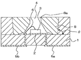
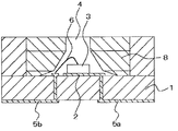
本発明の発光素子収納用パッケージを以下に詳細に説明する。図1は本発明のパッケージについて実施の形態の一例を示す断面図であり、図2は図1におけるパッケージの平面図であり、これらの図において、1は絶縁基体、2は発光素子3の搭載部、3は発光素子、4は発光素子3を収容するための凹部、8は枠体である。
The light emitting element storage package of the present invention will be described in detail below. 1 is a cross-sectional view showing an example of an embodiment of the package of the present invention. FIG. 2 is a plan view of the package in FIG. 1. In these drawings, 1 is an insulating substrate, 2 is a light-emitting
本発明のパッケージは、上面に発光素子3を収容するための凹部4を有するとともに凹部4の底面の中央部に発光素子3の搭載部2が形成された絶縁基体1と、凹部4の底面に形成された、発光素子3の電極が電気的に接続される配線導体5a,5bとを具備しており、凹部4の内側面に、下側開口から上側開口に向かうに伴って内寸法が漸次小さくなるとともに内周面が内側に凸とされた枠体8が嵌着されている。
The package of the present invention has an
本発明の絶縁基体1はセラミックスや樹脂から成り、セラミックスからなる場合、例えば酸化アルミニウム質焼結体(アルミナセラミックス),窒化アルミニウム質焼結体,ムライト質焼結体,ガラスセラミックス等のセラミックスから成る絶縁層を複数層積層してなる直方体状の箱状体であり、上面の中央部に発光素子3を収容するための凹部4が形成されている。絶縁基体1が例えば酸化アルミニウム質焼結体から成る場合、酸化アルミニウム、酸化珪素、酸化マグネシウム、酸化カルシウム等の原料粉末に適当な有機バインダー、溶剤等を添加混合して泥漿状となし、これを従来周知のドクターブレード法やカレンダーロール法等によりシート状に成形してセラミックグリーンシート(セラミック生シート)を得、しかる後、セラミックグリーンシートに凹部4用の貫通孔を打ち抜き加工で形成するとともに、発光素子3を搭載するためのセラミックグリーンシートと凹部4の側壁用のセラミックグリーンシートとを複数枚積層し、高温(約1600℃)にて焼成し、一体化することで形成される。
The insulating
また、凹部4の底面には発光素子3を搭載するための導体層から成る搭載部2が形成されており、搭載部2はタングステン(W),モリブデン(Mo),銅(Cu),銀(Ag)等の金属粉末のメタライズ層から成っている。
A mounting
また、絶縁基体1は、搭載部2およびその周辺から絶縁基体1の下面にかけて形成された配線導体5a,5bが被着形成されている。配線導体5a,5bは、WやMo等の金属粉末のメタライズ層から成り、凹部4に収容された発光素子3を外部に電気的に接続するための導電路である。そして、搭載部2には発光ダイオード(LED),半導体レーザ(LD)等の発光素子3が金(Au)−シリコン(Si)合金やAg−エポキシ樹脂等の導電性接合材により固着されるとともに、配線導体5bには発光素子3の電極がボンディングワイヤ6等を介して電気的に接続されている。そして、絶縁基体1下面の配線導体5a,5bが外部電気回路基板の配線導体に接続されることで発光素子3の各電極と電気的に接続され、発光素子3へ電力や駆動信号が供給される。また、発光素子3は搭載部2および配線導体5bにフリップチップ実装により接続されても構わない。
In addition, the insulating
配線導体5a,5bは、例えばWやMo等の金属粉末に適当な有機溶剤、溶媒を添加混合して得た金属ペーストを絶縁基体1となるグリーンシートに予めスクリーン印刷法により所定パターンに印刷塗布しておくことによって、絶縁基体1の所定位置に被着形成される。
For the
なお、配線導体5a,5bおよび搭載部2の露出する表面に、ニッケル(Ni),金(Au),Ag等の耐蝕性に優れる金属を1〜20μm程度の厚みで被着させておくのがよく、配線導体5a,5bおよび搭載部2が酸化腐蝕するのを有効に防止できるとともに、搭載部2と発光素子3との固着および配線導体5bとボンディングワイヤ6との接合、配線導体5a,5bと外部電気回路基板の配線導体との接合を強固にすることができる。従って、配線導体5a,5bおよび搭載部2の露出表面には、厚さ1〜10μm程度のNiめっき層と厚さ0.1〜3μm程度のAuめっき層またはAgめっき層とが、電解めっき法や無電解めっき法により順次被着されていることがより好ましい。
It is to be noted that a metal having excellent corrosion resistance such as nickel (Ni), gold (Au), Ag or the like is deposited on the exposed surfaces of the
そして、本発明において、凹部4の内側面に、下側開口から上側開口に向かうに伴って内寸法が漸次小さくなるとともに内周面が内側に凸とされた枠体8が嵌着されている。これにより、発光素子3から真上方向に発光される光を枠体8の上側開口から良好に放射することができるとともに、発光素子3から小さな放射角度で発光された、真上方向よりも多少斜め上方向に進む光を、枠体8の上側の内周面に対して入射角の小さい光として反射させることによって真上方向に集約して放射することができる。さらに、発光素子3から大きな放射角度で発光された、真上方向対して斜めに大きな角度で進む光を、枠体8の内周面で反射させて枠体8の内側に閉じ込め、枠体8の上側の開口より真上方向に非常に小さい放射角度で進む光のみを枠体8の外側に放射させて高密度に光を集約することができる。その結果、光が集約された方向に対する輝度も向上するとともに、枠体8上側の開口の輪郭が明るく鮮明になり、視認性の高いものとなる。
And in this invention, the
また、斜め上方に発光された光が枠体8で遮られた後、凹部4の内側で枠体8と絶縁基体1との間で高い反射率で反射が繰り変えされて枠体8の内側に光がある程度閉じ込められ、放射角度が搭載部2に対して直角に近くなったところで枠体8の上側の開口より正面方向に放射することができるので光の余計な漏れを抑えることができるとともに発光素子3から発光された光を効率よく放射できる。よって、光の漏れや減衰を抑えることができるとともに発光素子3から発光された光をきわめて効率よく放射でき、指向性および放射光強度が高いものとすることができる。
In addition, after light emitted obliquely upward is blocked by the
また、下側開口から上側開口に向かうに伴って内寸法が漸次小さくなるので、発光素子3の搭載部2を広く形成し、大きな発光素子3を搭載したり、複数の発光素子3を搭載することができるので、より輝度が高く集約したものとすることもできる。
Further, since the inner dimension gradually decreases from the lower opening toward the upper opening, the mounting
枠体8は、金属、セラミックス、樹脂、ガラス等が用いられ、内周面の光反射率を高めるために内周面に金属等の光反射率の高い光反射層が被着されていてもよい。好ましくは、枠体8は金属からなるのがよい。これにより、枠体8の内周面の表面状態を安定したものとしやすいとともに、発光素子3の発熱する熱を良好に外部に放射しやすいものとすることができる。
The
この枠体8は、樹脂接着剤により凹部4の内側面に嵌着され接着されていても良いし、凹部4の内側面に接合用のメタライズ層を形成し、Agろう等によりろう付けして接合されていても良い。また、凹部4内に発光素子3を収容し、ボンディングワイヤ6等を介して電気的接続を行った後に、凹部4内に枠体8を嵌着するとともに透明樹脂を封入し、透明樹脂で発光素子3を覆うとともに枠体8を固定することにより、枠体8を凹部4に接合させても良い。このような発光素子3を収容した後に枠体8を凹部4に嵌着する場合は、枠体8の上側の開口よりも発光素子3の大きさを大きくすることができ、これにより、発光素子3と配線導体5bとを電気的に接続するボンディングワイヤ6等を平面視で枠体8の上側の開口縁よりも外側に位置させることができるので、ボンディングワイヤ6で光が吸収されて強度むらが生じたり、ボンディングワイヤ6で光が屈接して指向性が低下したりするのを有効に防止でき、より高輝度で指向性の高いものとすることができる。
The
また、凹部4の底面や側壁の絶縁基体1が露出する部位に、蛍光材等を含有する樹脂を被着しておいても良く、光を凹部4内で良好に反射させることができるようになる。
In addition, a resin containing a fluorescent material or the like may be applied to the bottom surface of the
また、枠体8の開口縁や枠体8の上面、絶縁基体1の上面に暗色系のペースト等を被着させてもよく、これにより、正面方向から見た際に枠体8の開口縁や枠体8の上面、絶縁基体1の上面との明暗の区別を明確にし、正面から見た際の発光装置の視認性をより高めることができる。
Further, a dark-colored paste or the like may be applied to the opening edge of the
また、図3の断面図で示すように、枠体8の上側の開口縁を枠体8の内周面よりも狭くなるように、突出部8aを形成しても良い。これにより、枠体8の上側の開口より放射される光を、より集約して直上方向となるようにすることができる。
Further, as shown in the sectional view of FIG. 3, the protruding
また、枠体8が嵌着される凹部4は、横断面形状が円形状、長円形状、楕円形状、四角形状等であっても良い。また、図4の断面図で示すように、凹部4の内側面および枠体8の外周面を凹部4の底面から絶縁基体1の上面に向けて外側に広がるように若干の角度で傾斜させるのがよい。好ましくは、凹部4の底面から外側に延長した平面と凹部4の内側面との成す角度θが75〜85度であるのがよく、この場合、凹部4の内側面や上端部に若干の変形や反り等が発生したとしても、この変形や反り等に影響をあまり受けることなく、枠体8を容易に凹部4内に挿入することができる。
In addition, the
また、図2においては、横断面形状が円形状の凹部4に横断面形状が円形状の貫通穴が形成された枠体8が嵌着されているが、凹部4の横断面形状と枠体8の貫通穴の横断面形状は異なっていても良く、横断面形状が四角形状の凹部4に横断面形状が円形状の貫通穴が形成された枠体8を嵌着しても良いし、横断面形状が円形状の凹部4に横断面形状が四角形状の四角錐台形状の貫通穴が形成された枠体8を嵌着しても良い。
In FIG. 2, a
また、枠体8の上側と下側で反射層となる内周面の算術平均粗さを異ならせても良い。例えば、枠体8の上側の内周面の算術平均粗さを3μm以下とし、下側の内周面の算術平均粗さを3μm以上となるようにしても構わない。これにより、透明樹脂を枠体8の下側の内周面に強固に取着することができるとともに、内周面の上側で反射される光を枠体8の上側に向けやすくすることができる。また、内周面の下側で反射される光を散乱させて上側へ進む確率を大きくすることができる。
Further, the arithmetic average roughness of the inner peripheral surface serving as the reflective layer may be different between the upper side and the lower side of the
また、図5にパッケージの断面図で示すように、枠体8を複数の部位に分割して形成しておいても良く、枠体8の内周面の形状等を形成しやすく、枠体8の寸法精度を良好なものとして形成しやすくなる。
Further, as shown in the cross-sectional view of the package in FIG. 5, the
また、図6にパッケージの断面図で示すように、枠体8の内周面が弧形状の凸とされていても構わない。
Further, as shown in the sectional view of the package in FIG. 6, the inner peripheral surface of the
また、好ましくは、絶縁基体1の凹部4の底面の露出した部位が光反射面とされているのがよい。これにより、発光素子3から発光された光や枠体8の内周面で反射された光を低損失で反射させることができ、発光効率の優れたものとすることができる。このような光反射面は、絶縁基体1の上面にメタライズやめっき等で金属層を被着させたり、蛍光材を含有する樹脂等を塗布することにより形成することができる。なお、配線導体5a,5bのそれぞれが短絡しない程度に面積を大きくして配線導体5a,5bを光反射面としてもよい。あるいは、絶縁基体1を光反射率の高い材質、例えば、白色のアルミナセラミックスなどで構成することにより絶縁基体1の露出面を光反射面とすることができる。
Preferably, the exposed portion of the bottom surface of the
また、好ましくは、枠体8の上側の開口縁が平面視で発光素子3の外周と合致しているかまたは外周よりも内側にあるのがよい。これにより、発光素子3から発光される光のうち斜め上方の光をより効果的に遮断することができ、より指向性の高いものとすることができる。より好ましくは、枠体8の上側の開口形状は、平面視で発光素子3の外形と相似形にするのがよい。これにより、発光素子3から枠体8の上側開口から直接放出される光が多くなり、より発光強度が高いとともに指向性の高いものとすることができる。
Preferably, the opening edge on the upper side of the
また、枠体8は、好ましくは、アルミニウム,銀,金,パラジウムおよび白金の少なくとも一つを主成分とするのがよい。これにより、発光素子3から斜め上方に発光される光を枠体8でより良好に反射させることができ、枠体8の内側に閉じ込められて枠体8と絶縁基体1との間で反射を繰り返す際の光損失を有効に抑制し、発光効率の高いものとすることができる。特に、枠体8はアルミニウムから成るのがよく、この場合、枠体8が酸化腐食されにくいとともに、発光素子3の光波長の変動による光の反射率の変動も小さくなるので、広い用途に使用することができる。
The
また、絶縁基体1と枠体8との間に、絶縁基体1と枠体8との間に生じる応力を緩和させるために筒状の金属部材を介在させてもよい。好ましくは、この金属部材の熱膨張係数は、絶縁基体1の熱膨張係数と枠体8の熱膨張係数との間にあるのがよい。例えば、枠体8として、アルミニウム(熱膨張係数約23.5×10⁻⁶/℃程度),銀(熱膨張係数約19.1×10−6/℃程度),金(熱膨張係数約14.1×10−6/℃程度),パラジウム(熱膨張係数約11.8×10−6/℃程度)または白金(熱膨張係数約8.8×10−6/℃程度)を用い、絶縁基体1としてアルミナセラミックス(熱膨張係数7×10−6〜8×10−6/℃程度)等から成るものを用いる場合、絶縁基体1と枠体8との熱膨張係数差により発生する熱応力を緩和するために、絶縁基体1と枠体8との間にFe−Ni−Co合金(熱膨張係数6×10−6〜10×10−6/℃程度)、Cu−W合金(熱膨張係数6×10−6〜11×10−6/℃程度)等の金属部材を用いるのがよく、好ましくは、これらの枠体8の熱膨張係数と絶縁基体1の熱膨張係数との間の熱膨張係数となるFe−Ni−Co合金やCu−W合金を選択するのがよい。これにより、絶縁基体1と枠体8との熱膨張係数差により発生する熱応力を緩和して、枠体8の剥がれ等を有効に防止することができる。
A cylindrical metal member may be interposed between the insulating
なお、枠体8は、アルミニウム,銀,金,パラジウムまたは白金のいずれかを主成分とする合金であっても良い。
The
また、本発明における枠体8は、内周面にアルミニウム,銀,金,パラジウムおよび白金の少なくとも一つを主成分とする金属層8bが被着されていることが好ましい。これにより、枠体8の材質を絶縁基体1との間で熱膨張係数差などによる応力が生じ難いもので構成でき、発光素子収納用パッケージに破損などが生じるのを有効に防止できるとともに、発光素子3から斜め上方に発光される光を金属層8bでより良好に反射させることができ、枠体8の内側に閉じ込められて金属層8bと絶縁基体1との間で反射を繰り返す際の光損失を有効に抑制し、発光効率の高いものとすることができる。このような枠体8は、例えば図7に示すように、枠体8の内周面にアルミニウム,銀,金,パラジウムまたは白金のいずれかから成る金属層8bを被着したものである。特に、金属層8bはアルミニウムから成るのがよく、酸化腐食やマイグレーション等の不具合が発生しにくいとともに、発光素子3の光波長の変動による光の反射率の変動も小さくなるので、広い用途に使用することができる。
In the
また、枠体8として絶縁基体1に熱膨張係数の近い材質のものを使用するとよい。例えば、絶縁基体1としてアルミナセラミックス(熱膨張係数7×10⁻⁶〜8×10⁻⁶/℃程度)等から成るものを用い、枠体8として絶縁基体1に熱膨張係数の近いFe−Ni−Co合金(熱膨張係数6×10−6〜10×10−6/℃程度)等を使用すると、枠体8と絶縁基体1との剥がれ等を有効に防止することができる。このような材料から成る枠体8の内周面に金属層8bを被着すると、枠体8を絶縁基体1に強固に嵌着することができるとともに、発光素子3の発光する光に対する反射率を高いものとすることができる。
The
また、金属層8bは、枠体8の発光素子3側の表面(内周面)にのみ被着していても良いし、枠体8の全面に被着していてもよい。
In addition, the
なお、金属層8bはアルミニウム,銀,金,パラジウムまたは白金のいずれかを主成分とする合金層であっても良い。
Note that the
また、図8に示すように、本発明の発光素子収納用パッケージおよび発光装置をドットマトリックス状に配列させたものとすることで、表示装置として好適なものとして使用することもできる。また、枠体8の種類や金属層8bの種類を凹部4毎に異なるものとしても構わない。
In addition, as shown in FIG. 8, the light emitting element storage package and the light emitting device of the present invention are arranged in a dot matrix, so that it can be used as a suitable display device. Further, the type of the
本発明の発光装置は、本発明のパッケージと、搭載部2に搭載された発光素子3と、発光素子3を覆う透光性部材とを具備している。これにより、発光素子3が発光する光を良好に反射し、均一かつ効率良く外部に放射することができる、発光効率の高い高性能のものとなる。
The light emitting device of the present invention includes the package of the present invention, the
透光性部材はシリコーン等の透明樹脂、または、透明樹脂板やガラス板などが用いられる。透明樹脂の場合、透明樹脂は発光素子3およびその周囲のみを覆っていてもよいし、凹部4内に充填されて発光素子3を覆っていてもよい。また、透光性部材が透明樹脂板やガラス板などの場合、枠体8の上面や内周面に枠体8の貫通孔を塞ぐように取着される。
As the translucent member, a transparent resin such as silicone, or a transparent resin plate or a glass plate is used. In the case of a transparent resin, the transparent resin may cover only the
さらに、透光性部材に蛍光材を含有させたり、被着させたりすることにより、発光素子3から発光される光を波長変換して発光装置から発せられる放射光を所望の光スペクトルとしてもよい。
Furthermore, the light emitted from the light emitting device may be converted into a desired light spectrum by converting the wavelength of the light emitted from the
また、単数または複数の本発明の発光装置を縦横に所定の配置とするように設置することにより照明装置として用いることができる。このような照明装置としては、例えば、室内や室外で用いられる照明器具、電光掲示板、信号機、ディスプレイ等のバックライト(携帯電話等の液晶バックライトやタッチパネル等)、車のヘッドランプ、カメラや携帯電話等のフラッシュライト、スキャナー等の印刷機露光用光源、動画装置、装飾品等が挙げられる。 Moreover, it can use as an illuminating device by installing one or several light-emitting device of this invention so that it may become predetermined arrangement | positioning vertically and horizontally. Such lighting devices include, for example, lighting fixtures used indoors and outdoors, electronic bulletin boards, traffic lights, displays and other backlights (liquid crystal backlights and touch panels such as mobile phones), car headlamps, cameras and mobile phones. Examples include a flashlight such as a telephone, a light source for exposure of a printing machine such as a scanner, a moving image device, and a decoration.
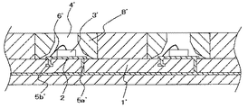
なお、本発明は上述の実施の形態に限定されるものではなく、本発明の要旨を逸脱しない範囲内で種々の変更を施すことは何等差し支えない。例えば、図9にパッケージの断面図で示すように、搭載部2は、凹部4の底面の絶縁基体1上面の搭載領域として、凹部4の底面に樹脂接着剤等の接合材を介して発光素子3を直接搭載するものとし、搭載部2の周囲に発光素子3の電極が接続される配線導体5a,5bを形成していても良い。この場合、搭載部2に発光素子3が搭載されるとともに、配線導体5a,5bに発光素子3の電極がボンディングワイヤ6a,6bを介して電気的に接続される。また、枠体8と枠体8の内周面に形成される金属層8bとの間にニッケル等から成る金属層を介在させていても良い。また、複数の発光素子3が搭載されたり、配線導体が形成されるものであっても良く、凹部4の中央部以外に発光素子3が搭載されていても構わない。
It should be noted that the present invention is not limited to the above-described embodiment, and various modifications can be made without departing from the scope of the present invention. For example, as shown in the cross-sectional view of the package in FIG. 9, the mounting
1:絶縁基体
2:搭載部
3:発光素子
4:凹部
5a,5b:配線導体
8:枠体
8b:金属層
1: Insulating substrate 2: Mounting portion 3: Light emitting element 4:
Claims (6)
Priority Applications (1)
| Application Number | Priority Date | Filing Date | Title |
|---|---|---|---|
| JP2004048560A JP2005243738A (en) | 2004-02-24 | 2004-02-24 | Accommodating light-emitting device and package therefor |
Applications Claiming Priority (1)
| Application Number | Priority Date | Filing Date | Title |
|---|---|---|---|
| JP2004048560A JP2005243738A (en) | 2004-02-24 | 2004-02-24 | Accommodating light-emitting device and package therefor |
Publications (1)
| Publication Number | Publication Date |
|---|---|
| JP2005243738A true JP2005243738A (en) | 2005-09-08 |
Family
ID=35025179
Family Applications (1)
| Application Number | Title | Priority Date | Filing Date |
|---|---|---|---|
| JP2004048560A Pending JP2005243738A (en) | 2004-02-24 | 2004-02-24 | Accommodating light-emitting device and package therefor |
Country Status (1)
| Country | Link |
|---|---|
| JP (1) | JP2005243738A (en) |
Cited By (9)
| Publication number | Priority date | Publication date | Assignee | Title |
|---|---|---|---|---|
| JP2007189501A (en) * | 2006-01-13 | 2007-07-26 | Matsushita Electric Ind Co Ltd | Electronic component |
| JP2008041811A (en) * | 2006-08-03 | 2008-02-21 | Ngk Spark Plug Co Ltd | Wiring circuit board, multiple-chip wiring circuit board, and method for manufacturing the wiring board |
| JP2011060961A (en) * | 2009-09-09 | 2011-03-24 | Toshiba Lighting & Technology Corp | Light-emitting device |
| JP2015043403A (en) * | 2013-07-26 | 2015-03-05 | 京セラ株式会社 | Package for storing light emitting element, light emitting device including the same, and light emitting display device including the light emitting device |
| JP2015062226A (en) * | 2013-09-23 | 2015-04-02 | 弘凱光電(深セン)有限公司 | Light emitting diode package structure for preventing lateral light leakage and method of manufacturing the same |
| US20180058642A1 (en) * | 2016-08-30 | 2018-03-01 | Nichia Corporation | Light emitting device |
| JP2018037500A (en) * | 2016-08-31 | 2018-03-08 | 日亜化学工業株式会社 | Light emitting element manufacturing method |
| JPWO2018043557A1 (en) * | 2016-08-31 | 2019-03-14 | Hoya株式会社 | Endoscope light source device, endoscope, and endoscope system |
| JP2021503184A (en) * | 2018-08-24 | 2021-02-04 | ケーティー・アンド・ジー・コーポレーション | Light emitting element and aerosol generator including it |
-
2004
- 2004-02-24 JP JP2004048560A patent/JP2005243738A/en active Pending
Cited By (13)
| Publication number | Priority date | Publication date | Assignee | Title |
|---|---|---|---|---|
| JP2007189501A (en) * | 2006-01-13 | 2007-07-26 | Matsushita Electric Ind Co Ltd | Electronic component |
| JP2008041811A (en) * | 2006-08-03 | 2008-02-21 | Ngk Spark Plug Co Ltd | Wiring circuit board, multiple-chip wiring circuit board, and method for manufacturing the wiring board |
| JP2011060961A (en) * | 2009-09-09 | 2011-03-24 | Toshiba Lighting & Technology Corp | Light-emitting device |
| JP2015043403A (en) * | 2013-07-26 | 2015-03-05 | 京セラ株式会社 | Package for storing light emitting element, light emitting device including the same, and light emitting display device including the light emitting device |
| JP2015062226A (en) * | 2013-09-23 | 2015-04-02 | 弘凱光電(深セン)有限公司 | Light emitting diode package structure for preventing lateral light leakage and method of manufacturing the same |
| US9236541B2 (en) | 2013-09-23 | 2016-01-12 | Brightek Optoelectronic (Shenzhen) Co., Ltd. | LED package structures for preventing lateral light leakage and method of manufacturing the same |
| US20180058642A1 (en) * | 2016-08-30 | 2018-03-01 | Nichia Corporation | Light emitting device |
| US10514135B2 (en) | 2016-08-30 | 2019-12-24 | Nichia Corporation | Light emitting device |
| JP2018037500A (en) * | 2016-08-31 | 2018-03-08 | 日亜化学工業株式会社 | Light emitting element manufacturing method |
| JPWO2018043557A1 (en) * | 2016-08-31 | 2019-03-14 | Hoya株式会社 | Endoscope light source device, endoscope, and endoscope system |
| JP2021503184A (en) * | 2018-08-24 | 2021-02-04 | ケーティー・アンド・ジー・コーポレーション | Light emitting element and aerosol generator including it |
| US11304449B2 (en) | 2018-08-24 | 2022-04-19 | Kt&G Corporation | Light-emitting element and aerosol generation device comprising same |
| JP7226904B2 (en) | 2018-08-24 | 2023-02-21 | ケーティー アンド ジー コーポレイション | Light-emitting device and aerosol generator including the same |
Similar Documents
| Publication | Publication Date | Title |
|---|---|---|
| JP2004327503A (en) | Package for light emitting element and light emitting device | |
| JP4072084B2 (en) | Light emitting element storage package and light emitting device | |
| JP2007096285A (en) | Light emitting device mounting substrate, light emitting device accommodating package, light emitting device and lighting device | |
| JP2005191111A (en) | Package for storing light emitting element, and light emitting device | |
| JP2004319939A (en) | Package for housing light emitting element and light emitting device | |
| JP4822980B2 (en) | Electronic component mounting substrate, electronic device, and method of manufacturing electronic device | |
| JP4132038B2 (en) | Light emitting device | |
| JP2005039194A (en) | Package for housing light emitting element, light emitting device, and luminair | |
| JP4295519B2 (en) | Light emitting element storage package and light emitting device | |
| JP2004228413A (en) | Package for housing light emitting element and light emitting device | |
| JP2007266222A (en) | Substrate for loading light emitting element, package for storing light emitting element, light emitting device and light system | |
| JP4659515B2 (en) | Light-emitting element mounting substrate, light-emitting element storage package, light-emitting device, and lighting device | |
| JP2005243738A (en) | Accommodating light-emitting device and package therefor | |
| JP4164006B2 (en) | Light emitting element storage package and light emitting device | |
| JP4484554B2 (en) | Lighting device | |
| JP2004259893A (en) | Package for housing light-emitting element and light-emitting device | |
| JP4336136B2 (en) | Light emitting element storage package and light emitting device | |
| JP2005216962A (en) | Package for containing light emitting element and light emitting device | |
| JP2009135536A (en) | Package for housing light emitting element and light emitting device | |
| JP2007208292A (en) | Light-emitting device | |
| JP4132039B2 (en) | Light emitting element storage package and light emitting device | |
| JP4336153B2 (en) | Light emitting element storage package and light emitting device | |
| JP2004172577A (en) | Package for housing light-emitting element and light-emitting device | |
| JP2007073718A (en) | Package for housing light emitting element | |
| JP4183175B2 (en) | Light emitting element storage package and light emitting device |