JP2005136437A - 半導体製造システム及びクリーンルーム - Google Patents
半導体製造システム及びクリーンルーム Download PDFInfo
- Publication number
- JP2005136437A JP2005136437A JP2005000288A JP2005000288A JP2005136437A JP 2005136437 A JP2005136437 A JP 2005136437A JP 2005000288 A JP2005000288 A JP 2005000288A JP 2005000288 A JP2005000288 A JP 2005000288A JP 2005136437 A JP2005136437 A JP 2005136437A
- Authority
- JP
- Japan
- Prior art keywords
- cleaning
- manufacturing system
- semiconductor manufacturing
- semiconductor
- container
- Prior art date
- Legal status (The legal status is an assumption and is not a legal conclusion. Google has not performed a legal analysis and makes no representation as to the accuracy of the status listed.)
- Pending
Links
- 239000004065 semiconductor Substances 0.000 title claims abstract description 81
- 238000004519 manufacturing process Methods 0.000 title claims abstract description 54
- 238000004140 cleaning Methods 0.000 claims abstract description 130
- 239000000758 substrate Substances 0.000 claims abstract description 54
- 238000000034 method Methods 0.000 claims abstract description 53
- 238000012545 processing Methods 0.000 claims abstract description 20
- XLYOFNOQVPJJNP-UHFFFAOYSA-N water Substances O XLYOFNOQVPJJNP-UHFFFAOYSA-N 0.000 claims abstract description 10
- 239000007788 liquid Substances 0.000 claims description 22
- 229910052751 metal Inorganic materials 0.000 claims description 20
- 239000002184 metal Substances 0.000 claims description 20
- 230000003647 oxidation Effects 0.000 claims description 17
- 238000007254 oxidation reaction Methods 0.000 claims description 17
- 238000000206 photolithography Methods 0.000 claims description 15
- CBENFWSGALASAD-UHFFFAOYSA-N Ozone Chemical compound [O-][O+]=O CBENFWSGALASAD-UHFFFAOYSA-N 0.000 claims description 13
- 229910052739 hydrogen Inorganic materials 0.000 claims description 13
- 239000004094 surface-active agent Substances 0.000 claims description 10
- DBJLJFTWODWSOF-UHFFFAOYSA-L nickel(ii) fluoride Chemical compound F[Ni]F DBJLJFTWODWSOF-UHFFFAOYSA-L 0.000 claims description 9
- 239000012298 atmosphere Substances 0.000 claims description 8
- NBVXSUQYWXRMNV-UHFFFAOYSA-N fluoromethane Chemical compound FC NBVXSUQYWXRMNV-UHFFFAOYSA-N 0.000 claims description 8
- 238000009792 diffusion process Methods 0.000 claims description 7
- 239000001257 hydrogen Substances 0.000 claims description 7
- 239000012535 impurity Substances 0.000 claims description 7
- 238000004544 sputter deposition Methods 0.000 claims description 6
- 238000012546 transfer Methods 0.000 claims description 5
- OKTJSMMVPCPJKN-UHFFFAOYSA-N Carbon Chemical compound [C] OKTJSMMVPCPJKN-UHFFFAOYSA-N 0.000 claims description 3
- 229910052799 carbon Inorganic materials 0.000 claims description 3
- 238000005268 plasma chemical vapour deposition Methods 0.000 claims description 3
- 238000003860 storage Methods 0.000 claims description 2
- 125000004435 hydrogen atom Chemical class [H]* 0.000 claims 1
- 239000000126 substance Substances 0.000 abstract description 42
- 238000013461 design Methods 0.000 abstract description 3
- 239000010408 film Substances 0.000 description 36
- 229910021642 ultra pure water Inorganic materials 0.000 description 33
- 239000012498 ultrapure water Substances 0.000 description 33
- 239000000243 solution Substances 0.000 description 14
- 230000032258 transport Effects 0.000 description 14
- 239000010410 layer Substances 0.000 description 13
- KRHYYFGTRYWZRS-UHFFFAOYSA-N Fluorane Chemical compound F KRHYYFGTRYWZRS-UHFFFAOYSA-N 0.000 description 10
- QGZKDVFQNNGYKY-UHFFFAOYSA-N Ammonia Chemical compound N QGZKDVFQNNGYKY-UHFFFAOYSA-N 0.000 description 8
- 239000007789 gas Substances 0.000 description 8
- 235000012431 wafers Nutrition 0.000 description 8
- 230000015572 biosynthetic process Effects 0.000 description 7
- 238000011109 contamination Methods 0.000 description 7
- 239000000203 mixture Substances 0.000 description 7
- 238000001020 plasma etching Methods 0.000 description 7
- 238000005468 ion implantation Methods 0.000 description 6
- IJGRMHOSHXDMSA-UHFFFAOYSA-N Atomic nitrogen Chemical compound N#N IJGRMHOSHXDMSA-UHFFFAOYSA-N 0.000 description 5
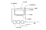
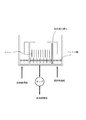
- 238000010586 diagram Methods 0.000 description 5
- 238000009434 installation Methods 0.000 description 5
- 229910052757 nitrogen Inorganic materials 0.000 description 5
- 239000012299 nitrogen atmosphere Substances 0.000 description 5
- UFHFLCQGNIYNRP-UHFFFAOYSA-N Hydrogen Chemical compound [H][H] UFHFLCQGNIYNRP-UHFFFAOYSA-N 0.000 description 4
- 229910021529 ammonia Inorganic materials 0.000 description 4
- 238000011161 development Methods 0.000 description 4
- 150000004767 nitrides Chemical class 0.000 description 4
- 238000005406 washing Methods 0.000 description 4
- 229910000838 Al alloy Inorganic materials 0.000 description 3
- VEXZGXHMUGYJMC-UHFFFAOYSA-N Hydrochloric acid Chemical compound Cl VEXZGXHMUGYJMC-UHFFFAOYSA-N 0.000 description 3
- 229910004298 SiO 2 Inorganic materials 0.000 description 3
- XUIMIQQOPSSXEZ-UHFFFAOYSA-N Silicon Chemical compound [Si] XUIMIQQOPSSXEZ-UHFFFAOYSA-N 0.000 description 3
- 238000004378 air conditioning Methods 0.000 description 3
- 238000005260 corrosion Methods 0.000 description 3
- 230000007797 corrosion Effects 0.000 description 3
- 239000000428 dust Substances 0.000 description 3
- 238000001704 evaporation Methods 0.000 description 3
- 230000008020 evaporation Effects 0.000 description 3
- 230000005284 excitation Effects 0.000 description 3
- 238000010438 heat treatment Methods 0.000 description 3
- 150000002739 metals Chemical class 0.000 description 3
- PXHVJJICTQNCMI-UHFFFAOYSA-N nickel Substances [Ni] PXHVJJICTQNCMI-UHFFFAOYSA-N 0.000 description 3
- 239000002245 particle Substances 0.000 description 3
- 229910021420 polycrystalline silicon Inorganic materials 0.000 description 3
- 229920005591 polysilicon Polymers 0.000 description 3
- 229910052710 silicon Inorganic materials 0.000 description 3
- 239000010703 silicon Substances 0.000 description 3
- 230000003746 surface roughness Effects 0.000 description 3
- 239000004215 Carbon black (E152) Substances 0.000 description 2
- YCKRFDGAMUMZLT-UHFFFAOYSA-N Fluorine atom Chemical compound [F] YCKRFDGAMUMZLT-UHFFFAOYSA-N 0.000 description 2
- MHAJPDPJQMAIIY-UHFFFAOYSA-N Hydrogen peroxide Chemical compound OO MHAJPDPJQMAIIY-UHFFFAOYSA-N 0.000 description 2
- QAOWNCQODCNURD-UHFFFAOYSA-N Sulfuric acid Chemical compound OS(O)(=O)=O QAOWNCQODCNURD-UHFFFAOYSA-N 0.000 description 2
- 229910052782 aluminium Inorganic materials 0.000 description 2
- 238000000137 annealing Methods 0.000 description 2
- 239000007864 aqueous solution Substances 0.000 description 2
- 230000003749 cleanliness Effects 0.000 description 2
- 238000000151 deposition Methods 0.000 description 2
- 230000008021 deposition Effects 0.000 description 2
- 230000009977 dual effect Effects 0.000 description 2
- 230000000694 effects Effects 0.000 description 2
- 238000005530 etching Methods 0.000 description 2
- 229910052731 fluorine Inorganic materials 0.000 description 2
- 239000011737 fluorine Substances 0.000 description 2
- 229930195733 hydrocarbon Natural products 0.000 description 2
- 150000002430 hydrocarbons Chemical class 0.000 description 2
- 150000002431 hydrogen Chemical class 0.000 description 2
- 230000010354 integration Effects 0.000 description 2
- 150000002500 ions Chemical class 0.000 description 2
- 238000002955 isolation Methods 0.000 description 2
- 239000000463 material Substances 0.000 description 2
- 229910052760 oxygen Inorganic materials 0.000 description 2
- 238000007747 plating Methods 0.000 description 2
- 238000009751 slip forming Methods 0.000 description 2
- 239000002351 wastewater Substances 0.000 description 2
- -1 RCA cleaning Chemical compound 0.000 description 1
- 239000004809 Teflon Substances 0.000 description 1
- 229920006362 Teflon® Polymers 0.000 description 1
- ATJFFYVFTNAWJD-UHFFFAOYSA-N Tin Chemical compound [Sn] ATJFFYVFTNAWJD-UHFFFAOYSA-N 0.000 description 1
- 239000002253 acid Substances 0.000 description 1
- 238000010306 acid treatment Methods 0.000 description 1
- 230000002411 adverse Effects 0.000 description 1
- 239000003513 alkali Substances 0.000 description 1
- 229910045601 alloy Inorganic materials 0.000 description 1
- 239000000956 alloy Substances 0.000 description 1
- XAGFODPZIPBFFR-UHFFFAOYSA-N aluminium Chemical compound [Al] XAGFODPZIPBFFR-UHFFFAOYSA-N 0.000 description 1
- 125000000129 anionic group Chemical group 0.000 description 1
- 125000004429 atom Chemical group 0.000 description 1
- 238000010923 batch production Methods 0.000 description 1
- 239000005380 borophosphosilicate glass Substances 0.000 description 1
- 125000002091 cationic group Chemical group 0.000 description 1
- 239000000470 constituent Substances 0.000 description 1
- 239000000356 contaminant Substances 0.000 description 1
- 230000007423 decrease Effects 0.000 description 1
- 230000003247 decreasing effect Effects 0.000 description 1
- 229910001873 dinitrogen Inorganic materials 0.000 description 1
- KPUWHANPEXNPJT-UHFFFAOYSA-N disiloxane Chemical class [SiH3]O[SiH3] KPUWHANPEXNPJT-UHFFFAOYSA-N 0.000 description 1
- 238000001035 drying Methods 0.000 description 1
- 238000011156 evaluation Methods 0.000 description 1
- 230000005484 gravity Effects 0.000 description 1
- 239000011261 inert gas Substances 0.000 description 1
- 239000011229 interlayer Substances 0.000 description 1
- 238000005339 levitation Methods 0.000 description 1
- 238000011068 loading method Methods 0.000 description 1
- 238000012423 maintenance Methods 0.000 description 1
- 239000012528 membrane Substances 0.000 description 1
- 229910052759 nickel Inorganic materials 0.000 description 1
- 230000003287 optical effect Effects 0.000 description 1
- 239000005416 organic matter Substances 0.000 description 1
- 230000001590 oxidative effect Effects 0.000 description 1
- 238000000059 patterning Methods 0.000 description 1
- OFNHPGDEEMZPFG-UHFFFAOYSA-N phosphanylidynenickel Chemical compound [P].[Ni] OFNHPGDEEMZPFG-UHFFFAOYSA-N 0.000 description 1
- 229920001343 polytetrafluoroethylene Polymers 0.000 description 1
- 239000004810 polytetrafluoroethylene Substances 0.000 description 1
- 230000001681 protective effect Effects 0.000 description 1
- 238000011084 recovery Methods 0.000 description 1
- 230000001846 repelling effect Effects 0.000 description 1
- 239000010935 stainless steel Substances 0.000 description 1
- 229910001220 stainless steel Inorganic materials 0.000 description 1
- 239000013589 supplement Substances 0.000 description 1
- 239000010409 thin film Substances 0.000 description 1
- 239000002699 waste material Substances 0.000 description 1
Images


Landscapes
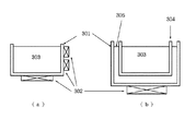
- Container, Conveyance, Adherence, Positioning, Of Wafer (AREA)
- Cleaning Or Drying Semiconductors (AREA)
Priority Applications (1)
| Application Number | Priority Date | Filing Date | Title |
|---|---|---|---|
| JP2005000288A JP2005136437A (ja) | 2005-01-04 | 2005-01-04 | 半導体製造システム及びクリーンルーム |
Applications Claiming Priority (1)
| Application Number | Priority Date | Filing Date | Title |
|---|---|---|---|
| JP2005000288A JP2005136437A (ja) | 2005-01-04 | 2005-01-04 | 半導体製造システム及びクリーンルーム |
Related Parent Applications (1)
| Application Number | Title | Priority Date | Filing Date |
|---|---|---|---|
| JP22079395A Division JP3923103B2 (ja) | 1995-08-29 | 1995-08-29 | 半導体製造システム及びクリーンルーム |
Publications (2)
| Publication Number | Publication Date |
|---|---|
| JP2005136437A true JP2005136437A (ja) | 2005-05-26 |
| JP2005136437A5 JP2005136437A5 (enExample) | 2007-01-18 |
Family
ID=34651090
Family Applications (1)
| Application Number | Title | Priority Date | Filing Date |
|---|---|---|---|
| JP2005000288A Pending JP2005136437A (ja) | 2005-01-04 | 2005-01-04 | 半導体製造システム及びクリーンルーム |
Country Status (1)
| Country | Link |
|---|---|
| JP (1) | JP2005136437A (enExample) |
Cited By (7)
| Publication number | Priority date | Publication date | Assignee | Title |
|---|---|---|---|---|
| WO2007034534A1 (ja) * | 2005-09-20 | 2007-03-29 | Tadahiro Ohmi | 半導体装置の製造方法及び半導体製造装置 |
| JP2007187436A (ja) * | 2005-12-13 | 2007-07-26 | Hokkaido Univ | クリーンユニット、連結クリーンユニット、クリーンユニットの運転方法およびクリーン作業室 |
| JP2009044042A (ja) * | 2007-08-10 | 2009-02-26 | Kurita Water Ind Ltd | 被処理物の浸漬型処理装置及び被処理物の処理方法 |
| JP2009131841A (ja) * | 2007-11-09 | 2009-06-18 | Kurabo Ind Ltd | 洗浄方法および洗浄装置 |
| JP2010153424A (ja) * | 2008-12-24 | 2010-07-08 | Tohoku Univ | 電子装置製造装置 |
| JP2011228406A (ja) * | 2010-04-16 | 2011-11-10 | Kurita Water Ind Ltd | オゾン水供給システム及びシリコンウエハの湿式酸化処理システム |
| JP2022185450A (ja) * | 2021-06-02 | 2022-12-14 | キヤノン株式会社 | 処理装置および物品製造方法 |
-
2005
- 2005-01-04 JP JP2005000288A patent/JP2005136437A/ja active Pending
Cited By (8)
| Publication number | Priority date | Publication date | Assignee | Title |
|---|---|---|---|---|
| WO2007034534A1 (ja) * | 2005-09-20 | 2007-03-29 | Tadahiro Ohmi | 半導体装置の製造方法及び半導体製造装置 |
| US8030182B2 (en) | 2005-09-20 | 2011-10-04 | Tadahiro Ohmi | Semiconductor device manufacturing method and semiconductor manufacturing apparatus |
| JP2007187436A (ja) * | 2005-12-13 | 2007-07-26 | Hokkaido Univ | クリーンユニット、連結クリーンユニット、クリーンユニットの運転方法およびクリーン作業室 |
| JP2009044042A (ja) * | 2007-08-10 | 2009-02-26 | Kurita Water Ind Ltd | 被処理物の浸漬型処理装置及び被処理物の処理方法 |
| JP2009131841A (ja) * | 2007-11-09 | 2009-06-18 | Kurabo Ind Ltd | 洗浄方法および洗浄装置 |
| JP2010153424A (ja) * | 2008-12-24 | 2010-07-08 | Tohoku Univ | 電子装置製造装置 |
| JP2011228406A (ja) * | 2010-04-16 | 2011-11-10 | Kurita Water Ind Ltd | オゾン水供給システム及びシリコンウエハの湿式酸化処理システム |
| JP2022185450A (ja) * | 2021-06-02 | 2022-12-14 | キヤノン株式会社 | 処理装置および物品製造方法 |
Similar Documents
| Publication | Publication Date | Title |
|---|---|---|
| CN112424916B (zh) | 半导体装置的制造方法、基板处理装置和记录介质 | |
| US6635565B2 (en) | Method of cleaning a dual damascene structure | |
| JP4891475B2 (ja) | エッチング処理した基板表面の洗浄方法 | |
| CN100377317C (zh) | 硅氧化膜的去除方法及处理装置 | |
| US7632756B2 (en) | Semiconductor processing using energized hydrogen gas and in combination with wet cleaning | |
| CN1954413A (zh) | 清洗衬底表面的方法 | |
| JP2009543344A (ja) | 液体メニスカスによるポストエッチウエハ表面洗浄 | |
| US6713401B2 (en) | Method for manufacturing semiconductor device | |
| JP3923103B2 (ja) | 半導体製造システム及びクリーンルーム | |
| JP2005136437A (ja) | 半導体製造システム及びクリーンルーム | |
| US6444582B1 (en) | Methods for removing silicon-oxy-nitride layer and wafer surface cleaning | |
| TWI398920B (zh) | Surface treatment of substrates | |
| US6955995B2 (en) | Methods of cleaning surfaces of copper-containing materials, and methods of forming openings to copper-containing substrates | |
| US6541391B2 (en) | Methods of cleaning surfaces of copper-containing materials, and methods of forming openings to copper-containing substrates | |
| JP2632261B2 (ja) | 基板表面の酸化膜の除去方法 | |
| US7141495B2 (en) | Methods and forming structures, structures and apparatuses for forming structures | |
| JP2001044429A (ja) | ゲート絶縁膜形成前処理方法及びその前処理装置 | |
| KR100247930B1 (ko) | 세정용액및이를이용한세정방법 | |
| US8932958B2 (en) | Device manufacturing and cleaning method | |
| Myeong et al. | Study on Ashing-less Dry Etching Process to Eliminate Q-time Defect Formation | |
| JP3201601B2 (ja) | 半導体基板の洗浄方法 | |
| US20050092348A1 (en) | Method for cleaning an integrated circuit device using an aqueous cleaning composition | |
| JPH07106298A (ja) | 半導体基板の処理方法 | |
| CN101157569A (zh) | 一种无损腐蚀碳化硅的方法 | |
| JPH11329982A (ja) | エピタキシャルウェーハの製造方法およびこれに用いる半導体製造装置 |
Legal Events
| Date | Code | Title | Description |
|---|---|---|---|
| A521 | Written amendment |
Effective date: 20061122 Free format text: JAPANESE INTERMEDIATE CODE: A523 |
|
| A977 | Report on retrieval |
Free format text: JAPANESE INTERMEDIATE CODE: A971007 Effective date: 20070308 |
|
| A131 | Notification of reasons for refusal |
Free format text: JAPANESE INTERMEDIATE CODE: A131 Effective date: 20070322 |
|
| A521 | Written amendment |
Effective date: 20070521 Free format text: JAPANESE INTERMEDIATE CODE: A523 |
|
| A02 | Decision of refusal |
Effective date: 20070718 Free format text: JAPANESE INTERMEDIATE CODE: A02 |