JP2005093591A - Solid electrolytic capacitor - Google Patents
Solid electrolytic capacitor Download PDFInfo
- Publication number
- JP2005093591A JP2005093591A JP2003322935A JP2003322935A JP2005093591A JP 2005093591 A JP2005093591 A JP 2005093591A JP 2003322935 A JP2003322935 A JP 2003322935A JP 2003322935 A JP2003322935 A JP 2003322935A JP 2005093591 A JP2005093591 A JP 2005093591A
- Authority
- JP
- Japan
- Prior art keywords
- anode
- anode lead
- lead frame
- lead member
- layer
- Prior art date
- Legal status (The legal status is an assumption and is not a legal conclusion. Google has not performed a legal analysis and makes no representation as to the accuracy of the status listed.)
- Pending
Links
Images


Classifications
-
- H—ELECTRICITY
- H01—ELECTRIC ELEMENTS
- H01G—CAPACITORS; CAPACITORS, RECTIFIERS, DETECTORS, SWITCHING DEVICES OR LIGHT-SENSITIVE DEVICES, OF THE ELECTROLYTIC TYPE
- H01G9/00—Electrolytic capacitors, rectifiers, detectors, switching devices, light-sensitive or temperature-sensitive devices; Processes of their manufacture
- H01G9/15—Solid electrolytic capacitors
-
- H—ELECTRICITY
- H01—ELECTRIC ELEMENTS
- H01G—CAPACITORS; CAPACITORS, RECTIFIERS, DETECTORS, SWITCHING DEVICES OR LIGHT-SENSITIVE DEVICES, OF THE ELECTROLYTIC TYPE
- H01G9/00—Electrolytic capacitors, rectifiers, detectors, switching devices, light-sensitive or temperature-sensitive devices; Processes of their manufacture
- H01G9/004—Details
- H01G9/008—Terminals
- H01G9/012—Terminals specially adapted for solid capacitors
-
- H—ELECTRICITY
- H01—ELECTRIC ELEMENTS
- H01G—CAPACITORS; CAPACITORS, RECTIFIERS, DETECTORS, SWITCHING DEVICES OR LIGHT-SENSITIVE DEVICES, OF THE ELECTROLYTIC TYPE
- H01G9/00—Electrolytic capacitors, rectifiers, detectors, switching devices, light-sensitive or temperature-sensitive devices; Processes of their manufacture
- H01G9/004—Details
- H01G9/04—Electrodes or formation of dielectric layers thereon
- H01G9/042—Electrodes or formation of dielectric layers thereon characterised by the material
Abstract
Description
本発明は、加工した陽極リードフレームを用いた固体電解コンデンサに関する。 The present invention relates to a solid electrolytic capacitor using a processed anode lead frame.
従来、固体電解コンデンサとして図5に示す構造のものが知られている。 Conventionally, a solid electrolytic capacitor having a structure shown in FIG. 5 is known.
この固体電解コンデンサは、弁作用金属(タンタル、ニオブ、チタン、アルミニウム等)の焼結体からなる陽極体1表面に、該陽極体表面を酸化させた誘電体皮膜層2、二酸化マンガン等の導電性無機材料、或いはTCNQ錯塩、導電性ポリマー等の導電性有機材料からなる固体電解質層3、カーボン、銀等からなる陰極引出層4を順次形成してコンデンサ素子15を構成し、前記陽極体1の一端面に植立された陽極リード部材16に陽極リードフレーム20を接続し、前記陰極引出層4に陰極リードフレーム21を導電性接着材5により接続し、前記コンデンサ素子15の外側にエポキシ樹脂等からなる外装樹脂層7にて被覆密封したものである。
This solid electrolytic capacitor has a surface of an
上記のような固体電解コンデンサに用いるリードフレーム基材としては、表面酸化が少ないこと、引張り強度が大きいこと、延性が充分で曲げ加工性に富むこと、高温特性たとえば 250℃以上の温度における機械的強度がすぐれていること、はんだとの濡れ性や耐候性が良好であること、エッチング性が良好であること、プレス打抜き性やプレス曲げ性のような加工性がすぐれること等の要件を具備することが要求されている。 Lead frame base materials used in the above solid electrolytic capacitors include low surface oxidation, high tensile strength, sufficient ductility and high bending workability, and high temperature characteristics such as mechanical properties at temperatures above 250 ° C. Requirements such as excellent strength, good wettability with solder and weather resistance, good etching properties, excellent workability such as press punchability and press bendability Is required to do.
これらの特性を比較的よく満足していることから、リードフレーム基材としては従来から42NiーFe合金が使用されてきたが、価格の点で未だ満足できるものではなく、また製造面でも直接はんだづけができないという問題があった。また、低ESR(直列等価抵抗)品が市場から求められてきているということもあり、近年、Cuの強度不足をFe,Ni,Sn,Cr,Zrなどで補ったCuを主成分とする合金が広く使用されるようになってきている。(例えば、特許文献1参照)
図4(a)は、従来の陽極リードフレーム20の陽極リード部材16との接続部22を示す部分下面図であり、同(b)図は線D−Dに沿って切断した部分断面図である。従来の陽極リードフレーム20は板状のものを用い、陽極リードフレーム20の陽極リード部材16との接続部22は、図4に示すように平面のものが用いられている。前記陽極リードフレーム20と前記陽極リード部材16は抵抗溶接により接続している。
FIG. 4A is a partial bottom view showing a
しかしながら、近年、広く使用されるようになってきたCu又はCuを主成分とする合金等の高導電率を有する金属材料は、その高導電性及び高熱伝導性により抵抗溶接の溶接強度が安定しない。そのため、その後の工程で陽極リード部材16と陽極リードフレーム20との溶接がはずれて歩留りが低下するという問題がある。
However, in recent years, metal materials having high electrical conductivity such as Cu or Cu-based alloys, which have been widely used in recent years, do not stabilize the welding strength of resistance welding due to their high electrical conductivity and high thermal conductivity. . For this reason, there is a problem in that the yield between the anode lead member 16 and the
本発明は、上記問題を鑑み、陽極リードフレーム20の陽極リード部材16との接続部22の形状を改良することにより、前記陽極リード部材16と前記陽極リードフレーム20との溶接強度を向上させ、溶接不良による歩留りを改善した固体電解コンデンサを提供することを目的とするものである。
In view of the above problems, the present invention improves the welding strength between the anode lead member 16 and the
本発明は、弁作用金属の焼結体からなる陽極体1に誘電体皮膜層2、固体電解質層3、陰極引出層4を順次形成し、前記陽極体1の一端面に陽極リード部材16が植立され、前記陽極リード部材16が陽極リードフレーム20に接続される固体電解コンデンサにおいて、前記陽極リードフレーム20の前記陽極リード部材16との接続部22に、凹凸部、梨地加工部、ディンプル加工部を設けることを特徴とする。
In the present invention, a
上記形状の陽極リードフレームを用いることにより、リードフレーム基材としてCu又はCuを主成分とする合金等の導電性・熱伝導性の高い材料を用いても、抵抗溶接の初期段階における溶接がスムーズに行われるため、抵抗溶接の強度が向上、安定する。よって、溶接不良を防ぎ歩留りを改善することができる。 By using the anode lead frame of the above shape, welding at the initial stage of resistance welding is smooth even when a highly conductive material such as Cu or an alloy containing Cu as a main component is used as the lead frame base material. Therefore, the strength of resistance welding is improved and stabilized. Therefore, poor welding can be prevented and yield can be improved.
本発明の実施例における固体電解コンデンサを図5に示す。 The solid electrolytic capacitor in the Example of this invention is shown in FIG.
この固体電解コンデンサは、タンタル焼結体からなる陽極体1表面に、該陽極体表面を酸化させた誘電体皮膜層2、導電性ポリマーからなる固体電解質層3、カーボン、銀等からなる陰極引出層4を順次形成してコンデンサ素子15を構成し、前記陽極体1の一端面に植立された陽極リード部材16に陽極リードフレーム20を抵抗溶接により接続し、前記陰極引出層4に陰極リードフレーム21を導電性接着材5により接続し、前記コンデンサ素子15の外側にエポキシ樹脂等からなる外装樹脂層7にて被覆密封したものである。
This solid electrolytic capacitor has a surface of an
ここでリードフレームフレーム基材としてCu又はCuを主成分とする合金を用いる。陽極リード部材16に接続する陽極リードフレーム20について、以下の実施例を示して説明する。
Here, Cu or an alloy containing Cu as a main component is used as the lead frame frame base material. The
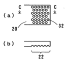
図1(a)は、陽極リードフレーム20の陽極リード部材16との接続部22を示す部分下面図であり、同(b)図は線A−Aに沿って切断した部分断面図である。前記陽極リードフレーム20の長手方向に略垂直に溝30を設けている。図(b)に示すように、溝の縁部には例えばプレス加工等による盛り上がり部があるが、例えばエッチング加工等により前記盛り上がり部が無いものでも同様の効果を有する。
FIG. 1A is a partial bottom view showing the
図2(a)は、陽極リードフレーム20の陽極リード部材16との接続部22を示す部分下面図であり、同(b)図は線B−Bに沿って切断した部分断面図である。前記接続部22表面に梨地加工部31を設けている。
2A is a partial bottom view showing the
図3(a)は、陽極リードフレーム20の陽極リード部材16との接続部22を示す部分下面図であり、同(b)図は線C−Cに沿って切断した部分断面図である。前記接続部22表面にディンプル加工部32を設けている。
FIG. 3A is a partial bottom view showing the
上記形状の陽極リードフレームを用いることにより、抵抗溶接の初期段階における溶接がスムーズに行われるため、抵抗溶接の強度が向上、安定する。よって、溶接不良を防ぎ歩留りを改善することができる。 By using the anode lead frame having the above-described shape, welding at the initial stage of resistance welding is smoothly performed, so that the strength of resistance welding is improved and stabilized. Therefore, poor welding can be prevented and yield can be improved.
実施例では、陽極リードフレーム基材としてCu又はCuを主成分とする合金を用いたが、導電性・熱伝導性の高い材料であればこれに限らず、同様に陽極リード部材と陽極リードフレームとの抵抗溶接不良を防止することができる。陽極リードフレームの溝形状として、実施例では図1のような形状を用いたが、溝30の形状・個数・配置は限定されない。陽極リードフレーム20の陽極リード部材16との接続部22に凹凸が形成されていれば同様の効果が得られる。
In the examples, Cu or an alloy containing Cu as a main component was used as the anode lead frame base material. However, the anode lead member and the anode lead frame are not limited to this as long as the material has high conductivity and thermal conductivity. It is possible to prevent poor resistance welding. As the groove shape of the anode lead frame, the shape as shown in FIG. 1 is used in the embodiment, but the shape, number, and arrangement of the
1 陽極体
2 誘電体皮膜層
3 固体電解質層
4 陰極引出層
5 導電性接着材
7 外装樹脂層
15 コンデンサ素子
16 陽極リード部材
20 陽極リードフレーム
21 陰極リードフレーム
22 陽極リードフレームの陽極リード部材との接続部
30 溝
31 梨地加工部
32 ディンプル加工部
DESCRIPTION OF
Claims (3)
A dielectric film layer, a solid electrolyte layer, and a cathode lead layer are sequentially formed on an anode body made of a sintered body of valve action metal, and an anode lead member is planted on one end surface of the anode body, and the anode lead member is an anode. A solid electrolytic capacitor connected to a lead frame, wherein a dimple processing portion is provided at a connection portion between the anode lead frame and the anode lead member.
Priority Applications (3)
| Application Number | Priority Date | Filing Date | Title |
|---|---|---|---|
| JP2003322935A JP2005093591A (en) | 2003-09-16 | 2003-09-16 | Solid electrolytic capacitor |
| US10/711,363 US7072172B2 (en) | 2003-09-16 | 2004-09-14 | Solid electrolytic capacitor |
| CNA2004100786792A CN1598984A (en) | 2003-09-16 | 2004-09-16 | Solid electrolytic capacitor |
Applications Claiming Priority (1)
| Application Number | Priority Date | Filing Date | Title |
|---|---|---|---|
| JP2003322935A JP2005093591A (en) | 2003-09-16 | 2003-09-16 | Solid electrolytic capacitor |
Publications (2)
| Publication Number | Publication Date |
|---|---|
| JP2005093591A true JP2005093591A (en) | 2005-04-07 |
| JP2005093591A5 JP2005093591A5 (en) | 2006-06-01 |
Family
ID=34270010
Family Applications (1)
| Application Number | Title | Priority Date | Filing Date |
|---|---|---|---|
| JP2003322935A Pending JP2005093591A (en) | 2003-09-16 | 2003-09-16 | Solid electrolytic capacitor |
Country Status (3)
| Country | Link |
|---|---|
| US (1) | US7072172B2 (en) |
| JP (1) | JP2005093591A (en) |
| CN (1) | CN1598984A (en) |
Families Citing this family (6)
| Publication number | Priority date | Publication date | Assignee | Title |
|---|---|---|---|---|
| CN102130300B (en) * | 2010-09-16 | 2012-07-04 | 昆山维信诺显示技术有限公司 | Organic electroluminescent device (OELD), display and application thereof |
| CN102005299A (en) * | 2010-11-23 | 2011-04-06 | 尼吉康株式会社 | Lead frame and manufacturing device therefore as well as solid electrolytic capacitor and manufacturing method thereof |
| JP2015230976A (en) * | 2014-06-05 | 2015-12-21 | 株式会社村田製作所 | Method for manufacturing solid electrolytic capacitor, and solid electrolytic capacitor |
| CN105047413A (en) * | 2015-08-11 | 2015-11-11 | 湖南艾华集团股份有限公司 | Chip aluminum electrolytic capacitor and production method |
| CN105810440A (en) * | 2015-10-27 | 2016-07-27 | 钰邦电子(无锡)有限公司 | Stack type solid electrolytic capacitor packaging structure and manufacturing method thereof |
| WO2020236566A1 (en) * | 2019-05-17 | 2020-11-26 | Avx Corporation | Delamination-resistant solid electrolytic capacitor |
Family Cites Families (6)
| Publication number | Priority date | Publication date | Assignee | Title |
|---|---|---|---|---|
| JPS63293147A (en) | 1987-05-26 | 1988-11-30 | Nippon Steel Corp | Production of iron-copper-chromium alloy strip for high-strength lead frame |
| JP3266205B2 (en) * | 1992-02-28 | 2002-03-18 | 日立エーアイシー株式会社 | Method for manufacturing solid electrolytic capacitor |
| JP3157748B2 (en) * | 1997-07-30 | 2001-04-16 | 富山日本電気株式会社 | Solid electrolytic capacitor using conductive polymer and method for manufacturing the same |
| JP3535014B2 (en) | 1998-06-19 | 2004-06-07 | 松下電器産業株式会社 | Electrode for electrolytic capacitor |
| JP4160223B2 (en) * | 1999-12-14 | 2008-10-01 | ローム株式会社 | Solid electrolytic capacitor |
| KR100466071B1 (en) * | 2002-05-22 | 2005-01-13 | 삼성전기주식회사 | A solid electrolytic condenser |
-
2003
- 2003-09-16 JP JP2003322935A patent/JP2005093591A/en active Pending
-
2004
- 2004-09-14 US US10/711,363 patent/US7072172B2/en active Active
- 2004-09-16 CN CNA2004100786792A patent/CN1598984A/en active Pending
Also Published As
| Publication number | Publication date |
|---|---|
| US7072172B2 (en) | 2006-07-04 |
| CN1598984A (en) | 2005-03-23 |
| US20050057889A1 (en) | 2005-03-17 |
Similar Documents
| Publication | Publication Date | Title |
|---|---|---|
| JP2006237195A (en) | Solid-state electrolytic capacitor | |
| TWI258779B (en) | Solid electrolytic capacitor and method of manufacturing the same | |
| CN102103934A (en) | Solid electrolytic capacitor and method for producing solid electrolytic capacitor | |
| JP2008085344A (en) | Tantalum capacitor | |
| TWI248097B (en) | Solid electrolytic capacitor | |
| JP4588630B2 (en) | Manufacturing method of chip-shaped solid electrolytic capacitor | |
| JP2011035335A (en) | Solid-state electrolytic capacitor and method of manufacturing the same | |
| JP2005093591A (en) | Solid electrolytic capacitor | |
| JP4508913B2 (en) | Solid electrolytic capacitor and method for producing anode material for solid electrolytic capacitor | |
| JP4895035B2 (en) | Solid electrolytic capacitor | |
| JP4646707B2 (en) | Solid electrolytic capacitor | |
| US10655241B2 (en) | Electrode foil production method and capacitor production method | |
| JP2005101418A (en) | Chip type solid electrolytic capacitor and its manufacturing method, and lead frame used therefor | |
| JP2010123728A (en) | Solid electrolytic capacitor | |
| JP4880431B2 (en) | Chip-shaped solid electrolytic capacitor | |
| JP2007096021A (en) | Chip type solid electrolytic capacitor and lead frame therefor | |
| JP2007227845A (en) | Solid electrolytic capacitor | |
| JP2005033097A (en) | Solid-state electrolytic capacitor | |
| JP2004247665A (en) | Solid-state electrolytic capacitor | |
| JP2010067876A (en) | Chip type solid electrolytic capacitor | |
| JP2008109007A (en) | Method of manufacturing bottom-surface electrode type solid-state electrolytic capacitor, and lead frame used for the same | |
| JP2006024966A (en) | Solid electrolytic capacitor | |
| JP4574544B2 (en) | Solid electrolytic capacitor | |
| JP2005228801A (en) | Chip-type solid electrolytic capacitor and lead frame used therefor | |
| JP4122019B2 (en) | Solid electrolytic capacitor |
Legal Events
| Date | Code | Title | Description |
|---|---|---|---|
| RD01 | Notification of change of attorney |
Free format text: JAPANESE INTERMEDIATE CODE: A7421 Effective date: 20051227 |
|
| A521 | Written amendment |
Free format text: JAPANESE INTERMEDIATE CODE: A523 Effective date: 20060406 |
|
| A621 | Written request for application examination |
Free format text: JAPANESE INTERMEDIATE CODE: A621 Effective date: 20060412 |
|
| A977 | Report on retrieval |
Free format text: JAPANESE INTERMEDIATE CODE: A971007 Effective date: 20080814 |
|
| A131 | Notification of reasons for refusal |
Free format text: JAPANESE INTERMEDIATE CODE: A131 Effective date: 20080826 |
|
| A521 | Written amendment |
Free format text: JAPANESE INTERMEDIATE CODE: A523 Effective date: 20081023 |
|
| A02 | Decision of refusal |
Free format text: JAPANESE INTERMEDIATE CODE: A02 Effective date: 20090428 |