JP2004523128A - High-performance flip-chip package for heat removal with minimal thermal mismatch - Google Patents
High-performance flip-chip package for heat removal with minimal thermal mismatch Download PDFInfo
- Publication number
- JP2004523128A JP2004523128A JP2003504467A JP2003504467A JP2004523128A JP 2004523128 A JP2004523128 A JP 2004523128A JP 2003504467 A JP2003504467 A JP 2003504467A JP 2003504467 A JP2003504467 A JP 2003504467A JP 2004523128 A JP2004523128 A JP 2004523128A
- Authority
- JP
- Japan
- Prior art keywords
- integrated circuit
- circuit device
- substrate
- contacts
- central region
- Prior art date
- Legal status (The legal status is an assumption and is not a legal conclusion. Google has not performed a legal analysis and makes no representation as to the accuracy of the status listed.)
- Pending
Links
Images


Classifications
-
- H—ELECTRICITY
- H01—ELECTRIC ELEMENTS
- H01L—SEMICONDUCTOR DEVICES NOT COVERED BY CLASS H10
- H01L23/00—Details of semiconductor or other solid state devices
- H01L23/34—Arrangements for cooling, heating, ventilating or temperature compensation ; Temperature sensing arrangements
- H01L23/42—Fillings or auxiliary members in containers or encapsulations selected or arranged to facilitate heating or cooling
- H01L23/433—Auxiliary members in containers characterised by their shape, e.g. pistons
- H01L23/4334—Auxiliary members in encapsulations
-
- H—ELECTRICITY
- H01—ELECTRIC ELEMENTS
- H01L—SEMICONDUCTOR DEVICES NOT COVERED BY CLASS H10
- H01L23/00—Details of semiconductor or other solid state devices
- H01L23/02—Containers; Seals
- H01L23/04—Containers; Seals characterised by the shape of the container or parts, e.g. caps, walls
- H01L23/053—Containers; Seals characterised by the shape of the container or parts, e.g. caps, walls the container being a hollow construction and having an insulating or insulated base as a mounting for the semiconductor body
- H01L23/055—Containers; Seals characterised by the shape of the container or parts, e.g. caps, walls the container being a hollow construction and having an insulating or insulated base as a mounting for the semiconductor body the leads having a passage through the base
-
- H—ELECTRICITY
- H01—ELECTRIC ELEMENTS
- H01L—SEMICONDUCTOR DEVICES NOT COVERED BY CLASS H10
- H01L23/00—Details of semiconductor or other solid state devices
- H01L23/12—Mountings, e.g. non-detachable insulating substrates
- H01L23/13—Mountings, e.g. non-detachable insulating substrates characterised by the shape
-
- H—ELECTRICITY
- H01—ELECTRIC ELEMENTS
- H01L—SEMICONDUCTOR DEVICES NOT COVERED BY CLASS H10
- H01L23/00—Details of semiconductor or other solid state devices
- H01L23/16—Fillings or auxiliary members in containers or encapsulations, e.g. centering rings
- H01L23/18—Fillings characterised by the material, its physical or chemical properties, or its arrangement within the complete device
- H01L23/24—Fillings characterised by the material, its physical or chemical properties, or its arrangement within the complete device solid or gel at the normal operating temperature of the device
-
- H—ELECTRICITY
- H01—ELECTRIC ELEMENTS
- H01L—SEMICONDUCTOR DEVICES NOT COVERED BY CLASS H10
- H01L23/00—Details of semiconductor or other solid state devices
- H01L23/48—Arrangements for conducting electric current to or from the solid state body in operation, e.g. leads, terminal arrangements ; Selection of materials therefor
- H01L23/488—Arrangements for conducting electric current to or from the solid state body in operation, e.g. leads, terminal arrangements ; Selection of materials therefor consisting of soldered or bonded constructions
- H01L23/498—Leads, i.e. metallisations or lead-frames on insulating substrates, e.g. chip carriers
- H01L23/49822—Multilayer substrates
-
- H—ELECTRICITY
- H01—ELECTRIC ELEMENTS
- H01L—SEMICONDUCTOR DEVICES NOT COVERED BY CLASS H10
- H01L2224/00—Indexing scheme for arrangements for connecting or disconnecting semiconductor or solid-state bodies and methods related thereto as covered by H01L24/00
- H01L2224/01—Means for bonding being attached to, or being formed on, the surface to be connected, e.g. chip-to-package, die-attach, "first-level" interconnects; Manufacturing methods related thereto
- H01L2224/10—Bump connectors; Manufacturing methods related thereto
- H01L2224/15—Structure, shape, material or disposition of the bump connectors after the connecting process
- H01L2224/16—Structure, shape, material or disposition of the bump connectors after the connecting process of an individual bump connector
- H01L2224/161—Disposition
- H01L2224/16151—Disposition the bump connector connecting between a semiconductor or solid-state body and an item not being a semiconductor or solid-state body, e.g. chip-to-substrate, chip-to-passive
- H01L2224/16221—Disposition the bump connector connecting between a semiconductor or solid-state body and an item not being a semiconductor or solid-state body, e.g. chip-to-substrate, chip-to-passive the body and the item being stacked
- H01L2224/16225—Disposition the bump connector connecting between a semiconductor or solid-state body and an item not being a semiconductor or solid-state body, e.g. chip-to-substrate, chip-to-passive the body and the item being stacked the item being non-metallic, e.g. insulating substrate with or without metallisation
- H01L2224/16227—Disposition the bump connector connecting between a semiconductor or solid-state body and an item not being a semiconductor or solid-state body, e.g. chip-to-substrate, chip-to-passive the body and the item being stacked the item being non-metallic, e.g. insulating substrate with or without metallisation the bump connector connecting to a bond pad of the item
-
- H—ELECTRICITY
- H01—ELECTRIC ELEMENTS
- H01L—SEMICONDUCTOR DEVICES NOT COVERED BY CLASS H10
- H01L2224/00—Indexing scheme for arrangements for connecting or disconnecting semiconductor or solid-state bodies and methods related thereto as covered by H01L24/00
- H01L2224/01—Means for bonding being attached to, or being formed on, the surface to be connected, e.g. chip-to-package, die-attach, "first-level" interconnects; Manufacturing methods related thereto
- H01L2224/26—Layer connectors, e.g. plate connectors, solder or adhesive layers; Manufacturing methods related thereto
- H01L2224/31—Structure, shape, material or disposition of the layer connectors after the connecting process
- H01L2224/32—Structure, shape, material or disposition of the layer connectors after the connecting process of an individual layer connector
- H01L2224/321—Disposition
- H01L2224/32151—Disposition the layer connector connecting between a semiconductor or solid-state body and an item not being a semiconductor or solid-state body, e.g. chip-to-substrate, chip-to-passive
- H01L2224/32221—Disposition the layer connector connecting between a semiconductor or solid-state body and an item not being a semiconductor or solid-state body, e.g. chip-to-substrate, chip-to-passive the body and the item being stacked
- H01L2224/32225—Disposition the layer connector connecting between a semiconductor or solid-state body and an item not being a semiconductor or solid-state body, e.g. chip-to-substrate, chip-to-passive the body and the item being stacked the item being non-metallic, e.g. insulating substrate with or without metallisation
-
- H—ELECTRICITY
- H01—ELECTRIC ELEMENTS
- H01L—SEMICONDUCTOR DEVICES NOT COVERED BY CLASS H10
- H01L2224/00—Indexing scheme for arrangements for connecting or disconnecting semiconductor or solid-state bodies and methods related thereto as covered by H01L24/00
- H01L2224/73—Means for bonding being of different types provided for in two or more of groups H01L2224/10, H01L2224/18, H01L2224/26, H01L2224/34, H01L2224/42, H01L2224/50, H01L2224/63, H01L2224/71
- H01L2224/732—Location after the connecting process
- H01L2224/73201—Location after the connecting process on the same surface
- H01L2224/73203—Bump and layer connectors
- H01L2224/73204—Bump and layer connectors the bump connector being embedded into the layer connector
-
- H—ELECTRICITY
- H01—ELECTRIC ELEMENTS
- H01L—SEMICONDUCTOR DEVICES NOT COVERED BY CLASS H10
- H01L2224/00—Indexing scheme for arrangements for connecting or disconnecting semiconductor or solid-state bodies and methods related thereto as covered by H01L24/00
- H01L2224/73—Means for bonding being of different types provided for in two or more of groups H01L2224/10, H01L2224/18, H01L2224/26, H01L2224/34, H01L2224/42, H01L2224/50, H01L2224/63, H01L2224/71
- H01L2224/732—Location after the connecting process
- H01L2224/73251—Location after the connecting process on different surfaces
- H01L2224/73253—Bump and layer connectors
-
- H—ELECTRICITY
- H01—ELECTRIC ELEMENTS
- H01L—SEMICONDUCTOR DEVICES NOT COVERED BY CLASS H10
- H01L23/00—Details of semiconductor or other solid state devices
- H01L23/02—Containers; Seals
- H01L23/10—Containers; Seals characterised by the material or arrangement of seals between parts, e.g. between cap and base of the container or between leads and walls of the container
-
- H—ELECTRICITY
- H01—ELECTRIC ELEMENTS
- H01L—SEMICONDUCTOR DEVICES NOT COVERED BY CLASS H10
- H01L2924/00—Indexing scheme for arrangements or methods for connecting or disconnecting semiconductor or solid-state bodies as covered by H01L24/00
- H01L2924/0001—Technical content checked by a classifier
- H01L2924/00014—Technical content checked by a classifier the subject-matter covered by the group, the symbol of which is combined with the symbol of this group, being disclosed without further technical details
-
- H—ELECTRICITY
- H01—ELECTRIC ELEMENTS
- H01L—SEMICONDUCTOR DEVICES NOT COVERED BY CLASS H10
- H01L2924/00—Indexing scheme for arrangements or methods for connecting or disconnecting semiconductor or solid-state bodies as covered by H01L24/00
- H01L2924/01—Chemical elements
- H01L2924/01057—Lanthanum [La]
-
- H—ELECTRICITY
- H01—ELECTRIC ELEMENTS
- H01L—SEMICONDUCTOR DEVICES NOT COVERED BY CLASS H10
- H01L2924/00—Indexing scheme for arrangements or methods for connecting or disconnecting semiconductor or solid-state bodies as covered by H01L24/00
- H01L2924/01—Chemical elements
- H01L2924/01079—Gold [Au]
-
- H—ELECTRICITY
- H01—ELECTRIC ELEMENTS
- H01L—SEMICONDUCTOR DEVICES NOT COVERED BY CLASS H10
- H01L2924/00—Indexing scheme for arrangements or methods for connecting or disconnecting semiconductor or solid-state bodies as covered by H01L24/00
- H01L2924/095—Indexing scheme for arrangements or methods for connecting or disconnecting semiconductor or solid-state bodies as covered by H01L24/00 with a principal constituent of the material being a combination of two or more materials provided in the groups H01L2924/013 - H01L2924/0715
- H01L2924/097—Glass-ceramics, e.g. devitrified glass
- H01L2924/09701—Low temperature co-fired ceramic [LTCC]
-
- H—ELECTRICITY
- H01—ELECTRIC ELEMENTS
- H01L—SEMICONDUCTOR DEVICES NOT COVERED BY CLASS H10
- H01L2924/00—Indexing scheme for arrangements or methods for connecting or disconnecting semiconductor or solid-state bodies as covered by H01L24/00
- H01L2924/10—Details of semiconductor or other solid state devices to be connected
- H01L2924/102—Material of the semiconductor or solid state bodies
- H01L2924/1025—Semiconducting materials
- H01L2924/10251—Elemental semiconductors, i.e. Group IV
- H01L2924/10253—Silicon [Si]
-
- H—ELECTRICITY
- H01—ELECTRIC ELEMENTS
- H01L—SEMICONDUCTOR DEVICES NOT COVERED BY CLASS H10
- H01L2924/00—Indexing scheme for arrangements or methods for connecting or disconnecting semiconductor or solid-state bodies as covered by H01L24/00
- H01L2924/15—Details of package parts other than the semiconductor or other solid state devices to be connected
- H01L2924/151—Die mounting substrate
- H01L2924/1515—Shape
- H01L2924/15153—Shape the die mounting substrate comprising a recess for hosting the device
-
- H—ELECTRICITY
- H01—ELECTRIC ELEMENTS
- H01L—SEMICONDUCTOR DEVICES NOT COVERED BY CLASS H10
- H01L2924/00—Indexing scheme for arrangements or methods for connecting or disconnecting semiconductor or solid-state bodies as covered by H01L24/00
- H01L2924/15—Details of package parts other than the semiconductor or other solid state devices to be connected
- H01L2924/151—Die mounting substrate
- H01L2924/15165—Monolayer substrate
-
- H—ELECTRICITY
- H01—ELECTRIC ELEMENTS
- H01L—SEMICONDUCTOR DEVICES NOT COVERED BY CLASS H10
- H01L2924/00—Indexing scheme for arrangements or methods for connecting or disconnecting semiconductor or solid-state bodies as covered by H01L24/00
- H01L2924/15—Details of package parts other than the semiconductor or other solid state devices to be connected
- H01L2924/151—Die mounting substrate
- H01L2924/1517—Multilayer substrate
-
- H—ELECTRICITY
- H01—ELECTRIC ELEMENTS
- H01L—SEMICONDUCTOR DEVICES NOT COVERED BY CLASS H10
- H01L2924/00—Indexing scheme for arrangements or methods for connecting or disconnecting semiconductor or solid-state bodies as covered by H01L24/00
- H01L2924/15—Details of package parts other than the semiconductor or other solid state devices to be connected
- H01L2924/151—Die mounting substrate
- H01L2924/153—Connection portion
- H01L2924/1531—Connection portion the connection portion being formed only on the surface of the substrate opposite to the die mounting surface
- H01L2924/15311—Connection portion the connection portion being formed only on the surface of the substrate opposite to the die mounting surface being a ball array, e.g. BGA
-
- H—ELECTRICITY
- H01—ELECTRIC ELEMENTS
- H01L—SEMICONDUCTOR DEVICES NOT COVERED BY CLASS H10
- H01L2924/00—Indexing scheme for arrangements or methods for connecting or disconnecting semiconductor or solid-state bodies as covered by H01L24/00
- H01L2924/15—Details of package parts other than the semiconductor or other solid state devices to be connected
- H01L2924/151—Die mounting substrate
- H01L2924/156—Material
- H01L2924/15786—Material with a principal constituent of the material being a non metallic, non metalloid inorganic material
- H01L2924/15787—Ceramics, e.g. crystalline carbides, nitrides or oxides
-
- H—ELECTRICITY
- H01—ELECTRIC ELEMENTS
- H01L—SEMICONDUCTOR DEVICES NOT COVERED BY CLASS H10
- H01L2924/00—Indexing scheme for arrangements or methods for connecting or disconnecting semiconductor or solid-state bodies as covered by H01L24/00
- H01L2924/15—Details of package parts other than the semiconductor or other solid state devices to be connected
- H01L2924/161—Cap
- H01L2924/1615—Shape
- H01L2924/16152—Cap comprising a cavity for hosting the device, e.g. U-shaped cap
-
- H—ELECTRICITY
- H01—ELECTRIC ELEMENTS
- H01L—SEMICONDUCTOR DEVICES NOT COVERED BY CLASS H10
- H01L2924/00—Indexing scheme for arrangements or methods for connecting or disconnecting semiconductor or solid-state bodies as covered by H01L24/00
- H01L2924/15—Details of package parts other than the semiconductor or other solid state devices to be connected
- H01L2924/161—Cap
- H01L2924/1615—Shape
- H01L2924/16195—Flat cap [not enclosing an internal cavity]
-
- H—ELECTRICITY
- H01—ELECTRIC ELEMENTS
- H01L—SEMICONDUCTOR DEVICES NOT COVERED BY CLASS H10
- H01L2924/00—Indexing scheme for arrangements or methods for connecting or disconnecting semiconductor or solid-state bodies as covered by H01L24/00
- H01L2924/15—Details of package parts other than the semiconductor or other solid state devices to be connected
- H01L2924/181—Encapsulation
- H01L2924/1815—Shape
- H01L2924/1816—Exposing the passive side of the semiconductor or solid-state body
- H01L2924/18161—Exposing the passive side of the semiconductor or solid-state body of a flip chip
-
- H—ELECTRICITY
- H01—ELECTRIC ELEMENTS
- H01L—SEMICONDUCTOR DEVICES NOT COVERED BY CLASS H10
- H01L2924/00—Indexing scheme for arrangements or methods for connecting or disconnecting semiconductor or solid-state bodies as covered by H01L24/00
- H01L2924/30—Technical effects
- H01L2924/35—Mechanical effects
- H01L2924/351—Thermal stress
- H01L2924/3511—Warping
Abstract
この発明は、中にフリップチップダイを受取るために第1の主要な面上に中央キャビティ面積を含む、改善された半導体フリップチップパッケージを提供する。パッケージ基板は、実質的に、支持部および補強材としての役割を果たす単一の材料からできており、シリコンダイへのフリップチップ配線のためのすべての接続点をキャビティ床内に備える。一体化されたキャビティ壁は、パッケージの補強材としての役割を果たし、別個の補強材料を接着しなくても、構成全体の所要の機械的安定性をもたらす。キャビティ壁は、電気的性能を高めるバイパスコンデンサを作り出すよう追加の金属化の工程を含み得る。この発明は、シリコンダイを覆ってパッケージの熱的性能を高めるためのオプションの方法を開示する。The present invention provides an improved semiconductor flip chip package that includes a central cavity area on a first major surface for receiving a flip chip die therein. The package substrate is substantially made of a single material that acts as a support and stiffener, with all connection points in the cavity floor for flip chip wiring to the silicon die. The integrated cavity wall serves as a stiffener for the package and provides the required mechanical stability of the entire configuration without the need to bond separate stiffeners. The cavity walls may include additional metallization steps to create a bypass capacitor that enhances electrical performance. The present invention discloses an optional method for enhancing the thermal performance of the package over the silicon die.
Description
【技術分野】
【0001】
発明の分野
この発明は、集積回路のパッケージングに関し、特に、広範囲のダイの寸法に対する表面マウントアセンブリ温度のばらつきを最小限にするフリップチップ配線されたパッケージングに関する。
【背景技術】
【0002】
発明の背景
過去数年間に、ネットワーク化、記憶、およびハイエンドCPU計算等の高性能のアプリケーションを対象とした集積回路パッケージにおいてフリップチップ配線を用いることを目指す取組みが急増してきた。フリップチップ配線されたパッケージにおけるこの取組みについてはいくつかの理由がある。この高レベルの取組みを促進する主要な原動力の1つは、これらのよりI/O集約型の集積回路に対するパッドの制限に対処するフリップチップ配線の能力である。現在の集積回路のダイは、数百万のトランジスタを一緒に組込んで、1つのチップ上に複雑なシステムを形成することができる。これらの複雑なシステムでは、信号ならびに関連する接地および多電圧パッドを、チップから支持パッケージへ、次いで数百の外部接続へと接続することが必要とされる。これらの装置においては、従来の周辺のパッド構造の空間が足りなくなり、フリップチップ配線で用いられるパッドアレイ構造が実行可能な好ましいオプションとなる。
【0003】
フリップチップ配線がこれらの高性能の装置のために普及した別の理由は、短いI/O配線によってもたらされた付加的な電気的性能と、チップ上に必要とされる、正確な位置への電源および接地接続を支持するフリップチップ配線の能力とである。
【0004】
フリップチップ配線を実現するための、現在一般的に利用可能な高性能パッケージングソリューションのうちいくつかは、積層された薄膜を用いる、多層セラミック基板、ガラスセラミック基板、および積層型多層プリント配線板(PWB)を含む。表面マウントの応用例ではこれらのパッケージのほとんどが用いられる。フリップチップ配線を備えたパッケージは、表面マウントアセンブリ温度の衝撃に耐え得るものでなければならず、かつ、予期される使用条件に対して、フリップチップ接合部および外部のボール接合部に対する許容可能なボードレベルの信頼性を有する。
【0005】
パッケージ内に配置されるフリップチップダイは、裏返され、ダイの活性面のほとんどを覆うバンプアレイ形式で、チップの活性面上の導電ボールまたはバンプを介して、パッケージまたは基板上にパターニングされた導体に接続されなければならない。ダイと基板の間の接合部の耐用年数を延ばすために、典型的にはエポキシの欠肉材料が供給され、接合部のまわりで硬化してその界面をともに保持することを可能にする。この段階では、結果として生じるアセンブリは一般的にキャップレスと称され、このキャップレス形式で装置を展開させるエンドユーザもいる。エンドアプリケーションに応じて、ヒートシンク、ヒートスプレッダ、および封止材料の組合せを伴うさまざまな熱強化方法を適用してもよい。これらの方法のうちいくつかの熱的かつ機械的な影響は、含まれる材料および界面の数のせいで、取組むべき課題となる可能性がある。
【0006】
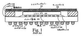
図1は、外部のプリント回路板に接続するための外部のはんだボール106を備えた典型的な基板105を用いる先行技術のフリップチップボールグリッドアレイパッケージの断面図を示す。リム(Lim)他による米国特許第6,020,221号には、この種類の構造が開示される。シリコンチップまたはダイ107は、ダイ107の活性面に形成されるはんだバンプ109によって基板105に接続されてから、シリコンウェハから分離される。組立中、これらバンプを備えたシリコンダイは、好ましくははんだリフローによって、パッケージ基板105の上方の面上のアレイ接点111にバンプ109が接するように設置されるが、但し、他の取付方法も可能である。ダイと基板との間の空間は、通常、欠肉材料110、たとえばエポキシでもって、毛管作用によって埋められる。次いで、材料110を適所で硬化させる。欠肉材料は、電気絶縁性であり、必要な場合、熱伝導性であってもよい。
【0007】
基板の平坦性および剛性を維持するために、補強材103が基板105の周囲に配置され、エポキシ104により適所に保持され得る。リム(Lim)他による米国特許第6,020,221号にもこの補強材特性が開示される。場合によっては、ダイの装着プロセスの前に補強材を取付けてもよい。ダイ107の熱的性能のために、典型的には金属でできたヒートスプレッダまたは被覆ヒートシンク101は、サーマルグリース108でもってダイ107に接続され、エポキシ102でもって補強材103に接続される。熱強化された構造は公知である。たとえば、キア(Chia)他による米国特許第5,568,683号は、熱強化されたパッケージを示す。図1には示されないが、はんだバンプ109をそれぞれの外部のはんだボール106に接続する電気的接続が基板105内に形成される。
【0008】
基板105のために有機積層材料を用いることができる。代替的には、米国特許第6,201,301号においてラン・ホアン(Lan Hoang)が指摘するように、窒化アルミニウム、炭化珪素、ガラスセラミック、およびポリイミドなどの他の材料を、基板105のために用いてもよい。これらのフリップチップパッケージ基板は、典型的には、絶縁層間に延在する導体で複数の層に形成される。基板の上面上の複数の電気伝導接触パッド111からのトレースは、このトレースが、ダイ107に接する面と反対側の外面における対応する外部のボールパッド113で終わるまで、次の層を接続する電気的バイアスを経由する。有機材料の場合、これらの層のいくつかは、いっしょに積層されるかまたは一連の積層技術を用いることにより、基板を形成する。セラミック基板の場合、金属回路を頂部に備えた薄いセラミック層を積み重ね、かつ高温で焼成して、所望の構造を得る。高性能のセラミックおよび積層ボールグリッドアレイパッケージ(BGA)を提供する製造業者には、富士通、京セラ、NTK、3M(ゴア(Gore))、ユニキャップ(Unicap)およびイビデン(Ibiden)が含まれる。
【0009】
図2には、図1に記載されるものと類似の材料特性を共有するベース基板105を備えた別の先行技術のパッケージが示される。検討しやすくするために、同じ構造および機能を有する要素には同じ参照番号が付される。図2に示される構造では、一体成形のヒートスプレッダカバー201がベース基板の補強機能を果たす。一体成形の蓋は、同時に補強および放熱の機能を果たす。
【0010】
これらの従来の高性能フリップチップパッケージング構造のうちのほとんどに関わる問題は、その構造が比較的複雑であり、製造が困難な可能性があるという点である。これらは、パッケージを形成するために接着されるいくつかの異なった種類の材料を含む。この構造が通常の製作プロセス温度にさらされると、これらの材料間の熱の相互作用により、歪み、平面性の欠如および接触の問題が生じるおそれがある。さらに、通常の構成要素のマウントリフロー温度およびその後の温度、ならびにこのように複雑な複合構造が使用中に経験する電源周期が、熱的かつ機械的な破損につながるおそれがある。
【0011】
パッケージングされた装置は、異なる熱膨張係数(CTE)を有するいくつかの材料をひとつにまとめる。中でもシリコンダイは、CTEが2.5〜3ppm/℃である。基板の種類は、CTEが約5.0ppm/℃であるセラミックから、CTEが典型的には8〜12ppm/℃であるガラスセラミック、さらには、CTEが16.0ppm/℃を超える有機積層と様々である。熱硬化性エポキシを基にした封止材料および欠肉は、CTEが、これらのガラス転移温度Tgよりも低い約12〜18ppm/℃であり、かつ、これらのTgよりはるかに高い50〜70ppm/℃などの数値であり得る。ヒートシンクおよびヒートスプレッダは、典型的には銅でできており、典型的なCTE値は16.5ppm/℃である。現代の電子パッケージングにおける課題のうち1つは、対象の温度を超える、密接に適合したCTEを伴う材料を選択することである。このように、構成要素の製造、試験、基板上へのリフロー中の温度のばらつきの通常の発生源と、その後の使用中における電源周期とにより、CTEの応力により誘起される破損が最小限となり、こうして信頼性が改善される。
【0012】
図1の構造は、全体的なパッケージ剛性を得るために窓型補強材103を用いる。これがない場合、硬化後に欠肉が冷えると基板105が曲がる可能性がある。CTE値が基板105および補強材103に適合するように材料を選択する努力がなされるが、温度の範囲に関して完全に適合させることが常に可能とは限らない。図2のカバー構造201は、類似の剛性機能を果たす。また、接着104におけるいかなる膨張差のばらつきまたは破損も、機能および信頼性の低下につながるおそれがある。ダイ107および基板105でできた複合構成要素の構造の曲げを最小限にすることが望ましい。
【発明の開示】
【発明が解決しようとする課題】
【0013】
発明の概要
この発明は、これらのパッケージをより簡単に組立て、組立中の歪みを減じ、高性能パッケージの基本となる機能を変えることなく界面応力を最小限にするために、これらパッケージを製造する際に用いられる構造を向上させることを目的としている。
【課題を解決するための手段】
【0014】
この発明は、熱強化されたフリップチップBGAパッケージ基板においてヒートシンクを実現するのに必要な材料の種類と界面との数を最小限にする、改善された半導体パッケージを提供する。この発明に従って、ダイのためのキャビティ面積を組込んだ単一の構造は、支持基板および補強材の両方としての役割を果たす。フリップチップ配線が装着されたダイが中にあるキャビティを備えた単一の硬質基板は、単純な製造工程で剛性機能に対処し、より重要なことには、パッケージの壁と床との間で完全に適合したCTEを提供するので、CTEによる界面の信頼性の問題を生ずることはない。CTEを、キャビティパッケージの壁および床と適合させることにより、キャビティ床の周辺と内側のキャビティ壁の端部との間にある面内のCTEとZ−軸のCTEとの差について懸念することなく、封止材料を用いることが可能となる。
【0015】
外部のボールとの接触点は、ダイの境界内のキャビティ面積における一連のパッドで終わる。この構造上の構成により、動作温度の範囲を超える異なったCTEを有する異質の材料から作られた接着された補強材に関連付けられる界面応力が実質的になくなる。単一体構造は、導電性の配線層を含み、ここでは、導体は、シリコンダイ上の導体を、パッケージの外部にあるはんだボール等の導体に接続するよう形成される。基部とともに用いることのできるいくつかのオプションの上面および封止材料を記載する。
【0016】
この単一体構造の形状により、これを、ダイを保護する封止材料を受取るための容器またはダムとして用いることが可能となる。さらに、床および壁の性質が同じなので、この構成は、適切なCTEを有する封止材料を選択するのに適している。
【0017】
同様に、この発明の特徴として、キャビティ壁は連続する基板の一部であるので、回路機能をいくらか壁に延在させることが可能である。特に、壁におけるプレートコンデンサは、ダイの近くで高周波数のバイパスコンデンサとしての役割を果たすことができる。単一体構造の壁は、高周波数のバイパスのために1つ以上のチップコンデンサを形成する、間に差込まれた導電性の層を含み得る。単一体構造が、主として、セラミックまたはガラス材料などの適度な誘電率(5〜9ppm/℃)を伴う材料から形成される場合、導電性および絶縁性の材料が、連続する薄い層に形成されて、誘電体としてセラミックを備えた平行なプレートコンデンサを作り出し得る。シリコンチップに隣接してコンデンサを配置することにより、シリコンチップが経験する電源および接地電圧に対し即座に電荷安定性がもたらされ、これにより、グラウンドバウンスが減じられ、集積回路装置の高速の切換特性が改善される。
【発明を実施するための最良の形態】
【0018】
詳細な説明
図3は、パッケージ305が周囲の壁305aによって囲まれる中央の凹型領域を備えた一体構造を含む、この発明の一実施例を示す。シリコンダイ107は中央の凹型領域内に位置決めされて、はんだバンプ109によって中央の凹型領域において複数の接点111に電気的に接続され、欠肉エポキシ110によって適所に保持される。図1および図2の先行技術の構造とは異なり、パッケージ305は単に平坦なだけではなく、下方の基板床領域305bを備えた単一の連続片として周囲の壁305aを組込む。この構造自体は、先行技術の構造で用いられるのと類似の材料特性を有し得る。パッケージ305のための材料積層は、CTEが12ppm/℃であるHiTCE集積回路基板として、京セラ(日本)から調達され得る。パッケージ305では、図示のとおり、キャビティ床の接続金属は、ダイ107上のバンプ109の類似の配置に対応する一連の接触パッド111を規定するようパターニングされる。接触パッド111は好ましくは銅であり、これがニッケルおよび次に金でめっきされてから、バンプ109が形成される。接触パッド111からのバイアスおよびトレースは、金属化層および絶縁材料を通って進み、外部のボールパッド113に達して外部のボール106に接触するようにする。
【0019】
床または下方の基板層305bを形成し、パッケージ305の壁305aを単一の片として堅くすることにより、接着される従来の金属補強材103に通常関連付けられる熱の不整合がなくなり、図1および図2の構造に生じるおそれのある層間剥離の可能性もなくなる。
【0020】
パッケージ305においてシリコンダイ107を実現するためのいくつかの構造が、より簡単な構造を利用して示される。
【0021】
図3では、好ましくは薄さに対応した金属でできたヒートスプレッダ101が、サーマルグリース108でシリコンダイ107に接続され、エポキシ102で不連続な部分に接着させることによりパッケージ305の壁305aの頂部に取付けられる(不連続なので、空気または溜まった水分をリフロー中に逃すことが可能となる)。これにより、完全なヒートシンクを備えた、熱強化されたパッケージが作り出される。
【0022】
図4では、シリコンダイ107は露出されたままであるが、熱伝導性の封止材料411によって保持および保護される。シリコンダイ107の裏面は、キャビティ壁305aの頂部と水平に位置決めされる。より低プロファイルの熱強化されたパッケージが結果として生じる。同様に、この実施例における封止材料は、一体型のキャビティ床およびダム壁と接触しており、異なった材料の膨張差とその付近で起こり得る層間剥離との可能性を最小限にする。
【0023】
図5には、このパッケージングを用いて別の実施例が示され、ここでは、熱放散は主要な目的ではないかもしれないが、シリコンダイを覆い、かつ低プロファイルのパッケージを作り出す必要性を最優先にすることができる。この実施例では、シリコンダイ507は装着の前に薄くされるので、封止材料は、ダイ全体および近接する面積を完全に覆うことができる。この構成の熱の必要性に合わせて封止材料を選択することができる。こうして、図5では、ダイ507がパッケージ305内の凹部に配置され、封止材料511がダイ507の側面および露出された面の両方を覆う。
【0024】
図6では、埋込型または組込式のヒートスプレッダ601は、ダイ507の露出された面を覆い、封止材料611と嵌合してダイ507を保護し、所望の場合、外部のヒートシンク(図示せず)のために取付けられる。
【0025】
パッケージ壁におけるチップコンデンサ
図7には、パッケージ壁305aおよび下方の基板面積305bの一部がより詳細に示され、パッケージ305内の電気的接続のいくつかが例示される。図7の実施例では、高くなった周囲の壁領域305aは、1つ以上のチップコンデンサを含む。各コンデンサは、各コンデンサプレート712および713が複数の層を有し、1つのプレートの層が他のプレートの層と交互し、絶縁によって隔てられるように形成される。図7では、コンデンサプレート712の層712a、712bおよび712cは、コンデンサプレート713の層713a、713bおよび713cと交互する。薄い絶縁層によってのみ隔てられるこれらの層を近接させて配置することにより、静電容量値を大きくすることができる。さらに、チップコンデンサ(またはコンデンサ)をパッケージ壁内に配置することにより、チップの近くにコンデンサが据えられるので、高速の切換えが存在する状態で安定した電源電圧を維持することができる。特に、コンデンサは、シリアル入出力バス上で発生する高速の入出力切換に対応することができる。
【0026】
図7はまた、下方の基板面積305b内の金属化層714を示す。はんだボール106はボールパッド113に結合され、これらボールパッド113は、バイアス716を介して、金属化層714のうちの1つにおける導体715に接続される。1つの金属化層における導体は、さらに他のバイアス715を介して、さらに他の導体に接続され、最終的には(先の図に示される)パッケージ接触パッド111に接続され得る。こうして、パッケージの外部にあるはんだボール106と(先の図に示される)はんだバンプ109との間が電気的に接続される。
【図面の簡単な説明】
【0027】
【図1】平坦な積層された基板を有する先行技術のパッケージ構造を示す断面図である。
【図2】平坦な積層された基板を有する先行技術のパッケージ構造を示す断面図である。
【図3】パッケージ基板および周囲の壁をともに含む一体構造を有し、かつ、熱強化のためのいくつかの異なる構成を有する、この発明に従ったパッケージ構造を示す図である。
【図4】パッケージ基板および周囲の壁をともに含む一体構造を有し、かつ、熱強化のためのいくつかの異なる構成を有する、この発明に従ったパッケージ構造を示す図である。
【図5】パッケージ基板および周囲の壁をともに含む一体構造を有し、かつ、熱強化のためのいくつかの異なる構成を有する、この発明に従ったパッケージ構造を示す図である。
【図6】パッケージ基板および周囲の壁をともに含む一体構造を有し、かつ、熱強化のためのいくつかの異なる構成を有する、この発明に従ったパッケージ構造を示す図である。
【図7】コンデンサをいかに周囲の壁に組込むかを示す、この発明に従ったパッケージ構造を詳細に示す断面図である。【Technical field】
[0001]
The present invention relates to integrated circuit packaging, and more particularly, to flip-chip wired packaging that minimizes surface mount assembly temperature variations over a wide range of die dimensions.
[Background Art]
[0002]
BACKGROUND OF THE INVENTION In the past few years, efforts to use flip-chip interconnects in integrated circuit packages for high-performance applications such as networking, storage, and high-end CPU computing have surged. There are several reasons for this approach in flip-chip wired packages. One of the key drivers driving this high-level approach is the ability of flip-chip interconnects to address the pad limitations for these more I / O intensive integrated circuits. Current integrated circuit dies can incorporate millions of transistors together to form complex systems on a single chip. These complex systems require that the signals and associated ground and multi-voltage pads be connected from the chip to the support package and then to hundreds of external connections. In these devices, the conventional peripheral pad structure lacks space and the pad array structure used in flip-chip wiring is a viable and preferred option.
[0003]
Another reason flip-chip wiring has become so popular for these high performance devices is the additional electrical performance provided by the short I / O wiring and the exact location required on the chip. And the ability of flip-chip wiring to support power and ground connections.
[0004]
Some of the currently commonly available high-performance packaging solutions for realizing flip-chip wiring include multilayer ceramic substrates, glass ceramic substrates, and multilayer printed wiring boards ("Laminated") using stacked thin films. PWB). Most of these packages are used in surface mount applications. Packages with flip-chip interconnects must be able to withstand the impact of surface mount assembly temperatures, and have an acceptable flip-chip and external ball joint for the expected use conditions. Has board-level reliability.
[0005]
The flip-chip die placed in the package is flipped over and the conductor patterned on the package or substrate via conductive balls or bumps on the active surface of the chip in the form of a bump array that covers most of the active surface of the die Must be connected to To extend the useful life of the joint between the die and the substrate, an epoxy underfill material is typically provided, allowing the epoxy to cure around the joint and hold its interface together. At this stage, the resulting assembly is commonly referred to as capless, and some end users deploy the device in this capless fashion. Depending on the end application, various heat strengthening methods involving combinations of heat sinks, heat spreaders, and sealing materials may be applied. The thermal and mechanical effects of some of these methods can be challenges to address due to the number of materials and interfaces involved.
[0006]
FIG. 1 shows a cross-sectional view of a prior art flip chip ball grid array package using a typical substrate 105 with external solder balls 106 for connecting to an external printed circuit board. U.S. Patent No. 6,020,221 to Lim et al. Discloses a structure of this type. The silicon chip or die 107 is separated from the silicon wafer after being connected to the substrate 105 by solder bumps 109 formed on the active surface of the die 107. During assembly, the silicon die with these bumps is placed such that the bumps 109 contact the array contacts 111 on the upper surface of the package substrate 105, preferably by solder reflow, although other mounting methods are possible. It is. The space between the die and the substrate is typically filled by capillary action with underfill material 110, eg, epoxy. The material 110 is then cured in place. The underfill material is electrically insulating and, if necessary, may be thermally conductive.
[0007]
To maintain the flatness and rigidity of the substrate, a stiffener 103 may be placed around the substrate 105 and held in place by the epoxy 104. U.S. Patent No. 6,020,221 to Lim et al. Also discloses this reinforcement property. In some cases, a stiffener may be attached prior to the die attachment process. Due to the thermal performance of the
[0008]
An organic laminated material can be used for the substrate 105. Alternatively, other materials such as aluminum nitride, silicon carbide, glass ceramic, and polyimide may be used for the substrate 105, as noted by Lan Hoang in U.S. Patent No. 6,201,301. May be used. These flip-chip package substrates are typically formed in multiple layers with conductors extending between the insulating layers. The traces from the plurality of electrically conductive contact pads 111 on the top surface of the substrate are electrically connected to the next layer until the traces terminate at corresponding
[0009]
FIG. 2 shows another prior art package with a base substrate 105 that shares similar material properties as those described in FIG. For ease of discussion, elements having the same structure and function are given the same reference numbers. In the structure shown in FIG. 2, the integrally formed
[0010]
A problem with most of these conventional high performance flip chip packaging structures is that the structure is relatively complex and can be difficult to manufacture. These include several different types of materials that are adhered to form a package. When the structure is exposed to normal fabrication process temperatures, thermal interactions between these materials can cause distortion, lack of planarity, and contact problems. In addition, the mount reflow and subsequent temperatures of normal components, and the power cycles experienced by such complex composite structures during use, can lead to thermal and mechanical failure.
[0011]
Packaged devices combine several materials with different coefficients of thermal expansion (CTE). Among them, the silicon die has a CTE of 2.5 to 3 ppm / ° C. Substrate types can range from ceramics with a CTE of about 5.0 ppm / ° C. to glass ceramics with a CTE of typically 8-12 ppm / ° C., as well as organic laminates with a CTE greater than 16.0 ppm / ° C. It is. Thermosetting epoxy-based encapsulants and underfills have CTEs of about 12-18 ppm / ° C. below their glass transition temperatures Tg, and 50-70 ppm / C much higher than their Tg. It can be a numerical value such as ° C. Heat sinks and heat spreaders are typically made of copper, with a typical CTE value of 16.5 ppm / ° C. One of the challenges in modern electronic packaging is to select a material with a closely matched CTE that exceeds the temperature of interest. Thus, the normal source of temperature variations during component fabrication, testing, and reflow onto a substrate, and subsequent power cycles during use, minimizes CTE stress-induced damage. , Thus improving reliability.
[0012]
The structure of FIG. 1 uses a window-type stiffener 103 to obtain overall package stiffness. Without this, if the underfill cools after curing, the substrate 105 may be bent. Efforts are made to select materials so that the CTE value is compatible with the substrate 105 and the stiffener 103, but it is not always possible to perfectly match over a range of temperatures. The
DISCLOSURE OF THE INVENTION
[Problems to be solved by the invention]
[0013]
SUMMARY OF THE INVENTION The present invention has been developed to simplify the assembly of these packages, reduce distortion during assembly, and minimize interfacial stresses without altering the underlying functionality of high performance packages. It is intended to improve a structure used when manufacturing a package.
[Means for Solving the Problems]
[0014]
The present invention provides an improved semiconductor package that minimizes the number of material types and interfaces required to implement a heat sink in a thermally enhanced flip chip BGA package substrate. In accordance with the present invention, a single structure incorporating a cavity area for a die serves as both a support substrate and a stiffener. A single rigid substrate with a cavity in which the die with flip-chip wiring is mounted addresses the rigidity function in a simple manufacturing process, and more importantly, between the package wall and floor. It provides a perfectly matched CTE and does not create interface reliability issues due to the CTE. By matching the CTE with the walls and floor of the cavity package, the CTE in the plane between the periphery of the cavity floor and the edge of the inner cavity wall and the CTE of the Z-axis can be considered without concern. Thus, a sealing material can be used.
[0015]
The point of contact with the external ball ends with a series of pads in the cavity area within the boundaries of the die. This architectural configuration substantially eliminates the interfacial stress associated with bonded stiffeners made from dissimilar materials having different CTEs over the operating temperature range. The unitary structure includes a conductive wiring layer, wherein the conductor is formed to connect the conductor on the silicon die to a conductor such as a solder ball external to the package. Some optional top and sealing materials that can be used with the base are described.
[0016]
The shape of the unitary structure allows it to be used as a container or dam for receiving the sealing material that protects the die. Furthermore, because the properties of the floor and the wall are the same, this configuration is suitable for selecting a sealing material with an appropriate CTE.
[0017]
Similarly, as a feature of the invention, the cavity wall is part of a continuous substrate, so that some circuit functionality can be extended to the wall. In particular, a plate capacitor at the wall can serve as a high frequency bypass capacitor near the die. The unitary structure wall may include an interposed conductive layer that forms one or more chip capacitors for high frequency bypass. If the unitary structure is formed primarily of a material with a reasonable dielectric constant (5-9 ppm / ° C.), such as a ceramic or glass material, the conductive and insulating materials may be formed in continuous thin layers. One can create parallel plate capacitors with ceramic as dielectric. Placing the capacitor adjacent to the silicon chip provides immediate charge stability for the power and ground voltages experienced by the silicon chip, thereby reducing ground bounce and fast switching of integrated circuit devices. The characteristics are improved.
BEST MODE FOR CARRYING OUT THE INVENTION
[0018]
DETAILED DESCRIPTION FIG. 3 illustrates one embodiment of the present invention in which the package 305 includes a unitary structure with a central concave area surrounded by a surrounding
[0019]
By forming the floor or lower substrate layer 305b and stiffening the
[0020]
Some structures for implementing the silicon die 107 in the package 305 are shown utilizing a simpler structure.
[0021]
In FIG. 3, a heat spreader 101, preferably made of a thin metal, is connected to a silicon die 107 by
[0022]
In FIG. 4, the silicon die 107 is left exposed, but is retained and protected by the thermally conductive encapsulation material 411. The back surface of silicon die 107 is positioned horizontally with the top of
[0023]
FIG. 5 shows another embodiment using this packaging, where heat dissipation may not be the primary purpose, but eliminates the need to cover the silicon die and create a low profile package. Can be top priority. In this embodiment, the silicon die 507 is thinned before mounting, so that the encapsulant can completely cover the entire die and the adjacent area. The sealing material can be selected according to the heat needs of this configuration. Thus, in FIG. 5, the
[0024]
In FIG. 6, a recessed or embedded heat spreader 601 covers the exposed surface of
[0025]
Chip Capacitors in Package Wall FIG. 7 shows the
[0026]
FIG. 7 also shows the
[Brief description of the drawings]
[0027]
FIG. 1 is a cross-sectional view showing a prior art package structure having a flat stacked substrate.
FIG. 2 is a cross-sectional view showing a prior art package structure having a flat stacked substrate.
FIG. 3 illustrates a package structure according to the present invention having a unitary structure including both a package substrate and a surrounding wall, and having several different configurations for thermal strengthening.
FIG. 4 shows a package structure according to the invention having a unitary structure including both the package substrate and the surrounding wall, and having several different configurations for thermal strengthening.
FIG. 5 shows a package structure according to the present invention having a unitary structure including both the package substrate and surrounding walls, and having several different configurations for thermal strengthening.
FIG. 6 illustrates a package structure according to the present invention having a unitary structure including both the package substrate and surrounding walls, and having several different configurations for thermal strengthening.
FIG. 7 is a sectional view showing in detail a package structure according to the present invention, showing how a capacitor is integrated into a surrounding wall.
Claims (12)
高くなった周囲によって囲まれる凹型の中央領域を有する基板を含み、前記中央領域および前記周囲は、同じ材料から合わせて形成され、前記中央領域は、前記基板の外部にある導体から集積回路装置への電気的接続をもたらすための複数の接点を有し、前記パッケージングされた集積回路装置はさらに、
集積回路装置を含み、この集積回路装置は、上面上に接点を備えるよう形成され、裏返され、前記集積回路装置の接点が前記基板の前記中央領域の接点と接するように前記基板の前記中央領域に対して配置される、パッケージングされた集積回路装置。A packaged integrated circuit device,
A substrate having a concave central region surrounded by a raised perimeter, wherein the central region and the perimeter are formed together from the same material, the central region being from a conductor external to the substrate to an integrated circuit device. Wherein the packaged integrated circuit device further comprises a plurality of contacts for providing an electrical connection of
An integrated circuit device, wherein the integrated circuit device is formed and flipped with contacts on a top surface, and wherein the central region of the substrate contacts the contacts of the central region of the substrate so that the contacts of the integrated circuit device contact the contacts of the central region of the substrate. A packaged integrated circuit device arranged with respect to
集積回路装置に電気的に接触させるための複数の接点を有する凹型の中央領域と、
前記凹型の中央領域における接点に接続される少なくとも1つのコンデンサを組込む高くなった周辺面積とを含む、集積回路パッケージ基板。An integrated circuit package substrate,
A concave central region having a plurality of contacts for making electrical contact with the integrated circuit device;
An increased peripheral area incorporating at least one capacitor connected to a contact in said concave central region.
Applications Claiming Priority (2)
| Application Number | Priority Date | Filing Date | Title |
|---|---|---|---|
| US09/879,875 US7061102B2 (en) | 2001-06-11 | 2001-06-11 | High performance flipchip package that incorporates heat removal with minimal thermal mismatch |
| PCT/US2002/017531 WO2002101827A2 (en) | 2001-06-11 | 2002-05-30 | High performance flipchip package that incorporates heat removal with minimal thermal mismatch |
Publications (2)
| Publication Number | Publication Date |
|---|---|
| JP2004523128A true JP2004523128A (en) | 2004-07-29 |
| JP2004523128A5 JP2004523128A5 (en) | 2005-08-04 |
Family
ID=25375061
Family Applications (1)
| Application Number | Title | Priority Date | Filing Date |
|---|---|---|---|
| JP2003504467A Pending JP2004523128A (en) | 2001-06-11 | 2002-05-30 | High-performance flip-chip package for heat removal with minimal thermal mismatch |
Country Status (5)
| Country | Link |
|---|---|
| US (1) | US7061102B2 (en) |
| EP (1) | EP1396020A2 (en) |
| JP (1) | JP2004523128A (en) |
| CA (1) | CA2448338A1 (en) |
| WO (1) | WO2002101827A2 (en) |
Families Citing this family (59)
| Publication number | Priority date | Publication date | Assignee | Title |
|---|---|---|---|---|
| US6882042B2 (en) * | 2000-12-01 | 2005-04-19 | Broadcom Corporation | Thermally and electrically enhanced ball grid array packaging |
| US7161239B2 (en) * | 2000-12-22 | 2007-01-09 | Broadcom Corporation | Ball grid array package enhanced with a thermal and electrical connector |
| US20020079572A1 (en) * | 2000-12-22 | 2002-06-27 | Khan Reza-Ur Rahman | Enhanced die-up ball grid array and method for making the same |
| US7259448B2 (en) * | 2001-05-07 | 2007-08-21 | Broadcom Corporation | Die-up ball grid array package with a heat spreader and method for making the same |
| US6879039B2 (en) * | 2001-12-18 | 2005-04-12 | Broadcom Corporation | Ball grid array package substrates and method of making the same |
| US6853202B1 (en) * | 2002-01-23 | 2005-02-08 | Cypress Semiconductor Corporation | Non-stick detection method and mechanism for array molded laminate packages |
| US7550845B2 (en) * | 2002-02-01 | 2009-06-23 | Broadcom Corporation | Ball grid array package with separated stiffener layer |
| US7196415B2 (en) | 2002-03-22 | 2007-03-27 | Broadcom Corporation | Low voltage drop and high thermal performance ball grid array package |
| US7361995B2 (en) * | 2003-02-03 | 2008-04-22 | Xilinx, Inc. | Molded high density electronic packaging structure for high performance applications |
| US7262077B2 (en) * | 2003-09-30 | 2007-08-28 | Intel Corporation | Capillary underfill and mold encapsulation method and apparatus |
| US7303941B1 (en) * | 2004-03-12 | 2007-12-04 | Cisco Technology, Inc. | Methods and apparatus for providing a power signal to an area array package |
| US7208342B2 (en) * | 2004-05-27 | 2007-04-24 | Intel Corporation | Package warpage control |
| US7432586B2 (en) * | 2004-06-21 | 2008-10-07 | Broadcom Corporation | Apparatus and method for thermal and electromagnetic interference (EMI) shielding enhancement in die-up array packages |
| US7482686B2 (en) | 2004-06-21 | 2009-01-27 | Braodcom Corporation | Multipiece apparatus for thermal and electromagnetic interference (EMI) shielding enhancement in die-up array packages and method of making the same |
| US7501702B2 (en) * | 2004-06-24 | 2009-03-10 | Fairchild Semiconductor Corporation | Integrated transistor module and method of fabricating same |
| US7786591B2 (en) | 2004-09-29 | 2010-08-31 | Broadcom Corporation | Die down ball grid array package |
| US7939934B2 (en) * | 2005-03-16 | 2011-05-10 | Tessera, Inc. | Microelectronic packages and methods therefor |
| US7102377B1 (en) * | 2005-06-23 | 2006-09-05 | International Business Machines Corporation | Packaging reliability superchips |
| CN100444357C (en) * | 2005-07-18 | 2008-12-17 | 台达电子工业股份有限公司 | Chip package structure |
| US7582951B2 (en) | 2005-10-20 | 2009-09-01 | Broadcom Corporation | Methods and apparatus for improved thermal performance and electromagnetic interference (EMI) shielding in leadframe integrated circuit (IC) packages |
| US20070108595A1 (en) * | 2005-11-16 | 2007-05-17 | Ati Technologies Inc. | Semiconductor device with integrated heat spreader |
| US7714453B2 (en) * | 2006-05-12 | 2010-05-11 | Broadcom Corporation | Interconnect structure and formation for package stacking of molded plastic area array package |
| US8183680B2 (en) | 2006-05-16 | 2012-05-22 | Broadcom Corporation | No-lead IC packages having integrated heat spreader for electromagnetic interference (EMI) shielding and thermal enhancement |
| US7808087B2 (en) | 2006-06-01 | 2010-10-05 | Broadcom Corporation | Leadframe IC packages having top and bottom integrated heat spreaders |
| US8581381B2 (en) | 2006-06-20 | 2013-11-12 | Broadcom Corporation | Integrated circuit (IC) package stacking and IC packages formed by same |
| JP5107539B2 (en) * | 2006-08-03 | 2012-12-26 | 新光電気工業株式会社 | Semiconductor device and manufacturing method of semiconductor device |
| WO2008097997A1 (en) | 2007-02-06 | 2008-08-14 | Rambus Inc. | Semiconductor module with micro-buffers |
| US8183687B2 (en) * | 2007-02-16 | 2012-05-22 | Broadcom Corporation | Interposer for die stacking in semiconductor packages and the method of making the same |
| US7872335B2 (en) * | 2007-06-08 | 2011-01-18 | Broadcom Corporation | Lead frame-BGA package with enhanced thermal performance and I/O counts |
| US7795724B2 (en) * | 2007-08-30 | 2010-09-14 | International Business Machines Corporation | Sandwiched organic LGA structure |
| US20090218703A1 (en) * | 2008-02-29 | 2009-09-03 | Soo Gil Park | Lamination Tape for Reducing Chip Warpage and Semiconductor Device Containing Such Tape |
| US20100014251A1 (en) * | 2008-07-15 | 2010-01-21 | Advanced Micro Devices, Inc. | Multidimensional Thermal Management Device for an Integrated Circuit Chip |
| CN102171815B (en) * | 2008-11-21 | 2014-11-05 | 先进封装技术私人有限公司 | Semiconductor package and manufacturing method thereof |
| JP2011049311A (en) * | 2009-08-26 | 2011-03-10 | Shinko Electric Ind Co Ltd | Semiconductor package and manufacturing method |
| US8338943B2 (en) * | 2010-08-31 | 2012-12-25 | Stmicroelectronics Asia Pacific Pte Ltd. | Semiconductor package with thermal heat spreader |
| CN103119703B (en) * | 2010-09-23 | 2016-01-20 | 高通Mems科技公司 | Integrated passive device and power amplifier |
| US20120188721A1 (en) * | 2011-01-21 | 2012-07-26 | Nxp B.V. | Non-metal stiffener ring for fcbga |
| US20130308274A1 (en) * | 2012-05-21 | 2013-11-21 | Triquint Semiconductor, Inc. | Thermal spreader having graduated thermal expansion parameters |
| US10115671B2 (en) | 2012-08-03 | 2018-10-30 | Snaptrack, Inc. | Incorporation of passives and fine pitch through via for package on package |
| US9293426B2 (en) | 2012-09-28 | 2016-03-22 | Intel Corporation | Land side and die side cavities to reduce package Z-height |
| US9355997B2 (en) | 2014-03-12 | 2016-05-31 | Invensas Corporation | Integrated circuit assemblies with reinforcement frames, and methods of manufacture |
| US20150262902A1 (en) | 2014-03-12 | 2015-09-17 | Invensas Corporation | Integrated circuits protected by substrates with cavities, and methods of manufacture |
| US9165793B1 (en) | 2014-05-02 | 2015-10-20 | Invensas Corporation | Making electrical components in handle wafers of integrated circuit packages |
| US9741649B2 (en) | 2014-06-04 | 2017-08-22 | Invensas Corporation | Integrated interposer solutions for 2D and 3D IC packaging |
| US9412806B2 (en) | 2014-06-13 | 2016-08-09 | Invensas Corporation | Making multilayer 3D capacitors using arrays of upstanding rods or ridges |
| US9252127B1 (en) | 2014-07-10 | 2016-02-02 | Invensas Corporation | Microelectronic assemblies with integrated circuits and interposers with cavities, and methods of manufacture |
| WO2016089831A1 (en) | 2014-12-02 | 2016-06-09 | Invensas Corporation | Interposers with circuit modules encapsulated by moldable material in a cavity, and methods of fabrication |
| US9460980B2 (en) * | 2015-02-18 | 2016-10-04 | Qualcomm Incorporated | Systems, apparatus, and methods for heat dissipation |
| US9478504B1 (en) | 2015-06-19 | 2016-10-25 | Invensas Corporation | Microelectronic assemblies with cavities, and methods of fabrication |
| US10224269B2 (en) * | 2015-12-17 | 2019-03-05 | International Business Machines Corporation | Element place on laminates |
| JP2017113077A (en) * | 2015-12-21 | 2017-06-29 | ソニー・オリンパスメディカルソリューションズ株式会社 | Endoscopic device |
| US20170287838A1 (en) | 2016-04-02 | 2017-10-05 | Intel Corporation | Electrical interconnect bridge |
| US11355427B2 (en) * | 2016-07-01 | 2022-06-07 | Intel Corporation | Device, method and system for providing recessed interconnect structures of a substrate |
| US11289412B2 (en) | 2019-03-13 | 2022-03-29 | Texas Instruments Incorporated | Package substrate with partially recessed capacitor |
| CN110211884A (en) * | 2019-05-25 | 2019-09-06 | 西南电子技术研究所(中国电子科技集团公司第十研究所) | Density three-dimensional lamination autoregistration integrated encapsulation method |
| US11152315B2 (en) * | 2019-10-15 | 2021-10-19 | Advanced Semiconductor Engineering, Inc. | Electronic device package and method for manufacturing the same |
| CN111341753A (en) * | 2020-02-26 | 2020-06-26 | 通富微电子股份有限公司 | Embedded type packaging device |
| US20220278017A1 (en) * | 2021-02-26 | 2022-09-01 | Infineon Technologies Austria Ag | Power Electronics Carrier |
| CN115425938A (en) * | 2022-09-28 | 2022-12-02 | 天通瑞宏科技有限公司 | High-reliability CSP packaging method and surface acoustic wave filter |
Citations (11)
| Publication number | Priority date | Publication date | Assignee | Title |
|---|---|---|---|---|
| JPH01251645A (en) * | 1988-03-31 | 1989-10-06 | Nec Corp | Package for semiconductor device |
| JPH04326557A (en) * | 1991-04-15 | 1992-11-16 | Internatl Business Mach Corp <Ibm> | Cooling structure of semiconductor chip |
| JPH05315480A (en) * | 1992-05-11 | 1993-11-26 | Oki Electric Ind Co Ltd | Radiator |
| JPH06275739A (en) * | 1993-03-23 | 1994-09-30 | Sony Corp | Adaptor made of ceramics, and ceramic package |
| JPH0831966A (en) * | 1994-07-15 | 1996-02-02 | Hitachi Ltd | Semiconductor integrated circuit device |
| JPH1012762A (en) * | 1996-06-24 | 1998-01-16 | Kyocera Corp | Wiring board |
| JPH10163354A (en) * | 1996-11-29 | 1998-06-19 | Kyocera Corp | Package for housing semiconductor device |
| JPH11121667A (en) * | 1997-10-20 | 1999-04-30 | Fujitsu Ltd | Heat pipe type cooling device |
| JP2000223619A (en) * | 1999-02-01 | 2000-08-11 | Kyocera Corp | Glass ceramic sintered material having large coefficient of thermal expansion and its manufacture and wiring board and its packaging structure |
| JP2001144215A (en) * | 1999-11-17 | 2001-05-25 | Nippon Avionics Co Ltd | Flip-chip mounter |
| JP2001156197A (en) * | 1999-11-30 | 2001-06-08 | Nec Kansai Ltd | Insulating package and electronic element sealing structure |
Family Cites Families (32)
| Publication number | Priority date | Publication date | Assignee | Title |
|---|---|---|---|---|
| JPS5954249A (en) * | 1982-09-22 | 1984-03-29 | Fujitsu Ltd | Semiconductor device |
| EP0359513A3 (en) | 1988-09-14 | 1990-12-19 | Hitachi, Ltd. | Semiconductor chip carrier and method of making it |
| US5399898A (en) | 1992-07-17 | 1995-03-21 | Lsi Logic Corporation | Multi-chip semiconductor arrangements using flip chip dies |
| US5299730A (en) | 1989-08-28 | 1994-04-05 | Lsi Logic Corporation | Method and apparatus for isolation of flux materials in flip-chip manufacturing |
| EP0563873B1 (en) * | 1992-04-03 | 1998-06-03 | Matsushita Electric Industrial Co., Ltd. | High frequency ceramic multi-layer substrate |
| US5353193A (en) | 1993-02-26 | 1994-10-04 | Lsi Logic Corporation | High power dissipating packages with matched heatspreader heatsink assemblies |
| US5541449A (en) * | 1994-03-11 | 1996-07-30 | The Panda Project | Semiconductor chip carrier affording a high-density external interface |
| US5608261A (en) * | 1994-12-28 | 1997-03-04 | Intel Corporation | High performance and high capacitance package with improved thermal dissipation |
| JP3210835B2 (en) | 1995-06-07 | 2001-09-25 | 京セラ株式会社 | Package for storing semiconductor elements |
| FR2735648B1 (en) * | 1995-06-13 | 1997-07-11 | Bull Sa | COOLING METHOD OF AN INTEGRATED CIRCUIT MOUNTED IN A HOUSING |
| US5637920A (en) | 1995-10-04 | 1997-06-10 | Lsi Logic Corporation | High contact density ball grid array package for flip-chips |
| US5674785A (en) * | 1995-11-27 | 1997-10-07 | Micron Technology, Inc. | Method of producing a single piece package for semiconductor die |
| US5723369A (en) * | 1996-03-14 | 1998-03-03 | Lsi Logic Corporation | Method of flip chip assembly |
| US5700723A (en) | 1996-05-15 | 1997-12-23 | Lsi Logic Corporation | Method of packaging an integrated circuit |
| JP2755252B2 (en) | 1996-05-30 | 1998-05-20 | 日本電気株式会社 | Semiconductor device package and semiconductor device |
| US5726079A (en) | 1996-06-19 | 1998-03-10 | International Business Machines Corporation | Thermally enhanced flip chip package and method of forming |
| JP2828053B2 (en) | 1996-08-15 | 1998-11-25 | 日本電気株式会社 | Semiconductor device |
| JP2828055B2 (en) | 1996-08-19 | 1998-11-25 | 日本電気株式会社 | Flip chip manufacturing method |
| US6020221A (en) * | 1996-12-12 | 2000-02-01 | Lsi Logic Corporation | Process for manufacturing a semiconductor device having a stiffener member |
| US5900675A (en) | 1997-04-21 | 1999-05-04 | International Business Machines Corporation | Organic controlled collapse chip connector (C4) ball grid array (BGA) chip carrier with dual thermal expansion rates |
| US6020637A (en) | 1997-05-07 | 2000-02-01 | Signetics Kp Co., Ltd. | Ball grid array semiconductor package |
| JP3816636B2 (en) | 1997-07-07 | 2006-08-30 | ローム株式会社 | BGA type semiconductor device |
| US6272020B1 (en) * | 1997-10-16 | 2001-08-07 | Hitachi, Ltd. | Structure for mounting a semiconductor device and a capacitor device on a substrate |
| US6201301B1 (en) * | 1998-01-21 | 2001-03-13 | Lsi Logic Corporation | Low cost thermally enhanced flip chip BGA |
| US5939782A (en) * | 1998-03-03 | 1999-08-17 | Sun Microsystems, Inc. | Package construction for integrated circuit chip with bypass capacitor |
| US6154370A (en) | 1998-07-21 | 2000-11-28 | Lucent Technologies Inc. | Recessed flip-chip package |
| US6133634A (en) | 1998-08-05 | 2000-10-17 | Fairchild Semiconductor Corporation | High performance flip chip package |
| US6084297A (en) | 1998-09-03 | 2000-07-04 | Micron Technology, Inc. | Cavity ball grid array apparatus |
| JP3407694B2 (en) | 1999-06-17 | 2003-05-19 | 株式会社村田製作所 | High frequency multilayer circuit components |
| JP2001044243A (en) | 1999-07-29 | 2001-02-16 | Tdk Corp | Flip-chip packaging structure |
| US6171988B1 (en) * | 1999-07-30 | 2001-01-09 | International Business Machines Corporation | Low loss glass ceramic composition with modifiable dielectric constant |
| US6368514B1 (en) * | 1999-09-01 | 2002-04-09 | Luminous Intent, Inc. | Method and apparatus for batch processed capacitors using masking techniques |
-
2001
- 2001-06-11 US US09/879,875 patent/US7061102B2/en not_active Expired - Lifetime
-
2002
- 2002-05-30 WO PCT/US2002/017531 patent/WO2002101827A2/en active Application Filing
- 2002-05-30 CA CA002448338A patent/CA2448338A1/en not_active Abandoned
- 2002-05-30 JP JP2003504467A patent/JP2004523128A/en active Pending
- 2002-05-30 EP EP02737350A patent/EP1396020A2/en not_active Withdrawn
Patent Citations (11)
| Publication number | Priority date | Publication date | Assignee | Title |
|---|---|---|---|---|
| JPH01251645A (en) * | 1988-03-31 | 1989-10-06 | Nec Corp | Package for semiconductor device |
| JPH04326557A (en) * | 1991-04-15 | 1992-11-16 | Internatl Business Mach Corp <Ibm> | Cooling structure of semiconductor chip |
| JPH05315480A (en) * | 1992-05-11 | 1993-11-26 | Oki Electric Ind Co Ltd | Radiator |
| JPH06275739A (en) * | 1993-03-23 | 1994-09-30 | Sony Corp | Adaptor made of ceramics, and ceramic package |
| JPH0831966A (en) * | 1994-07-15 | 1996-02-02 | Hitachi Ltd | Semiconductor integrated circuit device |
| JPH1012762A (en) * | 1996-06-24 | 1998-01-16 | Kyocera Corp | Wiring board |
| JPH10163354A (en) * | 1996-11-29 | 1998-06-19 | Kyocera Corp | Package for housing semiconductor device |
| JPH11121667A (en) * | 1997-10-20 | 1999-04-30 | Fujitsu Ltd | Heat pipe type cooling device |
| JP2000223619A (en) * | 1999-02-01 | 2000-08-11 | Kyocera Corp | Glass ceramic sintered material having large coefficient of thermal expansion and its manufacture and wiring board and its packaging structure |
| JP2001144215A (en) * | 1999-11-17 | 2001-05-25 | Nippon Avionics Co Ltd | Flip-chip mounter |
| JP2001156197A (en) * | 1999-11-30 | 2001-06-08 | Nec Kansai Ltd | Insulating package and electronic element sealing structure |
Also Published As
| Publication number | Publication date |
|---|---|
| US7061102B2 (en) | 2006-06-13 |
| WO2002101827A3 (en) | 2003-12-04 |
| US20020185717A1 (en) | 2002-12-12 |
| EP1396020A2 (en) | 2004-03-10 |
| CA2448338A1 (en) | 2002-12-19 |
| WO2002101827A2 (en) | 2002-12-19 |
Similar Documents
| Publication | Publication Date | Title |
|---|---|---|
| JP2004523128A (en) | High-performance flip-chip package for heat removal with minimal thermal mismatch | |
| TWI588966B (en) | Integrated circuit assemblies with reinforcement frames, and methods of manufacture | |
| US9443828B2 (en) | Semiconductor device and method of embedding thermally conductive layer in interconnect structure for heat dissipation | |
| US8445323B2 (en) | Semiconductor package with semiconductor core structure and method of forming same | |
| JP4505983B2 (en) | Semiconductor device | |
| US7138706B2 (en) | Semiconductor device and method for manufacturing the same | |
| JP3895880B2 (en) | Cavity down IC package structure with thermal vias | |
| US7511376B2 (en) | Circuitry component with metal layer over die and extending to place not over die | |
| TWI455214B (en) | Integrated module for data processing system | |
| EP1256980B1 (en) | Ball grid array package with a heat spreader and method for making the same | |
| US8097954B2 (en) | Adhesive layer forming a capacitor dielectric between semiconductor chips | |
| KR100269528B1 (en) | High performance, low cost multi-chip module package | |
| US7696055B2 (en) | Method for manufacturing passive device and semiconductor package using thin metal piece | |
| WO2012145201A1 (en) | Flip-chip, face-up and face-down centerbond memory wirebond assemblies | |
| US6911724B1 (en) | Integrated chip package having intermediate substrate with capacitor | |
| CN110911364A (en) | Embedded die package with integrated ceramic substrate | |
| US20180122777A1 (en) | Hybrid micro-circuit device with stacked chip components | |
| US20230386991A1 (en) | Semiconductor device and manufacturing method thereof | |
| CN217387150U (en) | Semiconductor packaging structure | |
| JP2000252407A (en) | Multichip module | |
| US20040089930A1 (en) | Simplified stacked chip assemblies | |
| CN115497881A (en) | Semiconductor package and method of manufacturing the same | |
| CN115440696A (en) | Electronic package, bearing structure thereof and manufacturing method thereof |
Legal Events
| Date | Code | Title | Description |
|---|---|---|---|
| A621 | Written request for application examination |
Free format text: JAPANESE INTERMEDIATE CODE: A621 Effective date: 20050509 |
|
| A977 | Report on retrieval |
Free format text: JAPANESE INTERMEDIATE CODE: A971007 Effective date: 20071212 |
|
| A131 | Notification of reasons for refusal |
Free format text: JAPANESE INTERMEDIATE CODE: A131 Effective date: 20071218 |
|
| A601 | Written request for extension of time |
Free format text: JAPANESE INTERMEDIATE CODE: A601 Effective date: 20080317 |
|
| A602 | Written permission of extension of time |
Free format text: JAPANESE INTERMEDIATE CODE: A602 Effective date: 20080325 |
|
| A521 | Request for written amendment filed |
Free format text: JAPANESE INTERMEDIATE CODE: A523 Effective date: 20080401 |
|
| A131 | Notification of reasons for refusal |
Free format text: JAPANESE INTERMEDIATE CODE: A131 Effective date: 20080624 |
|
| A02 | Decision of refusal |
Free format text: JAPANESE INTERMEDIATE CODE: A02 Effective date: 20081209 |