JP2011049311A - Semiconductor package and manufacturing method - Google Patents
Semiconductor package and manufacturing method Download PDFInfo
- Publication number
- JP2011049311A JP2011049311A JP2009195737A JP2009195737A JP2011049311A JP 2011049311 A JP2011049311 A JP 2011049311A JP 2009195737 A JP2009195737 A JP 2009195737A JP 2009195737 A JP2009195737 A JP 2009195737A JP 2011049311 A JP2011049311 A JP 2011049311A
- Authority
- JP
- Japan
- Prior art keywords
- semiconductor element
- semiconductor
- heat sink
- heat dissipation
- wiring board
- Prior art date
- Legal status (The legal status is an assumption and is not a legal conclusion. Google has not performed a legal analysis and makes no representation as to the accuracy of the status listed.)
- Pending
Links
Images


Classifications
-
- H—ELECTRICITY
- H01—ELECTRIC ELEMENTS
- H01L—SEMICONDUCTOR DEVICES NOT COVERED BY CLASS H10
- H01L21/00—Processes or apparatus adapted for the manufacture or treatment of semiconductor or solid state devices or of parts thereof
- H01L21/02—Manufacture or treatment of semiconductor devices or of parts thereof
- H01L21/04—Manufacture or treatment of semiconductor devices or of parts thereof the devices having at least one potential-jump barrier or surface barrier, e.g. PN junction, depletion layer or carrier concentration layer
- H01L21/50—Assembly of semiconductor devices using processes or apparatus not provided for in a single one of the subgroups H01L21/06 - H01L21/326, e.g. sealing of a cap to a base of a container
-
- H—ELECTRICITY
- H01—ELECTRIC ELEMENTS
- H01L—SEMICONDUCTOR DEVICES NOT COVERED BY CLASS H10
- H01L23/00—Details of semiconductor or other solid state devices
- H01L23/02—Containers; Seals
- H01L23/04—Containers; Seals characterised by the shape of the container or parts, e.g. caps, walls
-
- H—ELECTRICITY
- H01—ELECTRIC ELEMENTS
- H01L—SEMICONDUCTOR DEVICES NOT COVERED BY CLASS H10
- H01L23/00—Details of semiconductor or other solid state devices
- H01L23/34—Arrangements for cooling, heating, ventilating or temperature compensation ; Temperature sensing arrangements
- H01L23/36—Selection of materials, or shaping, to facilitate cooling or heating, e.g. heatsinks
- H01L23/367—Cooling facilitated by shape of device
-
- H—ELECTRICITY
- H01—ELECTRIC ELEMENTS
- H01L—SEMICONDUCTOR DEVICES NOT COVERED BY CLASS H10
- H01L23/00—Details of semiconductor or other solid state devices
- H01L23/34—Arrangements for cooling, heating, ventilating or temperature compensation ; Temperature sensing arrangements
- H01L23/42—Fillings or auxiliary members in containers or encapsulations selected or arranged to facilitate heating or cooling
- H01L23/433—Auxiliary members in containers characterised by their shape, e.g. pistons
- H01L23/4334—Auxiliary members in encapsulations
-
- H—ELECTRICITY
- H01—ELECTRIC ELEMENTS
- H01L—SEMICONDUCTOR DEVICES NOT COVERED BY CLASS H10
- H01L24/00—Arrangements for connecting or disconnecting semiconductor or solid-state bodies; Methods or apparatus related thereto
- H01L24/80—Methods for connecting semiconductor or other solid state bodies using means for bonding being attached to, or being formed on, the surface to be connected
- H01L24/83—Methods for connecting semiconductor or other solid state bodies using means for bonding being attached to, or being formed on, the surface to be connected using a layer connector
-
- H—ELECTRICITY
- H01—ELECTRIC ELEMENTS
- H01L—SEMICONDUCTOR DEVICES NOT COVERED BY CLASS H10
- H01L2224/00—Indexing scheme for arrangements for connecting or disconnecting semiconductor or solid-state bodies and methods related thereto as covered by H01L24/00
- H01L2224/01—Means for bonding being attached to, or being formed on, the surface to be connected, e.g. chip-to-package, die-attach, "first-level" interconnects; Manufacturing methods related thereto
- H01L2224/10—Bump connectors; Manufacturing methods related thereto
- H01L2224/15—Structure, shape, material or disposition of the bump connectors after the connecting process
- H01L2224/16—Structure, shape, material or disposition of the bump connectors after the connecting process of an individual bump connector
- H01L2224/161—Disposition
- H01L2224/16151—Disposition the bump connector connecting between a semiconductor or solid-state body and an item not being a semiconductor or solid-state body, e.g. chip-to-substrate, chip-to-passive
- H01L2224/16221—Disposition the bump connector connecting between a semiconductor or solid-state body and an item not being a semiconductor or solid-state body, e.g. chip-to-substrate, chip-to-passive the body and the item being stacked
- H01L2224/16225—Disposition the bump connector connecting between a semiconductor or solid-state body and an item not being a semiconductor or solid-state body, e.g. chip-to-substrate, chip-to-passive the body and the item being stacked the item being non-metallic, e.g. insulating substrate with or without metallisation
-
- H—ELECTRICITY
- H01—ELECTRIC ELEMENTS
- H01L—SEMICONDUCTOR DEVICES NOT COVERED BY CLASS H10
- H01L2224/00—Indexing scheme for arrangements for connecting or disconnecting semiconductor or solid-state bodies and methods related thereto as covered by H01L24/00
- H01L2224/01—Means for bonding being attached to, or being formed on, the surface to be connected, e.g. chip-to-package, die-attach, "first-level" interconnects; Manufacturing methods related thereto
- H01L2224/26—Layer connectors, e.g. plate connectors, solder or adhesive layers; Manufacturing methods related thereto
- H01L2224/28—Structure, shape, material or disposition of the layer connectors prior to the connecting process
- H01L2224/29—Structure, shape, material or disposition of the layer connectors prior to the connecting process of an individual layer connector
- H01L2224/29001—Core members of the layer connector
- H01L2224/29099—Material
- H01L2224/291—Material with a principal constituent of the material being a metal or a metalloid, e.g. boron [B], silicon [Si], germanium [Ge], arsenic [As], antimony [Sb], tellurium [Te] and polonium [Po], and alloys thereof
- H01L2224/29101—Material with a principal constituent of the material being a metal or a metalloid, e.g. boron [B], silicon [Si], germanium [Ge], arsenic [As], antimony [Sb], tellurium [Te] and polonium [Po], and alloys thereof the principal constituent melting at a temperature of less than 400°C
- H01L2224/29109—Indium [In] as principal constituent
-
- H—ELECTRICITY
- H01—ELECTRIC ELEMENTS
- H01L—SEMICONDUCTOR DEVICES NOT COVERED BY CLASS H10
- H01L2224/00—Indexing scheme for arrangements for connecting or disconnecting semiconductor or solid-state bodies and methods related thereto as covered by H01L24/00
- H01L2224/01—Means for bonding being attached to, or being formed on, the surface to be connected, e.g. chip-to-package, die-attach, "first-level" interconnects; Manufacturing methods related thereto
- H01L2224/26—Layer connectors, e.g. plate connectors, solder or adhesive layers; Manufacturing methods related thereto
- H01L2224/28—Structure, shape, material or disposition of the layer connectors prior to the connecting process
- H01L2224/29—Structure, shape, material or disposition of the layer connectors prior to the connecting process of an individual layer connector
- H01L2224/29001—Core members of the layer connector
- H01L2224/29099—Material
- H01L2224/2919—Material with a principal constituent of the material being a polymer, e.g. polyester, phenolic based polymer, epoxy
-
- H—ELECTRICITY
- H01—ELECTRIC ELEMENTS
- H01L—SEMICONDUCTOR DEVICES NOT COVERED BY CLASS H10
- H01L2224/00—Indexing scheme for arrangements for connecting or disconnecting semiconductor or solid-state bodies and methods related thereto as covered by H01L24/00
- H01L2224/01—Means for bonding being attached to, or being formed on, the surface to be connected, e.g. chip-to-package, die-attach, "first-level" interconnects; Manufacturing methods related thereto
- H01L2224/26—Layer connectors, e.g. plate connectors, solder or adhesive layers; Manufacturing methods related thereto
- H01L2224/28—Structure, shape, material or disposition of the layer connectors prior to the connecting process
- H01L2224/29—Structure, shape, material or disposition of the layer connectors prior to the connecting process of an individual layer connector
- H01L2224/29001—Core members of the layer connector
- H01L2224/29099—Material
- H01L2224/29198—Material with a principal constituent of the material being a combination of two or more materials in the form of a matrix with a filler, i.e. being a hybrid material, e.g. segmented structures, foams
- H01L2224/29199—Material of the matrix
- H01L2224/292—Material of the matrix with a principal constituent of the material being a metal or a metalloid, e.g. boron [B], silicon [Si], germanium [Ge], arsenic [As], antimony [Sb], tellurium [Te] and polonium [Po], and alloys thereof
-
- H—ELECTRICITY
- H01—ELECTRIC ELEMENTS
- H01L—SEMICONDUCTOR DEVICES NOT COVERED BY CLASS H10
- H01L2224/00—Indexing scheme for arrangements for connecting or disconnecting semiconductor or solid-state bodies and methods related thereto as covered by H01L24/00
- H01L2224/01—Means for bonding being attached to, or being formed on, the surface to be connected, e.g. chip-to-package, die-attach, "first-level" interconnects; Manufacturing methods related thereto
- H01L2224/26—Layer connectors, e.g. plate connectors, solder or adhesive layers; Manufacturing methods related thereto
- H01L2224/28—Structure, shape, material or disposition of the layer connectors prior to the connecting process
- H01L2224/29—Structure, shape, material or disposition of the layer connectors prior to the connecting process of an individual layer connector
- H01L2224/29001—Core members of the layer connector
- H01L2224/29099—Material
- H01L2224/29198—Material with a principal constituent of the material being a combination of two or more materials in the form of a matrix with a filler, i.e. being a hybrid material, e.g. segmented structures, foams
- H01L2224/29199—Material of the matrix
- H01L2224/2929—Material of the matrix with a principal constituent of the material being a polymer, e.g. polyester, phenolic based polymer, epoxy
-
- H—ELECTRICITY
- H01—ELECTRIC ELEMENTS
- H01L—SEMICONDUCTOR DEVICES NOT COVERED BY CLASS H10
- H01L2224/00—Indexing scheme for arrangements for connecting or disconnecting semiconductor or solid-state bodies and methods related thereto as covered by H01L24/00
- H01L2224/01—Means for bonding being attached to, or being formed on, the surface to be connected, e.g. chip-to-package, die-attach, "first-level" interconnects; Manufacturing methods related thereto
- H01L2224/26—Layer connectors, e.g. plate connectors, solder or adhesive layers; Manufacturing methods related thereto
- H01L2224/28—Structure, shape, material or disposition of the layer connectors prior to the connecting process
- H01L2224/29—Structure, shape, material or disposition of the layer connectors prior to the connecting process of an individual layer connector
- H01L2224/29001—Core members of the layer connector
- H01L2224/29099—Material
- H01L2224/29198—Material with a principal constituent of the material being a combination of two or more materials in the form of a matrix with a filler, i.e. being a hybrid material, e.g. segmented structures, foams
- H01L2224/29298—Fillers
- H01L2224/29299—Base material
- H01L2224/29393—Base material with a principal constituent of the material being a solid not provided for in groups H01L2224/293 - H01L2224/29391, e.g. allotropes of carbon, fullerene, graphite, carbon-nanotubes, diamond
-
- H—ELECTRICITY
- H01—ELECTRIC ELEMENTS
- H01L—SEMICONDUCTOR DEVICES NOT COVERED BY CLASS H10
- H01L2224/00—Indexing scheme for arrangements for connecting or disconnecting semiconductor or solid-state bodies and methods related thereto as covered by H01L24/00
- H01L2224/01—Means for bonding being attached to, or being formed on, the surface to be connected, e.g. chip-to-package, die-attach, "first-level" interconnects; Manufacturing methods related thereto
- H01L2224/26—Layer connectors, e.g. plate connectors, solder or adhesive layers; Manufacturing methods related thereto
- H01L2224/31—Structure, shape, material or disposition of the layer connectors after the connecting process
- H01L2224/32—Structure, shape, material or disposition of the layer connectors after the connecting process of an individual layer connector
- H01L2224/321—Disposition
- H01L2224/32151—Disposition the layer connector connecting between a semiconductor or solid-state body and an item not being a semiconductor or solid-state body, e.g. chip-to-substrate, chip-to-passive
- H01L2224/32221—Disposition the layer connector connecting between a semiconductor or solid-state body and an item not being a semiconductor or solid-state body, e.g. chip-to-substrate, chip-to-passive the body and the item being stacked
- H01L2224/32225—Disposition the layer connector connecting between a semiconductor or solid-state body and an item not being a semiconductor or solid-state body, e.g. chip-to-substrate, chip-to-passive the body and the item being stacked the item being non-metallic, e.g. insulating substrate with or without metallisation
-
- H—ELECTRICITY
- H01—ELECTRIC ELEMENTS
- H01L—SEMICONDUCTOR DEVICES NOT COVERED BY CLASS H10
- H01L2224/00—Indexing scheme for arrangements for connecting or disconnecting semiconductor or solid-state bodies and methods related thereto as covered by H01L24/00
- H01L2224/73—Means for bonding being of different types provided for in two or more of groups H01L2224/10, H01L2224/18, H01L2224/26, H01L2224/34, H01L2224/42, H01L2224/50, H01L2224/63, H01L2224/71
- H01L2224/732—Location after the connecting process
- H01L2224/73201—Location after the connecting process on the same surface
- H01L2224/73203—Bump and layer connectors
- H01L2224/73204—Bump and layer connectors the bump connector being embedded into the layer connector
-
- H—ELECTRICITY
- H01—ELECTRIC ELEMENTS
- H01L—SEMICONDUCTOR DEVICES NOT COVERED BY CLASS H10
- H01L2224/00—Indexing scheme for arrangements for connecting or disconnecting semiconductor or solid-state bodies and methods related thereto as covered by H01L24/00
- H01L2224/73—Means for bonding being of different types provided for in two or more of groups H01L2224/10, H01L2224/18, H01L2224/26, H01L2224/34, H01L2224/42, H01L2224/50, H01L2224/63, H01L2224/71
- H01L2224/732—Location after the connecting process
- H01L2224/73251—Location after the connecting process on different surfaces
- H01L2224/73253—Bump and layer connectors
-
- H—ELECTRICITY
- H01—ELECTRIC ELEMENTS
- H01L—SEMICONDUCTOR DEVICES NOT COVERED BY CLASS H10
- H01L2224/00—Indexing scheme for arrangements for connecting or disconnecting semiconductor or solid-state bodies and methods related thereto as covered by H01L24/00
- H01L2224/74—Apparatus for manufacturing arrangements for connecting or disconnecting semiconductor or solid-state bodies and for methods related thereto
- H01L2224/75—Apparatus for connecting with bump connectors or layer connectors
- H01L2224/7525—Means for applying energy, e.g. heating means
- H01L2224/753—Means for applying energy, e.g. heating means by means of pressure
- H01L2224/75301—Bonding head
- H01L2224/75314—Auxiliary members on the pressing surface
- H01L2224/75317—Removable auxiliary member
-
- H—ELECTRICITY
- H01—ELECTRIC ELEMENTS
- H01L—SEMICONDUCTOR DEVICES NOT COVERED BY CLASS H10
- H01L2224/00—Indexing scheme for arrangements for connecting or disconnecting semiconductor or solid-state bodies and methods related thereto as covered by H01L24/00
- H01L2224/74—Apparatus for manufacturing arrangements for connecting or disconnecting semiconductor or solid-state bodies and for methods related thereto
- H01L2224/75—Apparatus for connecting with bump connectors or layer connectors
- H01L2224/7525—Means for applying energy, e.g. heating means
- H01L2224/753—Means for applying energy, e.g. heating means by means of pressure
- H01L2224/75301—Bonding head
- H01L2224/75314—Auxiliary members on the pressing surface
- H01L2224/75318—Shape of the auxiliary member
-
- H—ELECTRICITY
- H01—ELECTRIC ELEMENTS
- H01L—SEMICONDUCTOR DEVICES NOT COVERED BY CLASS H10
- H01L2224/00—Indexing scheme for arrangements for connecting or disconnecting semiconductor or solid-state bodies and methods related thereto as covered by H01L24/00
- H01L2224/74—Apparatus for manufacturing arrangements for connecting or disconnecting semiconductor or solid-state bodies and for methods related thereto
- H01L2224/75—Apparatus for connecting with bump connectors or layer connectors
- H01L2224/757—Means for aligning
- H01L2224/75754—Guiding structures
-
- H—ELECTRICITY
- H01—ELECTRIC ELEMENTS
- H01L—SEMICONDUCTOR DEVICES NOT COVERED BY CLASS H10
- H01L2224/00—Indexing scheme for arrangements for connecting or disconnecting semiconductor or solid-state bodies and methods related thereto as covered by H01L24/00
- H01L2224/74—Apparatus for manufacturing arrangements for connecting or disconnecting semiconductor or solid-state bodies and for methods related thereto
- H01L2224/75—Apparatus for connecting with bump connectors or layer connectors
- H01L2224/7598—Apparatus for connecting with bump connectors or layer connectors specially adapted for batch processes
-
- H—ELECTRICITY
- H01—ELECTRIC ELEMENTS
- H01L—SEMICONDUCTOR DEVICES NOT COVERED BY CLASS H10
- H01L2224/00—Indexing scheme for arrangements for connecting or disconnecting semiconductor or solid-state bodies and methods related thereto as covered by H01L24/00
- H01L2224/80—Methods for connecting semiconductor or other solid state bodies using means for bonding being attached to, or being formed on, the surface to be connected
- H01L2224/83—Methods for connecting semiconductor or other solid state bodies using means for bonding being attached to, or being formed on, the surface to be connected using a layer connector
- H01L2224/83001—Methods for connecting semiconductor or other solid state bodies using means for bonding being attached to, or being formed on, the surface to be connected using a layer connector involving a temporary auxiliary member not forming part of the bonding apparatus
- H01L2224/83002—Methods for connecting semiconductor or other solid state bodies using means for bonding being attached to, or being formed on, the surface to be connected using a layer connector involving a temporary auxiliary member not forming part of the bonding apparatus being a removable or sacrificial coating
-
- H—ELECTRICITY
- H01—ELECTRIC ELEMENTS
- H01L—SEMICONDUCTOR DEVICES NOT COVERED BY CLASS H10
- H01L2224/00—Indexing scheme for arrangements for connecting or disconnecting semiconductor or solid-state bodies and methods related thereto as covered by H01L24/00
- H01L2224/80—Methods for connecting semiconductor or other solid state bodies using means for bonding being attached to, or being formed on, the surface to be connected
- H01L2224/83—Methods for connecting semiconductor or other solid state bodies using means for bonding being attached to, or being formed on, the surface to be connected using a layer connector
- H01L2224/8312—Aligning
- H01L2224/83136—Aligning involving guiding structures, e.g. spacers or supporting members
-
- H—ELECTRICITY
- H01—ELECTRIC ELEMENTS
- H01L—SEMICONDUCTOR DEVICES NOT COVERED BY CLASS H10
- H01L2224/00—Indexing scheme for arrangements for connecting or disconnecting semiconductor or solid-state bodies and methods related thereto as covered by H01L24/00
- H01L2224/80—Methods for connecting semiconductor or other solid state bodies using means for bonding being attached to, or being formed on, the surface to be connected
- H01L2224/83—Methods for connecting semiconductor or other solid state bodies using means for bonding being attached to, or being formed on, the surface to be connected using a layer connector
- H01L2224/8319—Arrangement of the layer connectors prior to mounting
- H01L2224/83191—Arrangement of the layer connectors prior to mounting wherein the layer connectors are disposed only on the semiconductor or solid-state body
-
- H—ELECTRICITY
- H01—ELECTRIC ELEMENTS
- H01L—SEMICONDUCTOR DEVICES NOT COVERED BY CLASS H10
- H01L2224/00—Indexing scheme for arrangements for connecting or disconnecting semiconductor or solid-state bodies and methods related thereto as covered by H01L24/00
- H01L2224/80—Methods for connecting semiconductor or other solid state bodies using means for bonding being attached to, or being formed on, the surface to be connected
- H01L2224/83—Methods for connecting semiconductor or other solid state bodies using means for bonding being attached to, or being formed on, the surface to be connected using a layer connector
- H01L2224/838—Bonding techniques
- H01L2224/8385—Bonding techniques using a polymer adhesive, e.g. an adhesive based on silicone, epoxy, polyimide, polyester
- H01L2224/83855—Hardening the adhesive by curing, i.e. thermosetting
-
- H—ELECTRICITY
- H01—ELECTRIC ELEMENTS
- H01L—SEMICONDUCTOR DEVICES NOT COVERED BY CLASS H10
- H01L2224/00—Indexing scheme for arrangements for connecting or disconnecting semiconductor or solid-state bodies and methods related thereto as covered by H01L24/00
- H01L2224/93—Batch processes
- H01L2224/95—Batch processes at chip-level, i.e. with connecting carried out on a plurality of singulated devices, i.e. on diced chips
- H01L2224/96—Batch processes at chip-level, i.e. with connecting carried out on a plurality of singulated devices, i.e. on diced chips the devices being encapsulated in a common layer, e.g. neo-wafer or pseudo-wafer, said common layer being separable into individual assemblies after connecting
-
- H—ELECTRICITY
- H01—ELECTRIC ELEMENTS
- H01L—SEMICONDUCTOR DEVICES NOT COVERED BY CLASS H10
- H01L24/00—Arrangements for connecting or disconnecting semiconductor or solid-state bodies; Methods or apparatus related thereto
- H01L24/01—Means for bonding being attached to, or being formed on, the surface to be connected, e.g. chip-to-package, die-attach, "first-level" interconnects; Manufacturing methods related thereto
- H01L24/26—Layer connectors, e.g. plate connectors, solder or adhesive layers; Manufacturing methods related thereto
- H01L24/28—Structure, shape, material or disposition of the layer connectors prior to the connecting process
- H01L24/29—Structure, shape, material or disposition of the layer connectors prior to the connecting process of an individual layer connector
-
- H—ELECTRICITY
- H01—ELECTRIC ELEMENTS
- H01L—SEMICONDUCTOR DEVICES NOT COVERED BY CLASS H10
- H01L24/00—Arrangements for connecting or disconnecting semiconductor or solid-state bodies; Methods or apparatus related thereto
- H01L24/01—Means for bonding being attached to, or being formed on, the surface to be connected, e.g. chip-to-package, die-attach, "first-level" interconnects; Manufacturing methods related thereto
- H01L24/26—Layer connectors, e.g. plate connectors, solder or adhesive layers; Manufacturing methods related thereto
- H01L24/31—Structure, shape, material or disposition of the layer connectors after the connecting process
- H01L24/32—Structure, shape, material or disposition of the layer connectors after the connecting process of an individual layer connector
-
- H—ELECTRICITY
- H01—ELECTRIC ELEMENTS
- H01L—SEMICONDUCTOR DEVICES NOT COVERED BY CLASS H10
- H01L24/00—Arrangements for connecting or disconnecting semiconductor or solid-state bodies; Methods or apparatus related thereto
- H01L24/73—Means for bonding being of different types provided for in two or more of groups H01L24/10, H01L24/18, H01L24/26, H01L24/34, H01L24/42, H01L24/50, H01L24/63, H01L24/71
-
- H—ELECTRICITY
- H01—ELECTRIC ELEMENTS
- H01L—SEMICONDUCTOR DEVICES NOT COVERED BY CLASS H10
- H01L24/00—Arrangements for connecting or disconnecting semiconductor or solid-state bodies; Methods or apparatus related thereto
- H01L24/74—Apparatus for manufacturing arrangements for connecting or disconnecting semiconductor or solid-state bodies
- H01L24/75—Apparatus for connecting with bump connectors or layer connectors
-
- H—ELECTRICITY
- H01—ELECTRIC ELEMENTS
- H01L—SEMICONDUCTOR DEVICES NOT COVERED BY CLASS H10
- H01L2924/00—Indexing scheme for arrangements or methods for connecting or disconnecting semiconductor or solid-state bodies as covered by H01L24/00
- H01L2924/01—Chemical elements
- H01L2924/01005—Boron [B]
-
- H—ELECTRICITY
- H01—ELECTRIC ELEMENTS
- H01L—SEMICONDUCTOR DEVICES NOT COVERED BY CLASS H10
- H01L2924/00—Indexing scheme for arrangements or methods for connecting or disconnecting semiconductor or solid-state bodies as covered by H01L24/00
- H01L2924/01—Chemical elements
- H01L2924/01006—Carbon [C]
-
- H—ELECTRICITY
- H01—ELECTRIC ELEMENTS
- H01L—SEMICONDUCTOR DEVICES NOT COVERED BY CLASS H10
- H01L2924/00—Indexing scheme for arrangements or methods for connecting or disconnecting semiconductor or solid-state bodies as covered by H01L24/00
- H01L2924/01—Chemical elements
- H01L2924/01013—Aluminum [Al]
-
- H—ELECTRICITY
- H01—ELECTRIC ELEMENTS
- H01L—SEMICONDUCTOR DEVICES NOT COVERED BY CLASS H10
- H01L2924/00—Indexing scheme for arrangements or methods for connecting or disconnecting semiconductor or solid-state bodies as covered by H01L24/00
- H01L2924/01—Chemical elements
- H01L2924/0102—Calcium [Ca]
-
- H—ELECTRICITY
- H01—ELECTRIC ELEMENTS
- H01L—SEMICONDUCTOR DEVICES NOT COVERED BY CLASS H10
- H01L2924/00—Indexing scheme for arrangements or methods for connecting or disconnecting semiconductor or solid-state bodies as covered by H01L24/00
- H01L2924/01—Chemical elements
- H01L2924/01029—Copper [Cu]
-
- H—ELECTRICITY
- H01—ELECTRIC ELEMENTS
- H01L—SEMICONDUCTOR DEVICES NOT COVERED BY CLASS H10
- H01L2924/00—Indexing scheme for arrangements or methods for connecting or disconnecting semiconductor or solid-state bodies as covered by H01L24/00
- H01L2924/01—Chemical elements
- H01L2924/01033—Arsenic [As]
-
- H—ELECTRICITY
- H01—ELECTRIC ELEMENTS
- H01L—SEMICONDUCTOR DEVICES NOT COVERED BY CLASS H10
- H01L2924/00—Indexing scheme for arrangements or methods for connecting or disconnecting semiconductor or solid-state bodies as covered by H01L24/00
- H01L2924/01—Chemical elements
- H01L2924/01041—Niobium [Nb]
-
- H—ELECTRICITY
- H01—ELECTRIC ELEMENTS
- H01L—SEMICONDUCTOR DEVICES NOT COVERED BY CLASS H10
- H01L2924/00—Indexing scheme for arrangements or methods for connecting or disconnecting semiconductor or solid-state bodies as covered by H01L24/00
- H01L2924/01—Chemical elements
- H01L2924/01047—Silver [Ag]
-
- H—ELECTRICITY
- H01—ELECTRIC ELEMENTS
- H01L—SEMICONDUCTOR DEVICES NOT COVERED BY CLASS H10
- H01L2924/00—Indexing scheme for arrangements or methods for connecting or disconnecting semiconductor or solid-state bodies as covered by H01L24/00
- H01L2924/01—Chemical elements
- H01L2924/01049—Indium [In]
-
- H—ELECTRICITY
- H01—ELECTRIC ELEMENTS
- H01L—SEMICONDUCTOR DEVICES NOT COVERED BY CLASS H10
- H01L2924/00—Indexing scheme for arrangements or methods for connecting or disconnecting semiconductor or solid-state bodies as covered by H01L24/00
- H01L2924/01—Chemical elements
- H01L2924/01074—Tungsten [W]
-
- H—ELECTRICITY
- H01—ELECTRIC ELEMENTS
- H01L—SEMICONDUCTOR DEVICES NOT COVERED BY CLASS H10
- H01L2924/00—Indexing scheme for arrangements or methods for connecting or disconnecting semiconductor or solid-state bodies as covered by H01L24/00
- H01L2924/013—Alloys
- H01L2924/014—Solder alloys
-
- H—ELECTRICITY
- H01—ELECTRIC ELEMENTS
- H01L—SEMICONDUCTOR DEVICES NOT COVERED BY CLASS H10
- H01L2924/00—Indexing scheme for arrangements or methods for connecting or disconnecting semiconductor or solid-state bodies as covered by H01L24/00
- H01L2924/10—Details of semiconductor or other solid state devices to be connected
- H01L2924/11—Device type
- H01L2924/14—Integrated circuits
-
- H—ELECTRICITY
- H01—ELECTRIC ELEMENTS
- H01L—SEMICONDUCTOR DEVICES NOT COVERED BY CLASS H10
- H01L2924/00—Indexing scheme for arrangements or methods for connecting or disconnecting semiconductor or solid-state bodies as covered by H01L24/00
- H01L2924/15—Details of package parts other than the semiconductor or other solid state devices to be connected
- H01L2924/151—Die mounting substrate
- H01L2924/1515—Shape
- H01L2924/15158—Shape the die mounting substrate being other than a cuboid
- H01L2924/15159—Side view
-
- H—ELECTRICITY
- H01—ELECTRIC ELEMENTS
- H01L—SEMICONDUCTOR DEVICES NOT COVERED BY CLASS H10
- H01L2924/00—Indexing scheme for arrangements or methods for connecting or disconnecting semiconductor or solid-state bodies as covered by H01L24/00
- H01L2924/15—Details of package parts other than the semiconductor or other solid state devices to be connected
- H01L2924/151—Die mounting substrate
- H01L2924/1517—Multilayer substrate
-
- H—ELECTRICITY
- H01—ELECTRIC ELEMENTS
- H01L—SEMICONDUCTOR DEVICES NOT COVERED BY CLASS H10
- H01L2924/00—Indexing scheme for arrangements or methods for connecting or disconnecting semiconductor or solid-state bodies as covered by H01L24/00
- H01L2924/15—Details of package parts other than the semiconductor or other solid state devices to be connected
- H01L2924/151—Die mounting substrate
- H01L2924/153—Connection portion
- H01L2924/1531—Connection portion the connection portion being formed only on the surface of the substrate opposite to the die mounting surface
- H01L2924/15311—Connection portion the connection portion being formed only on the surface of the substrate opposite to the die mounting surface being a ball array, e.g. BGA
-
- H—ELECTRICITY
- H01—ELECTRIC ELEMENTS
- H01L—SEMICONDUCTOR DEVICES NOT COVERED BY CLASS H10
- H01L2924/00—Indexing scheme for arrangements or methods for connecting or disconnecting semiconductor or solid-state bodies as covered by H01L24/00
- H01L2924/15—Details of package parts other than the semiconductor or other solid state devices to be connected
- H01L2924/151—Die mounting substrate
- H01L2924/153—Connection portion
- H01L2924/1531—Connection portion the connection portion being formed only on the surface of the substrate opposite to the die mounting surface
- H01L2924/15312—Connection portion the connection portion being formed only on the surface of the substrate opposite to the die mounting surface being a pin array, e.g. PGA
-
- H—ELECTRICITY
- H01—ELECTRIC ELEMENTS
- H01L—SEMICONDUCTOR DEVICES NOT COVERED BY CLASS H10
- H01L2924/00—Indexing scheme for arrangements or methods for connecting or disconnecting semiconductor or solid-state bodies as covered by H01L24/00
- H01L2924/15—Details of package parts other than the semiconductor or other solid state devices to be connected
- H01L2924/161—Cap
- H01L2924/1615—Shape
- H01L2924/16152—Cap comprising a cavity for hosting the device, e.g. U-shaped cap
-
- H—ELECTRICITY
- H01—ELECTRIC ELEMENTS
- H01L—SEMICONDUCTOR DEVICES NOT COVERED BY CLASS H10
- H01L2924/00—Indexing scheme for arrangements or methods for connecting or disconnecting semiconductor or solid-state bodies as covered by H01L24/00
- H01L2924/15—Details of package parts other than the semiconductor or other solid state devices to be connected
- H01L2924/161—Cap
- H01L2924/1615—Shape
- H01L2924/16195—Flat cap [not enclosing an internal cavity]
Abstract
Description
本発明は、半導体パッケージ及びその製造方法に関する。 The present invention relates to a semiconductor package and a manufacturing method thereof.
半導体素子を搭載した半導体パッケージは、電子機器用の配線基板(マザーボード)等に搭載され、情報、通信等の広い分野に渡って使用されている。特に半導体素子が作動時に発熱を伴う場合には、半導体パッケージ自体が放熱の機能を備えている。半導体素子が配線基板に直接接合された、フリップチップ接続のパッケージにおいては、放熱のため、半導体素子の背面に放熱板を設けた構造がよく用いられる。放熱板は、ヒートスラグ、ヒートスプレッダ等とも呼ばれ、その材料には、熱伝導性に優れた金属材料等が使用される。 A semiconductor package on which a semiconductor element is mounted is mounted on a wiring board (motherboard) for electronic equipment and used in a wide range of fields such as information and communication. In particular, when the semiconductor element generates heat during operation, the semiconductor package itself has a heat dissipation function. In a flip chip connection package in which a semiconductor element is directly bonded to a wiring board, a structure in which a heat sink is provided on the back surface of the semiconductor element is often used for heat dissipation. The heat radiating plate is also called a heat slag, a heat spreader or the like, and a metal material or the like having excellent thermal conductivity is used as the material.
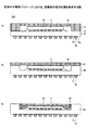
図1は、従来の半導体パッケージにおける、放熱板の使用状態を例示する図である。図1の(a)に、半導体素子11を収容する凹部12を有し、サーマルグリス13を通して半導体素子11から流入してくる熱流を表面から放熱するための放熱板14を示す。放熱板14は、接着剤15により基板16に固定されて、半導体パッケージ100を形成している。基板16の、半導体素子11の反対側の面16aの接続端子17には、はんだボール18が接続されており、マザーボード等の他の基板に接続されるための外部接続端子を形成する。
FIG. 1 is a diagram illustrating a use state of a heat sink in a conventional semiconductor package. FIG. 1A shows a
図の(b)は、中央に凹型領域19を有する基板20と組み合わせて用いられる平板の放熱板21を有する半導体パッケージの例である。図の(c)は、基板23の中央の凹型領域22に埋め込まれた、平板の放熱板24を有する半導体パッケージを示している。凹型領域22における半導体素子11の占める空間以外の空間部分は、封止材料22により充填されている(特許文献1)。
(B) of the figure is an example of a semiconductor package having a
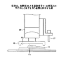
図2は、従来の、放熱板26と半導体素子11の背面との平行出しと接合を行う装置を例示する図である。この装置による平行出しは、以下の通りに行う。センサ27を用いて、半導体素子11の背面11bとその面に対向する放熱板26の面26aとの距離を光反射等により平行状態を測定する。測定結果に基づき、平行出し機構28を用いて、放熱板26を位置制御し、接合面11bと26aとの平行度を所定の値にして、半導体素子11に接合する。平行出し機構28の摺動機構には、エアーベアリング等が使用される(特許文献2)。
FIG. 2 is a diagram exemplifying a conventional apparatus for parallelizing and joining the
従来の、放熱板を有する半導体パッケージの組立ての製造においては、半導体素子の背面と、その面と対向する放熱板の面との平行状態を保つため、製造において、複雑な構造の設備を使用し、また、複雑な工程を要していた。そのため、生産工程の簡素化、生産コストの低減及び品質の向上に課題を有していた。 In the conventional manufacturing of the assembly of a semiconductor package having a heat sink, in order to maintain the parallel state between the back surface of the semiconductor element and the surface of the heat sink facing the surface, equipment having a complicated structure is used. In addition, complicated processes were required. For this reason, there are problems in simplifying the production process, reducing production costs, and improving quality.
上記目的を達成するため、第1の発明は、配線基板に搭載された半導体素子に、前記半導体素子との接合面と反対側の面の一部又は全部に凸状曲面の部分を形成した半導体素子用放熱板を載置する放熱板載置工程と、平面を有する押圧板の平面部を、前記凸状曲面の部分に押し付けて、前記半導体素子用放熱板を前記半導体素子に押付けることにより、自動的に前記半導体素子用放熱板と前記半導体素子との面合せを行う自動面合せ工程とを有する半導体パッケージの製造方法を提供する。 To achieve the above object, according to a first aspect of the present invention, there is provided a semiconductor device in which a convex curved surface is formed on a part or all of a surface opposite to a bonding surface with the semiconductor device on a semiconductor device mounted on a wiring board. A heat sink mounting step for mounting the element heat sink, and a flat surface portion of the pressing plate having a flat surface is pressed against the convex curved portion, and the semiconductor element heat sink is pressed against the semiconductor element. And a method of manufacturing a semiconductor package, which includes an automatic surface matching step of automatically aligning the semiconductor element heat sink and the semiconductor element.
また、上記目的を達成するため、第2の発明は、半導体素子を搭載した配線基板と、半導体素子用放熱板とを有し、前記半導体素子用放熱板は、前記半導体素子に接合され、かつ、半導体素子との接合面と反対側の面の一部又は全部に、凸状曲面の部分を形成している半導体パッケージを提供する。 In order to achieve the above object, the second invention includes a wiring board on which a semiconductor element is mounted, and a semiconductor element heat sink, the semiconductor element heat sink being joined to the semiconductor element, and Provided is a semiconductor package in which a convex curved portion is formed on a part or all of a surface opposite to a bonding surface with a semiconductor element.
本発明により、半導体パッケージの放熱板組立において、生産工程を簡素化し、生産コストを低減し、品質の向上を図ることができる。 According to the present invention, in the heat sink assembly of a semiconductor package, the production process can be simplified, the production cost can be reduced, and the quality can be improved.
以下、図面を参照して、本発明を実施するための最良の実施の形態を説明する。なお、各図の説明において、各図に共通している同一構成部分については、その部分に同一の符号を付し、重複する場合にはその説明を省く。 The best mode for carrying out the present invention will be described below with reference to the drawings. In the description of each figure, the same components common to each figure are denoted by the same reference numerals, and the description thereof is omitted when overlapping.
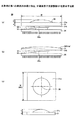
〈第1の実施の形態〉
図3は、本発明の第1の実施の形態に係る半導体素子用放熱板31を例示する図である。半導体素子用放熱板31の、半導体素子32に対向する面31bは、接合層33を介して半導体素子32と接合されている。半導体素子用放熱板31は、放熱側の面31aの一部分または全部に、滑らかな凸状曲面の部分34を形成している。放熱側の面31aの中央部に設け、盛り上がった凸形状、または、なだらかな曲面の凸形状等、種々の形状とすることができる。通常、放熱側の面31aの中央部の位置に凸形状の最高地点を置く。また、凸状曲面の製作上の都合等で、凸状曲面の裾野の部分は、凹状曲面を呈していてもよい。
<First Embodiment>
FIG. 3 is a diagram illustrating a semiconductor element
熱放散を要する半導体パッケージの構造において、半導体素子と半導体素子用放熱板とが、片当たりすることなく平行度を保って放熱の効率を上げることが重要である。両者の平行度を精度よく保つため、製造方法として「自動面合せ」を行う。この自動面合せのため、凸状曲面の部分を有する半導体素子用放熱板を使用する。 In the structure of a semiconductor package that requires heat dissipation, it is important that the semiconductor element and the heat dissipation plate for the semiconductor element maintain parallelism without being in contact with each other and increase the efficiency of heat dissipation. In order to maintain the parallelism between the two with high accuracy, “automatic matching” is performed as a manufacturing method. For this automatic matching, a heat sink for a semiconductor element having a convex curved surface portion is used.
図3の(a)は、半導体素子用放熱板31の放熱側の面31aの一部分が凸状曲面の部分34をなし、かつ、面31aの他の部分が平面である場合を示している。
FIG. 3A shows a case where a part of the heat
図3の(b)においては、放熱側の面31aの全体が凸状曲面の部分34をなす場合を示している。
FIG. 3B shows a case where the
ここに、「自動面合せ」とは、放熱板と半導体素子を接合する際に、プレス機械の押圧板の平坦な面が、放熱板の凸状曲面の部分を押すことにより、放熱板が自動的に回転して、放熱板及び半導体素子の各接合面の平行度を得る方法である。その詳細は、後出の〈第3の実施の形態〉で説明する。 Here, “automatic surface alignment” means that when the heat sink and the semiconductor element are joined, the flat surface of the pressing plate of the press machine presses the convex curved surface of the heat sink, so that the heat sink automatically The parallelism of each joint surface of a heat sink and a semiconductor element is obtained. Details thereof will be described later in <Third Embodiment>.
図3における接合層33を構成する物質は、熱伝導性を示唆して、TIM(Thermal Interface Material)と呼ばれ、樹脂としては、例えば、シリコンポリマー系樹脂が用いられる。その他、TIMには、インジウム、インジウムの合金等の金属、カーボンを含有した樹脂又はカーボンを含有した金属等を使用することができる。
The material constituting the
半導体素子用放熱板の形状寸法としては、例えば、図3の(c)の平面視した形状について、1辺の長さWが15〜60mmの正方形、または、長辺の長さW1が15〜60mmの長方形で、厚さdは、1〜3mmである。凸状曲面の部分の高さhは、例えば、1辺の長さWが40mmの正方形の場合に、40μmである。 As a shape dimension of the heat sink for semiconductor elements, for example, in the shape of FIG. 3C in plan view, a square having a side length W of 15 to 60 mm, or a long side length W1 of 15 to 15 mm. It is a rectangle of 60 mm, and the thickness d is 1 to 3 mm. The height h of the convex curved surface portion is, for example, 40 μm when the length W of one side is 40 mm.
放熱板の材質としては、例えば、熱伝導性に優れた無酸素銅C1020、銀、アルミニウム、または、それらの合金等を使用する。 As the material of the heat sink, for example, oxygen-free copper C1020 having excellent thermal conductivity, silver, aluminum, or an alloy thereof is used.
放熱板の製造は、鍛造加工、機械切削等により行われる。 The heat sink is manufactured by forging, machine cutting, or the like.
図3において、半導体素子32が搭載されている配線基板35の形態の例は、PGA(Pin Grid Array)である。配線基板35の形態は、PGAに限らず、LGA(Land Grid Array)またはBGA(Ball Grid Array)等の形態でもよく、また、電子応用機器に使用されるマザーボード等の配線基板であってもよい。
In FIG. 3, the example of the form of the
なお、図3の配線基板35の半導体素子32側の面上において、配線基板35と半導体素子用放熱板31との間隙の部分には、チップコンデンサ等の受動部品または他の半導体素子等が搭載される場合もある。
On the surface of the
〈第1の実施の形態の効果〉
半導体パッケージの製造において、半導体素子と半導体素子用放熱板との自動面合せを可能にする機構を提供して、半導体素子用放熱板31と半導体素子32との接合面間の平行度を容易に確保することができ、半導体素子の放熱効果を高めることができる。従って、品質の向上及び生産性の向上を図ることができる。
<Effect of the first embodiment>
In the manufacture of a semiconductor package, a mechanism that enables automatic matching between a semiconductor element and a semiconductor element heat sink is provided, and the parallelism between the joining surfaces of the semiconductor
〈第1の実施の形態の変形例〉
本発明の第1の実施の形態の変形例は、半導体素子用放熱板の凸状曲面の部分の材料が、半導体素子用放熱板の他の部分の材料と異なる半導体素子用放熱板の例である。材料としては、プレス機械からの押付け力に耐えることのできる金属、または樹脂を使用することできる。樹脂を使用する場合には、半導体素子用放熱板の面31aの中央部36(図3の(c))に、樹脂を塗布して滑らかな曲面の盛り上がった形状等を形成し、硬化させた後、自動面合せを行う。そして、半導体素子用放熱板と半導体素子との相互位置関係を定めた後に、その樹脂を削除してもよい。樹脂等の削除により、放熱面31aを平坦にする場合、例えば、接合面が平坦な放熱フィンを接合する場合等に、樹脂削除の方法を利用することができる。
<Modification of First Embodiment>
The modification of the first embodiment of the present invention is an example of a heat sink for a semiconductor element in which the material of the convex curved portion of the heat sink for the semiconductor element is different from the material of the other part of the heat sink for the semiconductor element. is there. As the material, a metal that can withstand the pressing force from the press machine, or a resin can be used. In the case of using a resin, the resin is applied to the central portion 36 (FIG. 3C) of the
〈第1の実施の形態の変形例の効果〉
自動面合せを行った後、放熱面が平坦な半導体素子用放熱板を得ることができる。接合面に平坦性を必要とする放熱フィン機構等の取り付けに、特に有効である。
<Effects of Modification of First Embodiment>
After performing automatic surface matching, a heat dissipation plate for a semiconductor element having a flat heat dissipation surface can be obtained. This is particularly effective for attaching a heat dissipating fin mechanism or the like that requires flatness on the joint surface.
〈第2の実施の形態〉
図4は、本発明の第2の実施の形態に係る、半導体素子を搭載した配線基板と半導体素子用放熱板とを有する、半導体パッケージを例示する図である。半導体パッケージは、半導体素子を囲むような形状の凹部を放熱板の半導体素子側の面に有し、または、配線基板にキャビティ(凹型領域)を有したパッケージである。
<Second Embodiment>
FIG. 4 is a diagram illustrating a semiconductor package having a wiring board on which a semiconductor element is mounted and a semiconductor element heat dissipation plate according to the second embodiment of the present invention. The semiconductor package is a package that has a concave portion that surrounds the semiconductor element on the surface of the heat dissipation plate on the semiconductor element side or that has a cavity (concave area) in the wiring board.
図4の(a)は、半導体素子32の占有空間を確保するための凹部41を有する、半導体素子用放熱板42aを特徴とする半導体パッケージである。(b)は、半導体素子32を収容するキャビティ43を有する配線基板45bの周縁部44と接合している、平板の半導体素子用放熱板42bを特徴とし、(c)は、半導体素子32を収容するキャビティ43内に設けられた、平板の半導体素子用放熱板42cを特徴としている。
FIG. 4A shows a semiconductor package characterized by a semiconductor element
図4の(a)の半導体パッケージにおいて、半導体素子32の背面32aと、半導体素子用放熱板42aの対向面46aとは、接合層33で接合され、半導体素子用放熱板42aと配線基板45aとは接合層47で接合されている。接合層33及び47の材料としては、シリコンポリマー系の樹脂が使用される。
In the semiconductor package of FIG. 4A, the
半導体素子用放熱板の寸法としては、例えば、凹部41を形成する周壁48の幅Dが2〜3mm、凹部41の深さCaが、0.5〜0.9mmである。
As a dimension of the heat sink for semiconductor elements, for example, the width D of the
図4の(a)における凹部41の深さCaの値は、半導体素子32の厚さ、接合層33の厚さ及びバンプ49等の高さを合計した値より、小さく設定することができる。この寸法の設定により、半導体素子用放熱板42aは、その周壁48を対向する配線基板45aに突き当てることなく、半導体素子32の背面32aと対向面46aとが平行となるように、優先的に回転することができる。従って、「自動面合せ」が容易になる。なお、半導体素子32等の厚さの合計値と、凹部41の深さCaの値との差により、半導体素子用放熱板42aの周壁48と配線基板45aとに隙間を生じるが、接合層47の厚さを適宜選んで、接合層47を間隙に十分に充填させることができる。従って、半導体素子用放熱板42aの周壁48と配線基板45aとを確実に接合することができる。
The value of the depth Ca of the
図4の(b)におけるキャビティ43の深さCbの値についても、上記の凹部41のCaと同様に、半導体素子32の厚さ、接合層33の厚さ及びバンプ49等の高さを合計した値より、小さく設定することができ、半導体素子用放熱板42bの優先的な回転が確保でき、「自動面合せ」を行うことができる。また、接合層47を十分に充填させることにより、半導体素子用放熱板42bと配線基板45bの周縁部44とを確実に接合することができる。
As for the value of the depth Cb of the
なお、図4の(a),(b)及び(c)について、配線基板45a,45b及び45cの形態は、PGAの例を示したが、LGA、BGAまたはマザーボード等を使用することができる。
4 (a), (b), and (c), the
〈第2の実施の形態の効果〉
半導体素子用放熱板が凹部を有し、または、配線基板がキャビティを有する場合の、半導体素子と半導体素子用放熱板との接合は、これらの閉空間における接合であるため、従来の、接合面の相互距離把握と接合の押付け方向の設定は困難を伴うものであった。半導体素子の側面からの接合部位の計測、測定が困難であったからである。しかし、本発明の、凸状曲面の部分を有する半導体素子用放熱板を使用すれば、容易に自動面合せを行うことができるので、一連の高精度の接合の工程を容易に実施することができ、放熱効果の優れた半導体パッケージを得ることができる。従って、品質の向上、生産性の向上を図ることができる。
<Effects of Second Embodiment>
When the semiconductor element heat sink has a recess or the wiring board has a cavity, the bonding between the semiconductor element and the semiconductor element heat sink is a bond in these closed spaces. It was difficult to determine the mutual distance and to set the pressing direction of the joint. This is because it is difficult to measure and measure the bonded portion from the side surface of the semiconductor element. However, if a heat sink for a semiconductor element having a convex curved surface according to the present invention is used, automatic mating can be easily performed, so that a series of high-precision joining steps can be easily performed. And a semiconductor package having an excellent heat dissipation effect can be obtained. Therefore, it is possible to improve quality and productivity.
〈第3の実施の形態〉
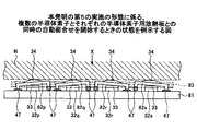
本発明の第3の実施の形態は、自動面合せ工程を有する半導体パッケージの製造方法の例である。
<Third Embodiment>
The third embodiment of the present invention is an example of a method for manufacturing a semiconductor package having an automatic surface matching process.
(自動面合せと片当たり)
本発明に係る「自動面合せ」は、半導体素子と半導体素子用放熱板のおのおのの接合面を相互に平行の位置に定めるための方法で、プレス機械等に測定、制御の機構を設けることなく、プレス機械等の押付け力のみによって、接合すべき対象部品が自動的に作動し、いわば、self−alignment(自動調芯)ともいうべき動作によって、接合面の平行度を出す方法である。
(Automatic matching and per piece)
“Automatic matching” according to the present invention is a method for determining the joint surfaces of a semiconductor element and a heat sink for semiconductor elements at positions parallel to each other, without providing a measurement and control mechanism in a press machine or the like. In other words, the target parts to be joined are automatically operated only by the pressing force of a press machine or the like. In other words, this is a method in which the parallelism of the joining surfaces is obtained by an operation that should be called self-alignment.
図5は、本発明の第5の実施の形態に係る半導体パッケージの製造方法における「自動面合せ」を説明する図である。なお、自動面合せの動きの理解を容易にするため、図の一部は誇張されている。 FIG. 5 is a diagram for explaining “automatic matching” in the method of manufacturing a semiconductor package according to the fifth embodiment of the present invention. Note that a part of the drawing is exaggerated in order to facilitate understanding of the movement of the automatic surface matching.
図5の(a)は、半導体素子用放熱板31と半導体素子32の各接合面31bと32aとが平行である状態を示す。
FIG. 5A shows a state in which the semiconductor element
図5の(b)は、接合面31bと32aとが平行でなく、半導体素子の接合面32aの左端P点、中央Q点、右端R点のうち、P点の箇所が、接合層33を介して、半導体素子用放熱板31上に片当たりしている状態を示している。片当たりは、半導体素子用放熱板31の接合面31bと半導体素子32の接合面32aとが平行でない結果、生じる。平行でないのは、測定または接合の動作に起因する。具体的には、例えば、半導体素子用放熱板31の厚さの不均一性、プレス機械等の押付け力の方向のずれ等いくつかの要因によるものである。製造の過程で、それぞれの要因を個別に解決することは困難である。また、仮に、片当たりした状態で半導体素子と半導体素子用放熱板とが接合された場合には、未接合部分の空間またはボイドが生じて、放熱機能が十分でなく接合強度を有しない半導体パッケージとなる。従って、各接合面間の片当たり状態を避け、平行出しをすることが重要である。
In FIG. 5B, the bonding surfaces 31 b and 32 a are not parallel, and the point P among the left end P point, the center Q point, and the right end R point of the
(片当たり時の半導体素子用放熱板の動き)
図5の(b)に示す片当たりの状態になり、押付け力がかかると、半導体素子接合面32aの、点Pの箇所の接合層33が圧迫される。流動性を有する接合層33は、点Pの箇所における肉厚が減少して、半導体素子用放熱板31と半導体素子32とが点Pにおいてほぼ接した状態となり、点Pにおいて、両者間に強い反力が発生する。点Pにおいて片当たりしている一方で、点Q、R付近においては反力が発生せず、無負荷状態となる。半導体素子用放熱板31の全体は、プレス機械の押圧板Nにより、矢印Xの方向に押されているので、半導体素子用放熱板31が受ける偶力のモーメントの釣り合いが崩れる。すると、半導体素子用放熱板31は、点Pを中心として、矢印Aの方向に回転し始める。そして、この回転の動きは、接合面間が平行となって、偶力のモーメントが釣り合いの状態となるまで継続する。すなわち、図5の(a)に示すような半導体素子用放熱板31の面31bが、半導体素子32の面32aに平行な状態となるまで、継続する。平行状態においては、接合面における矢印Xの方向の発生応力は、点P,Q,Rを含め、ほぼ全ての点において、等しくなり、半導体素子用放熱板31にかかる力の偶力のモーメントが釣り合うこととなる。さらに、プレス機械等によるX方向の押付け力によって、接続層33の粘度等の物性値に応じて、半導体素子用放熱板の面31bと半導体素子の面32aとの面間距離が定まる。以上のように、半導体素子の面と半導体素子用放熱板の面との平行度の自動調整を、プレス機械等に、測定、制御の機構を設けることなく、行わせることができる。
(Movement of heat sink for semiconductor element when hitting one piece)
5B, when the pressing force is applied, the
なお、接合層が流動性を有する場合について、半導体素子用放熱板の動きを説明したが、接合層の材料が金属等のような硬い場合であっても、半導体素子用放熱板にかかる力の偶力のモーメントが釣り合う状態は同様であり、半導体素子の面と半導体素子用放熱板の面との「自動面合せ」を行うことができる。 Although the movement of the semiconductor element heat sink has been described for the case where the bonding layer has fluidity, the force applied to the semiconductor element heat sink may be reduced even when the bonding layer material is hard, such as metal. The state in which the moments of the couple are balanced is the same, and “automatic matching” between the surface of the semiconductor element and the surface of the heat sink for the semiconductor element can be performed.
(半導体パッケージの製造方法)
図6は、本発明の第3の実施の形態に係る、半導体パッケージの製造方法の工程を例示する図である。工程は、ステップ1.放熱板載置工程(S101)、ステップ2.自動面合せ工程(S102)、ステップ3.接合層硬化工程(S103)を有している。半導体パッケージの構造として、図3の(a)の例を参照して説明する。
(Semiconductor package manufacturing method)
FIG. 6 is a diagram illustrating the steps of the semiconductor package manufacturing method according to the third embodiment of the invention. The process consists of step 1. 1. Heat sink mounting step (S101), step 2. 2. Automatic surface matching step (S102), step 3. It has a joining layer hardening process (S103). The structure of the semiconductor package will be described with reference to the example of FIG.
(ステップ1.放熱板載置工程)
半導体素子を搭載した配線基板35を準備して、半導体素子32の放熱面(通常集積回路面の裏面)32aに接合層33を塗布する。接合層33の部材は、TIMといい、例えば、シリコンポリマー系樹脂を使用する。TIMを塗布し半硬化状態とする手順は、周知の樹脂塗布技術に従う。次に、TIMが塗布された半導体素子32に、凸状曲面の部分34を形成した半導体素子用放熱板31を載置する。その他、TIMには、インジウム、インジウムの合金等の金属、カーボンを含有した樹脂又はカーボンを含有した金属等を使用することができる。TIMが流動性を有しない硬い材料の場合であっても、工程を進めることができる。
(Step 1. Heat sink mounting process)
A
(ステップ2.自動面合せ工程)
プレス機械等(図示せず)を用いて、半導体素子用放熱板31を半導体素子32の側に向かって押付け、自動面合せを行う。自動面合せについては、前出の〈第3の実施の形態〉において詳説したので、説明を省く。
(Step 2. Automatic mating process)
Using a press machine or the like (not shown), the semiconductor element
(ステップ3.接合層硬化工程)
周知の樹脂硬化技術に従って、接合層の硬化を行う。図4の半導体パッケージの例に示されているように、半導体素子用放熱板が、半導体素子との接合層33以外に、配線基板との接合層47等を有している場合には、接合層47等の肉厚を確保しながら、半導体素子との自動面合せを行う。半導体パッケージにおける接合層47の肉厚の値は、例えば、0.2〜0.25mmである。
(Step 3. Bonding layer curing process)
The bonding layer is cured according to a known resin curing technique. As shown in the example of the semiconductor package in FIG. 4, when the semiconductor element heat sink has a
〈第3の実施の形態の効果〉
自動面合せ、すなわち、半導体素子の接合面と半導体素子用放熱板の接合面との平行度の自動調整を、プレス機械等に測定、制御の機構を設けることなく、行わせることができる。従って、生産性の向上及び品質の向上を図ることができる。
<Effect of the third embodiment>
Automatic surface matching, that is, automatic adjustment of the parallelism between the bonding surface of the semiconductor element and the bonding surface of the heat sink for the semiconductor element can be performed without providing a measurement and control mechanism in the press machine or the like. Accordingly, productivity and quality can be improved.
〈第4の実施の形態〉
図7は、本発明の第4の実施の形態に係る、半導体素子用放熱板71に放熱フィン72を設けた半導体パッケージ70を例示する図である。放熱フィン72の接合により、半導体素子の放熱の熱効率を、さらに高めることができる。放熱フィン72については、周知の種々の形状、材質を使用することができる。
<Fourth embodiment>
FIG. 7 is a diagram illustrating a
放熱フィン72と半導体素子用放熱板71の放熱面71aとの接合層73の材料としては、シート状またはジェル状のTIM、例えばシリコンポリマー系樹脂が用いられる。
As a material of the
さらに、放熱フィン72の上面に冷却ファン74を設けることにより、空気の強制対流等によって、放熱の熱効率を上げることができる。
Furthermore, by providing the cooling
〈第4の実施の形態の効果〉
半導体素子用放熱板のみの放熱機構と比較して、さらに高い放熱の熱効率を得ることができ、製品性能の向上を図ることができる。
<Effect of the fourth embodiment>
Compared with a heat dissipation mechanism using only a heat sink for semiconductor elements, higher heat dissipation thermal efficiency can be obtained, and product performance can be improved.
〈第5の実施の形態〉
本発明の第5の実施の形態は、配線基板上に2次元配列した複数の半導体素子に対して半導体素子用放熱板の自動面合せ及び接合を行う、半導体パッケージの製造方法の例である。製造工程は、〈第3の実施の形態〉における工程と、半導体素子の個数以外は同様であるので、詳細の説明を省く。
<Fifth embodiment>
The fifth embodiment of the present invention is an example of a method for manufacturing a semiconductor package, in which a semiconductor element heat sink is automatically faced and joined to a plurality of semiconductor elements arranged two-dimensionally on a wiring board. The manufacturing process is the same as that in <Third Embodiment> except for the number of semiconductor elements, and thus detailed description thereof is omitted.
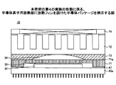
図8は、本発明の第5の実施の形態に係る半導体パッケージの製造方法について、複数の半導体素子32p,32q,32r及び32sと、それぞれに対応する半導体素子用放熱板82p,82q,82r及び82sとの同時の自動面合せを開始するときの状態を例示する図である。半導体素子用放熱板のそれぞれの凸状曲面の部分34が、プレス機械の押圧板Nに接触して、矢印Xの方向に押付け力を受けている状態である。
FIG. 8 shows a semiconductor package manufacturing method according to the fifth embodiment of the present invention, in which a plurality of
半導体素子用放熱板82p等が載置されたままの状態から、プレス機械の押圧板Nにより、個々に押付け力を受けて、半導体素子32p等の面との平行度の自動調整が開始される。このようにして、個々の半導体素子用放熱板を、同時に、自動面合せすることができる。自動面合せについては、前出の〈第3の実施の形態〉及び図5の(a)と(b)により説明した内容と重複するので、その記載を省く。
From the state in which the semiconductor element
なお、同時自動面合せの際に、半導体素子用放熱板82p等の、配線基板81の平面の方向等へのずれが予想される場合には、例えば、リテーナ(支持枠)83を使用すれば、そのずれを防ぐことができる。
In the case of simultaneous automatic face-to-face matching, if a shift of the semiconductor
〈第5の実施の形態の効果〉
複数の半導体素子に対し、同時に、半導体素子用放熱板の自動面合せを行い、接合を行うことができるので、生産性の向上及び製造コストの削減を図ることができる。
<Effect of Fifth Embodiment>
Since a semiconductor element heat sink can be automatically faced and bonded to a plurality of semiconductor elements at the same time, productivity can be improved and manufacturing costs can be reduced.
〈本発明に係る他の実施の形態〉
以上、本発明の好ましい実施の形態について詳説したが、本発明は、上述した実施の形態に制限されることはなく、本発明の範囲を逸脱することなく、上述した実施の形態に種々の変形及び置換を加えることができる。
<Other Embodiments According to the Present Invention>
The preferred embodiment of the present invention has been described in detail above. However, the present invention is not limited to the above-described embodiment, and various modifications can be made to the above-described embodiment without departing from the scope of the present invention. And substitutions can be added.
30,70 半導体パッケージ
31,42a,42b,42c,71,82p,82q,82r,82s 半導体素子用放熱板
31a 放熱側の面
31b 半導体素子用放熱板31の、半導体素子32に対向する面
32,32p,32q,32r,32s 半導体素子
32a 半導体素子32の半導体素子用放熱板との接合面
33,47,73 接合層
34 凸状曲面の部分
35,45a,45b,45c,81 配線基板
41 凹部
43 キャビティ
44 配線基板45bのキャビティ43の周縁部
48 半導体素子用放熱板42aの凹部41を形成する周壁
49 バンプ
71a 半導体素子用放熱板71の放熱面
72 放熱フィン
74 冷却ファン
83 リテーナ(支持枠)
Ca 凹部41の深さ
Cb キャビティ43の深さ
D 周壁48の幅
N プレス機械の押圧板
P,Q,R 半導体素子の接合面の点
30, 70 Semiconductor packages 31, 42a, 42b, 42c, 71, 82p, 82q, 82r, 82s Semiconductor element
Claims (7)
平面を有する押圧板の平面部を、前記凸状曲面の部分に押し付けて、前記半導体素子用放熱板を前記半導体素子に押付けることにより、自動的に前記半導体素子用放熱板と前記半導体素子との面合せを行う自動面合せ工程とを有する半導体パッケージの製造方法。 A heat dissipating plate mounting step for mounting a heat dissipating plate for a semiconductor element in which a convex curved surface portion is formed on a part or all of the surface opposite to the bonding surface with the semiconductor element on a semiconductor element mounted on a wiring board When,
By pressing the flat portion of the pressing plate having a flat surface against the convex curved surface portion and pressing the semiconductor element heat dissipation plate against the semiconductor element, the semiconductor element heat dissipation plate and the semiconductor element are automatically A method of manufacturing a semiconductor package, comprising: an automatic surface matching step for performing surface matching.
半導体素子用放熱板とを有し、
前記半導体素子用放熱板は、前記半導体素子に接合され、かつ、半導体素子との接合面と反対側の面の一部又は全部に、凸状曲面の部分を形成している半導体パッケージ。 A wiring board on which a semiconductor element is mounted;
A heat sink for semiconductor elements,
The semiconductor element heat radiation plate is bonded to the semiconductor element, and a convex curved surface portion is formed on a part or all of the surface opposite to the bonding surface with the semiconductor element.
Priority Applications (2)
| Application Number | Priority Date | Filing Date | Title |
|---|---|---|---|
| JP2009195737A JP2011049311A (en) | 2009-08-26 | 2009-08-26 | Semiconductor package and manufacturing method |
| US12/861,008 US20110049702A1 (en) | 2009-08-26 | 2010-08-23 | Semiconductor package and method of producing the same |
Applications Claiming Priority (1)
| Application Number | Priority Date | Filing Date | Title |
|---|---|---|---|
| JP2009195737A JP2011049311A (en) | 2009-08-26 | 2009-08-26 | Semiconductor package and manufacturing method |
Publications (2)
| Publication Number | Publication Date |
|---|---|
| JP2011049311A true JP2011049311A (en) | 2011-03-10 |
| JP2011049311A5 JP2011049311A5 (en) | 2012-09-06 |
Family
ID=43623617
Family Applications (1)
| Application Number | Title | Priority Date | Filing Date |
|---|---|---|---|
| JP2009195737A Pending JP2011049311A (en) | 2009-08-26 | 2009-08-26 | Semiconductor package and manufacturing method |
Country Status (2)
| Country | Link |
|---|---|
| US (1) | US20110049702A1 (en) |
| JP (1) | JP2011049311A (en) |
Families Citing this family (5)
| Publication number | Priority date | Publication date | Assignee | Title |
|---|---|---|---|---|
| CN103954260A (en) * | 2014-05-28 | 2014-07-30 | 苏州艾酷玛赫设备制造有限公司 | Automobile radiator detecting device |
| US10607857B2 (en) | 2017-12-06 | 2020-03-31 | Indium Corporation | Semiconductor device assembly including a thermal interface bond between a semiconductor die and a passive heat exchanger |
| TR201816893A2 (en) * | 2018-11-09 | 2019-02-21 | Kale Oto Radyatoer Sanayi Ve Ticaret Anonim Sirketi | Multi-Row Tubular Automatic Radiator Lining Machine |
| US11710677B2 (en) * | 2019-07-08 | 2023-07-25 | Intel Corporation | Ultraviolet (UV)-curable sealant in a microelectronic package |
| US11842944B2 (en) * | 2019-12-26 | 2023-12-12 | Intel Corporation | IC assemblies including die perimeter frames suitable for containing thermal interface materials |
Citations (8)
| Publication number | Priority date | Publication date | Assignee | Title |
|---|---|---|---|---|
| JPH01220852A (en) * | 1988-02-29 | 1989-09-04 | Hitachi Ltd | Semiconductor device |
| JPH0269962A (en) * | 1988-09-05 | 1990-03-08 | Sumitomo Electric Ind Ltd | Manufacture of semiconductor device |
| JPH06112350A (en) * | 1992-09-30 | 1994-04-22 | Mitsubishi Electric Corp | Semiconductor device |
| JP2005217295A (en) * | 2004-01-30 | 2005-08-11 | Renesas Technology Corp | Manufacturing method of semiconductor device |
| JP2006049732A (en) * | 2004-08-09 | 2006-02-16 | Sony Corp | Manufacturing method and manufacturing apparatus of semiconductor package |
| WO2007084572A2 (en) * | 2006-01-18 | 2007-07-26 | Honeywell International Inc. | Thermal interconnect and interface systems, methods of production and uses thereof |
| JP2008244473A (en) * | 2007-03-26 | 2008-10-09 | Endicott Interconnect Technologies Inc | Flexible electronic circuit package with stand-off and method for manufacturing the same |
| JP2008300561A (en) * | 2007-05-30 | 2008-12-11 | Renesas Technology Corp | Manufacturing method of semiconductor device |
Family Cites Families (13)
| Publication number | Priority date | Publication date | Assignee | Title |
|---|---|---|---|---|
| US5900675A (en) * | 1997-04-21 | 1999-05-04 | International Business Machines Corporation | Organic controlled collapse chip connector (C4) ball grid array (BGA) chip carrier with dual thermal expansion rates |
| US6288900B1 (en) * | 1999-12-02 | 2001-09-11 | International Business Machines Corporation | Warpage compensating heat spreader |
| JP3881488B2 (en) * | 1999-12-13 | 2007-02-14 | 株式会社東芝 | Circuit module cooling device and electronic apparatus having the cooling device |
| US7061102B2 (en) * | 2001-06-11 | 2006-06-13 | Xilinx, Inc. | High performance flipchip package that incorporates heat removal with minimal thermal mismatch |
| JP3868777B2 (en) * | 2001-09-11 | 2007-01-17 | 株式会社東芝 | Semiconductor device |
| US6748350B2 (en) * | 2001-09-27 | 2004-06-08 | Intel Corporation | Method to compensate for stress between heat spreader and thermal interface material |
| US6848172B2 (en) * | 2001-12-21 | 2005-02-01 | Intel Corporation | Device and method for package warp compensation in an integrated heat spreader |
| US20050155743A1 (en) * | 2002-06-28 | 2005-07-21 | Getz George Jr. | Composite heat sink with metal base and graphite fins |
| US6930884B2 (en) * | 2003-06-11 | 2005-08-16 | Hewlett-Packard Development Company, L.P. | Land grid array assembly using a compressive liquid |
| US7319591B2 (en) * | 2005-05-26 | 2008-01-15 | International Business Machines Corporation | Optimized thermally conductive plate and attachment method for enhanced thermal performance and reliability of flip chip organic packages |
| US20080157345A1 (en) * | 2006-12-29 | 2008-07-03 | Daoqiang Lu | Curved heat spreader design for electronic assemblies |
| US7737550B2 (en) * | 2007-08-30 | 2010-06-15 | International Business Machines Corporation | Optimization of electronic package geometry for thermal dissipation |
| US7795724B2 (en) * | 2007-08-30 | 2010-09-14 | International Business Machines Corporation | Sandwiched organic LGA structure |
-
2009
- 2009-08-26 JP JP2009195737A patent/JP2011049311A/en active Pending
-
2010
- 2010-08-23 US US12/861,008 patent/US20110049702A1/en not_active Abandoned
Patent Citations (8)
| Publication number | Priority date | Publication date | Assignee | Title |
|---|---|---|---|---|
| JPH01220852A (en) * | 1988-02-29 | 1989-09-04 | Hitachi Ltd | Semiconductor device |
| JPH0269962A (en) * | 1988-09-05 | 1990-03-08 | Sumitomo Electric Ind Ltd | Manufacture of semiconductor device |
| JPH06112350A (en) * | 1992-09-30 | 1994-04-22 | Mitsubishi Electric Corp | Semiconductor device |
| JP2005217295A (en) * | 2004-01-30 | 2005-08-11 | Renesas Technology Corp | Manufacturing method of semiconductor device |
| JP2006049732A (en) * | 2004-08-09 | 2006-02-16 | Sony Corp | Manufacturing method and manufacturing apparatus of semiconductor package |
| WO2007084572A2 (en) * | 2006-01-18 | 2007-07-26 | Honeywell International Inc. | Thermal interconnect and interface systems, methods of production and uses thereof |
| JP2008244473A (en) * | 2007-03-26 | 2008-10-09 | Endicott Interconnect Technologies Inc | Flexible electronic circuit package with stand-off and method for manufacturing the same |
| JP2008300561A (en) * | 2007-05-30 | 2008-12-11 | Renesas Technology Corp | Manufacturing method of semiconductor device |
Also Published As
| Publication number | Publication date |
|---|---|
| US20110049702A1 (en) | 2011-03-03 |
Similar Documents
| Publication | Publication Date | Title |
|---|---|---|
| JP5635247B2 (en) | Multi-chip module | |
| JP5387685B2 (en) | Manufacturing method of semiconductor device | |
| US7563651B2 (en) | Method of fabricating a substrate with a concave surface | |
| US7271480B2 (en) | Constraint stiffener design | |
| TW200411863A (en) | Flip-chip package | |
| US8334174B2 (en) | Chip scale package and fabrication method thereof | |
| TWI228806B (en) | Flip chip package | |
| JP2023175042A (en) | Method for manufacturing electronic component device and electronic component device | |
| US8823164B2 (en) | Heatsink attachment module | |
| JP2013243339A (en) | Electronic component, electronic module, and manufacturing method of these | |
| JP2011049311A (en) | Semiconductor package and manufacturing method | |
| US11658099B2 (en) | Flip chip curved sidewall self-alignment features for substrate and method for manufacturing the self-alignment features | |
| US20170287873A1 (en) | Electronic assembly components with corner adhesive for warpage reduction during thermal processing | |
| TWI255488B (en) | Semiconductor device and multilayer substrate therefor | |
| JP2016162985A (en) | Semiconductor device manufacturing method | |
| US20090057866A1 (en) | Microelectronic Package Having Second Level Interconnects Including Stud Bumps and Method of Forming Same | |
| JP4335263B2 (en) | Semiconductor device and manufacturing method of semiconductor device | |
| US8237275B2 (en) | Tungsten stiffener for flexible substrate assembly | |
| TW200810050A (en) | Package structure and heat sink module thereof | |
| TWI253128B (en) | Method of manufacturing wafer level chip size package | |
| US20040075990A1 (en) | Packaging integrated circuits with adhesive posts | |
| JP2005064118A (en) | Semiconductor device and its manufacturing method | |
| JP2013012570A (en) | Semiconductor device and semiconductor device manufacturing method | |
| TWI271839B (en) | Chip package process and heat sink structure thereof | |
| JP2001144215A (en) | Flip-chip mounter |
Legal Events
| Date | Code | Title | Description |
|---|---|---|---|
| A521 | Written amendment |
Free format text: JAPANESE INTERMEDIATE CODE: A523 Effective date: 20120723 |
|
| A621 | Written request for application examination |
Free format text: JAPANESE INTERMEDIATE CODE: A621 Effective date: 20120723 |
|
| A977 | Report on retrieval |
Free format text: JAPANESE INTERMEDIATE CODE: A971007 Effective date: 20130109 |
|
| A131 | Notification of reasons for refusal |
Free format text: JAPANESE INTERMEDIATE CODE: A131 Effective date: 20130205 |
|
| A02 | Decision of refusal |
Free format text: JAPANESE INTERMEDIATE CODE: A02 Effective date: 20130910 |