JP2004363183A - Heat dissipating structure of electronic part - Google Patents
Heat dissipating structure of electronic part Download PDFInfo
- Publication number
- JP2004363183A JP2004363183A JP2003156919A JP2003156919A JP2004363183A JP 2004363183 A JP2004363183 A JP 2004363183A JP 2003156919 A JP2003156919 A JP 2003156919A JP 2003156919 A JP2003156919 A JP 2003156919A JP 2004363183 A JP2004363183 A JP 2004363183A
- Authority
- JP
- Japan
- Prior art keywords
- housing
- substrate
- heat
- gel
- layer
- Prior art date
- Legal status (The legal status is an assumption and is not a legal conclusion. Google has not performed a legal analysis and makes no representation as to the accuracy of the status listed.)
- Pending
Links
Images


Classifications
-
- H—ELECTRICITY
- H01—ELECTRIC ELEMENTS
- H01L—SEMICONDUCTOR DEVICES NOT COVERED BY CLASS H10
- H01L2924/00—Indexing scheme for arrangements or methods for connecting or disconnecting semiconductor or solid-state bodies as covered by H01L24/00
- H01L2924/0001—Technical content checked by a classifier
- H01L2924/0002—Not covered by any one of groups H01L24/00, H01L24/00 and H01L2224/00
Landscapes
- Cooling Or The Like Of Electrical Apparatus (AREA)
- Cooling Or The Like Of Semiconductors Or Solid State Devices (AREA)
Abstract
Description
【0001】
【発明の属する技術分野】
本発明は、電子部品の放熱構造に関する。より詳しくは、基板に素子をハンダ付けする電子部品における、素子の放熱効率を向上させるための放熱構造に関する。
【0002】
【従来の技術】
従来,半導体回路を設けた電子部品では、作動中の発熱を冷却して半導体回路動作を安定させる必要がある。電子部品としての半導体は一般に熱に弱く、温度変化により抵抗値やタイミング変化などが起こり誤動作することがある。このため、半導体素子の熱を排出して一定の温度範囲に維持する必要がある。
従来の素子の冷却構造としては、素子をはんだ付けにより絶縁基板上に配設し、この絶縁基板と放熱板とをはんだにより接続する。そして放熱板にシリコングリスを塗布して冷媒を保持する冷却ケースに取付けるものである。
このほかにも、素子直下の基板に大型のスルーホールを設けて基板下面に熱を導出したり、電子部品を覆うカバーを素子に当接させて熱を導出する構成が知られている(例えば、特許文献1を参照)。
また、多層配線基板において銅層を形成してヒートシンクに熱を導く構成(例えば、特許文献2を参照)や、素子の表面に金属箔をのせて、この金箔を介して封止キャップを当接させ、封止キャップに排熱させる構成も知られている(例えば、特許文献3を参照)。
【0003】
【特許文献1】
特開2002−151952号公報
【特許文献2】
特開平11―330708号公報
【特許文献3】
特開平11−121640号公報
【0004】
【発明が解決しようとする課題】
電子制御装置の小型化および高密度実装を考慮した場合に、基板内のパターン配線を微細化でき、表面ランドパターンの公差を小さくできることから、ガラスエポキシ基板を利用することが望まれている。しかしながら,通常のガラスエポキシ基板などの樹脂基板では、熱伝動性が低く放熱を効率的に行うことが困難である。
半導体素子において、素子本体の一側面は素子放熱板に取付けられており、他の部分はモールド樹脂により覆われている。一般的な素子の冷却構造において、素子はハンダにより樹脂基板上に取付けられ、樹脂基板にはアルミニウム製のヒートシンクが取付けられる。これらの熱伝導率は、それぞれ、モールド樹脂0.9W/m・K、素子本体2.6W/m・K、素子放熱板372W/m・K、はんだ36W/m・K、樹脂基板0.38W/m・K、アルミヒートシンク92W/m・Kである。ここにおいて、モールド樹脂と樹脂基板の熱伝導率が極端に低くく、放熱効率を低減する要因となっている。
このため、樹脂基板を用いた電子部品では、配設可能な雰囲気の温度範囲が狭、電子部品を配置可能な環境に制限がある。
【0005】
そして、特許文献1に記載された技術におけるスルーホールのみでの放熱では十分な放熱性を得ることができない。素子にカバーを当接させる場合においてもカバーと素子との取付け位置やカバーの成形精度など、高い精度が要求され、製造が困難となる。特許文献2、3においても同様に高い成形精度と組み付け精度が要求される。
【0006】
【課題を解決するための手段】
上記の課題を解決すべく、本発明は次のような手段を用いる。
請求項1に記載のごとく、素子を実装した基板を、放熱板とハウジングとで覆う電子部品の放熱構造において、該基板に放熱板に接続するサーマルビアを複数個形成し、該基板もしくは素子を基板に接続するハンダ層と、前記ハウジングとを放熱ゲルを介して接続した。
【0007】
請求項2に記載のごとく、素子を実装した基板を、放熱板とハウジングとで覆う電子部品の放熱構造において、該基板に放熱板に接続するサーマルビアを複数個形成するとともに、高熱伝導層を構成し、該高熱伝動層を基板表面に露出させ、該高熱伝動層とハウジングとを接続した。
【0008】
請求項3に記載のごとく、素子を実装した基板を、放熱板とハウジングとで覆う電子部品の放熱構造において、該基板に放熱板に接続するサーマルビアを複数個形成するとともに、高熱伝導層を構成し、該高熱伝動層を基板表面に露出させ、該高熱伝動層とハウジングとを接続し、基板に実装された素子とハウジングとの間に放熱ゲルを充填した。
【0009】
【発明の実施の形態】
次に、本発明の実施の形態について図を用いて説明する。
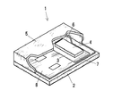
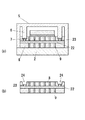
図1は電子制御ユニットの一部破断面図、図2は電子制御ユニットの組立て構成を示す斜視図、図3は電子制御ユニットの側面断面図である。
本実施例においては、電子部品の一例として、電子制御ユニットを用いて説明する。本発明に利用される電子部品としては、基板に素子を実装し、放熱板およびハウジングにより基板を覆うものであれば良く、特に限定されるものでははい。
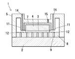
電子制御ユニット1は、素子4、基板8、放熱板2およびハウジング5により構成されている。素子4は基板8にハンダ付けにより取付けられており、素子4はハンダ層3を介して基板8に配設されている。基板8は放熱板2の上面に取付けられており、基板8の上方はハウジング5が配置される。放熱板2の上面縁部はハウジング5の下部に当接しており、ハウジング5の下部は基板8の外周縁に沿った形状となっている。これにより、基板8は、放熱板2とハウジング5とにより覆われる構成となっている。
【0010】
基板8において、ハンダ層3の下にはサーマルビア9が複数個構成されている。ハンダ層3は上部に配設される素子4より広く構成されており、平面視において素子4の周囲にハンダ層3が構成されている。このようにハンダ層を構成することで、ハンダ層3が基板8と接触する面積を拡大でき、素子が実装されていない部分にも熱を伝動させ、ハンダ層3を介した放熱量を増大させるものである。
そして、ハンダ層3を拡大することにより、サーマルビア9を配置可能な面積が増大できる。これにより、ハンダ層3と放熱板2とを接続する熱伝導度の高い経路を拡大して素子の放熱性を向上できる。
【0011】
ハウジング5の内側面には、当接部6が下方に延出されている。当接部6はハウジング5と一体的に構成されており、当接部6の下端部は平面視においてハンダ層3の縁部に沿った位置に構成されている。
ハンダ層3の縁部上面には放熱ゲル7が塗布されており、ハンダ層3と当接部6とは放熱ゲル7を介して接続する。放熱ゲルとしては、放熱シリコーンゲル等を利用するものである。
放熱ゲル7をハンダ層3と当接部6との間に配置させ、放熱ゲル7をハンダ層3と当接部6とに密着させる。これにより、ハンダ層3から当接部6への熱伝導経路を確保できる。放熱ゲル7は低硬度でありながら密着性が高く、粘性を有する。このため、振動や衝撃を受けた場合にも、放熱ゲルが塗布位置よりずれ難い。放熱ゲル7はハンダ層3の上面において塗布位置に保持され、ハンダ層3と当接部6とに密着して熱伝動経路を確保する。これにより、熱および振動に対しても熱伝導経路を安定して維持できる。
なお、放熱ゲル7としては熱伝導性の高いものを利用するものであり、高い熱伝動性を有するとともに、密着性、振動に対する位置の保持性能などが同様であれば他のものを利用することも可能である。
【0012】
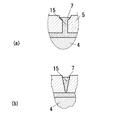
図4はハンダ層と当接部の位置関係を示す図であり、図4(a)は当接部が基準位置にある状態を、図4(b)は基準位置より高い状態を、図4(c)は基準位置より低い状態をそれぞれ示す図である。
放熱ゲル7をハンダ層3と当接部6との間に配設することにより、ハンダ層3と当接部6との位置が一定しない場合においてもハンダ層3と当接部6とを接続できるものである。
当接部6が図4(b)に示すごとく、基準位置より高い位置である場合にも放熱ゲル7の密着性および追従性によりハンダ層3と当接部6との接続が確保される。
また、図4(c)に示すごとく、当接部6が基準位置より低い位置にある場合においても、放熱ゲル7が低硬度であるという特性から、放熱ゲル7は変形しながらハンダ層3と当接部6との接続を行うものである。
そして、当接部6がさらに低い位置にある場合においても、ハンダ層3と当接部6の間において放熱ゲル7が当接部6のハンダ層3の押さえつけを緩和する。
すなわち、放熱ゲル7によりハンダ層3と当接部6との接続を確実にするとともに、基板8の保護も行うものである。そして、ハウジング5および素子4のハンダ付けにおいて高い精度を必要とせず、容易に素子4の放熱性の高い電子部品を構成することができる。また、ハンダ層3と当接部6の形状に関係なく、熱伝導経路を確保できる。
【0013】
次に、ハンダ層3と当接部6との接着性をさらに向上させる構成について、図5を用いて説明する。
図5はハンダ層と当接部との他の接続構成を示す図であり、図5(a)は当接部をハンダ層上面形状に沿わせた構成を示す図、図5(b)はハンダ層に凹部を構成した状態を示す図、図5(c)は当接部に突起を設けた構成を示す図である。
図5(a)に示す構成においては、当接部6の下端はハンダ層3の上面に沿った形状に構成されており、ハンダ層3の外側に向けて下がるように傾斜させているものである。当接部6の下面とハンダ層3の上面との間隔をほぼ一定にすることにより、放熱ゲル7と当接部6との接触面積を大きくし、放熱ゲル7の流動性を低減させ、保持性を向上させるものである。
【0014】
図5(b)に示す構成においては、ハンダ層3に、当接部6の下端形状にあわせた凹部を構成するものである。そして、この凹部に当接部6の下端を位置させることにより、放熱ゲル7とハンダ層3との接触面積を大きくし、放熱ゲル7の流動性を低減させ、保持性を向上させるものである。
図5(c)に示す構成においては、当接部6の下端に突起部を設ける物である。これにより、放熱ゲル7と当接部6との接触面積を大きくし、放熱ゲル7の流動性を低減させ、保持性を向上させるものである。さらに、当接部6がハンダ層3に接触した場合においても当接部6によりハンダ層3を変形させやすく基板8に影響を与えない。
【0015】
次に、図6から図10において放熱ゲルの接続性を確認する手段を設けたハウジングの構成について説明する。
図6は素子を放熱ゲルで覆う構成を示す断面図である。
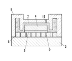
図6において、確認手段を設けた電子制御ユニットの全体構成について説明する。電子制御ユニット1のハウジング5は、素子4の上方に位置する部分を素子4に近づけた構成となっており、素子4の配置位置に相当する部分が凹んだ形状となっている。そして、素子4の側部を囲むようにハウジング5の内側面に延出部11が設けられている。延出部11はハウジング5内側面より下方に延出されている。
素子4は、延出部11および素子4の上方に位置するハウジング5により上面および側面を囲まれている。そして、素子4とハウジング5の間に放熱ゲル7が充填されている。素子4にハウジング5を近づけることにより、必要となる放熱ゲル7の量を低減でき、素子4の放熱効率を向上できる。
【0016】
ハウジング5には、延出部11の下端面からハウジング5上面にいたる位置確認用孔14が設けられており、位置確認用孔14の延長線上であって基板8上にマーク12が配置されている。図6において、位置確認用孔14は延出部11に沿って垂直方向に構成されており、延出部11の直下にマーク12が配設されている。
位置確認用孔14は、素子4に対するハウジング5の位置を確認するためのものである。位置確認用孔14によりマーク12が確認される場合には、ハウジング5の位置のズレが許容範囲であり、延出部11と素子4との間に隙間が存在することを示すものである。
これにより、素子4よりの放熱効率を向上させながら、電子制御ユニット1の組立て効率を向上できるものである。
【0017】
ハウジング5には、放熱ゲル7が充填される空間に連通する充填確認孔15が設けられている。図6において充填確認孔15は、ハウジング5の素子4直上位置に、垂直方向に設けられている。
充填確認孔15による、放熱ゲル7の充填確認方法について説明する。
図7は放熱ゲルが充填された状態を示す充填確認孔の構成を示す断面図である。図7に示すごとく、素子4とハウジング5との間に充填される放熱ゲル7は、充填確認孔15にも充填されるものである。充填確認孔15が放熱ゲル7により満たされるので、ハウジング5の外側より放熱ゲル7の状態を認識可能である。
【0018】
図8はゲル不足状態と充填状態とを示す模式図、図8(a)はゲル不足状態を示す図、図8(b)はゲルが十分な状態を示す図である。
図8に示すごとく、放熱ゲル4が不足している場合には、充填確認孔15が放熱ゲルにより満たされない。そして、素子4とハウジング5との間に放熱ゲル7が十分に充填されている場合には、充填確認孔15よりハウジング5の外面に放熱ゲル7が溢れ出し、外部より放熱ゲル7が十分に充填されていることを確認できるものである。ハウジング5より放熱ゲル7を溢れ出させるので、容易に放熱ゲル7の充填を認識できるものである。
【0019】
放熱ゲル7の充填を確認する充填確認孔15の構成としては、図8に示す構成の他にも様々なものを用いることができる。
図9は充填確認孔の他の構成例を示す図であり、図9(a)は上部をすり鉢状に構成した充填確認孔の構成を示す図、図9(b)は円錐状に構成した充填確認孔の構成を示す図である。
充填確認孔15の上部構成としては、図9(a)に示すごとく、上部をすり鉢上に構成することができる。これにより、放熱ゲル7があふれ出る前に、放熱ゲル7の露出面積を拡大して、認識しやすくできるものである。
また、図9(b)に示すごとく、充填確認孔15を円錐形状に構成することも可能である。充填確認孔15を円錐形状に構成することにより、放熱ゲル7の上面位置と界面面積とを対応させて、放熱ゲル7の界面位置を認識可能となるものである。
このほかに、充填確認孔15をハウジング5に複数個設けて、複数個所において放熱ゲル7の充填を確認することにより、放熱ゲル7の充填確認の確実性を向上できるとともに、部分的な放熱ゲル7の充填むらを認識可能である。
【0020】
充填確認孔15を設けたハウジング5において、ハウジング5内を放熱ゲル7により満たし、これを確認することも可能である。
図10はハウジング内を放熱ゲルにより満たした構成を示す図である。図10に示すごとく、ハウジング5は素子4の近傍において素子4の側方および上方を包むように構成されている。そして、下端部を放熱板2に当接させて、基板8をハウジング5および放熱板2により覆う。さらに、素子4を実装した基板8とハウジング5の間に放熱ゲル7を満たす。
これにより、放熱ゲル7を素子4および基板8の放熱部に接触させて、電子制御ユニット1の放熱性を向上できる。
なお、放熱ゲルを目視しやすくすべく、放熱ゲルに着色をしたり、充填確認孔15の内周面を着色したり、充填確認孔15周囲のハウジング5を着色することも可能である。
【0021】
次に、素子4を実装する基板に、高熱伝動率を有する層を設けて基板の熱伝導性を向上させる構成について説明する。この構成においては、基板内に熱伝動度の高い層を設け、この層を介して基板側部よりハウジングに熱を放出させるものである。ここにおいては、高熱伝導率層として銅層を用いる。
図11は基板に銅層を設けた構成を示す図である。
図11に示すごとく、基板8には銅層22が構成されている。銅層22は基板8の内層に埋め込む構成となっており、銅層22は基板8の側面に露出しているものである。銅層22は素子4実装部の直下および周囲に構成されたサーマルビア9・9・・に接続しており、サーマルビア9は基板8の上面から下面にかけて上下方向に構成されている。
銅層22を有する基板8は、下面を放熱板2の上面にあわせた状態で配設されており、基板8の側面および上面はハウジング5により覆われるものである。
【0022】
基板8の側面には放熱ゲル7が塗布されており、放熱ゲル7は基板8の側面およびハウジング5の内側面に密着している。これにより、基板8の銅層22が放熱ゲル7を介してハウジング5に接続する構成となる。これにより、素子4において発生した熱は、ハンダ層3、サーマルビア9、銅層22を介して、基板8の側面および下面に伝達され、ハウジング5および放熱板2より排熱される。
このように、基板8の側部を利用してハウジング5に熱を伝達するので、電子制御ユニットにおいて熱伝導性の高い熱排出経路を拡大して、排熱効率を向上できる。また、基板8側部とハウジング5とを放熱ゲル7により接続するので、基板8およびハウジング5の内面形状に関係なく、熱排出経路を確実に確保できる。
【0023】
基板に銅層を設ける構成において、銅層の露出面積を拡大して放熱性を向上させることも可能である。
図12は銅層上面に露出部を設けた構成を示す図である。図12に示すごとく、基板8において、内層に銅層22が埋め込まれている。基板8の側部は階段状に構成されており、銅層22の上面が基板8の縁部において露出する構成となっている。基板8を覆うハウジング5の下部においても、基板8の縁部形状に沿って階段状に構成されている。そして、ハウジング5と基板8の側部との間には放熱ゲル7が充填される。
【0024】
このように構成することにより、基板8側部において、基板8とハウジング5との接触面積を増大でき、銅層22の露出面積を増大できる。これにより、ハウジング5への熱伝達効率を向上させて、排熱効果を向上できる。
さらに、基板8の縁部を階段形状に構成し、ハウジング5を基板8の周部に沿って階段形状とすることにより、基板8とハウジング5の位置決めがこの段差形状により容易となるものである。
また、ハウジング5の側部に充填確認孔15を設けて、放熱ゲル7の充填確認をすることも可能である。
【0025】
次に、電子制御ユニットにおいて、ハウジング5に基板8に向けて延出された当接部を基板8の内層に銅層を設けた構成について、図13から図15を用いて説明する。
図13はハウジングに当接部を設けるとともに基板に銅層を設けた構成を示す図である。
図13に示すごとく、ハウジング5の上部内側面には、下方に延出された当接部6が構成されている。当接部6は垂直方向に、基板8の上面位置まで延出されている。そして、基板8には銅層22が内層に埋め込まれた構成となっており、銅層22は基板8の側面に露出している。銅層22は基板8の上面から下面にかけて上下方向に設けられたサーマルビア9・9・・に接続しており、基板8の上面より銅層22に至るビア23が接続している。
【0026】
ビア23は、平面視において、当接部6の下端と重なる位置に設けられている。そして、ハウジング5が閉じた状態において、当接部6とビア23とを放熱ゲル7を介して接続する。
これにより、素子4より発生する熱を、銅層22を介して、ハウジング5および放熱板2に伝達して、ユニットの排熱効率を向上することができるものである。
【0027】
図14は基板に凹部を設けた構成を示す図であり、図14(a)は電子制御ユニットの断面図、図14(b)は基板の断面図である。
図14に示すごとく、ハウジング5の上部内側面には、下方に延出された当接部6が構成されている。基板8には銅層22が内層に埋め込まれた構成となっており、銅層22は基板8の側面に露出している。銅層22は基板8の上面から下面にかけて上下方向に設けられたサーマルビア9・9・・に接続している。
基板8の上面には凹部24が構成されており、凹部24に当接部6の下端が挿入される構成となっている。凹部24の底面にはビア23の上面が露出しており、ビア23は銅層22と接続している。ハウジング5の当接部6はビア23の上面位置まで延出されている。
凹部24には放熱ゲル7が注入され、当接部6とビア23の接続を行うものである。放熱ゲル7は変形しやすく、当接部6の凹部24への挿入によりビア23と当接部6の下端とを確実に接続するものである。
このように構成することにより、放熱ゲル7の流動性を低減し、熱伝導における接続の信頼性を向上できる。さらに、凹部24により、ハウジング5により基板8の位置決めを行うことができる。
【0028】
図15は基板にハウジング位置決め穴を設けた構成を示す図であり、図15(a)は電子制御ユニットの断面図であり、図15(b)は基板の断面図である。
図15に示すごとく、ハウジング5の上部内側面には、下方に延出された当接部6が構成されている。基板8には銅層22が内層に埋め込まれた構成となっており、銅層22は基板8の側面に露出している。銅層22は基板8の上面から下面にかけて上下方向に設けられたサーマルビア9・9・・に接続している。
基板8の上面には穴25が構成されており、穴25により銅層22が基板8の上面側に露出している。そして、ハウジング5の当接部6が銅層22の上面位置まで延出されている。
穴25には当接部6の下端が挿入される構成となっている。穴25において露出した銅層22の上面に当接部6が当接するものである。
穴25には放熱ゲル7が注入され、当接部6と銅層22の接続を行うものである。放熱ゲル7は変形しやすく、当接部6の穴25への挿入により銅層22と当接部6の下端とを確実に接続するものである。
このように構成することにより、放熱ゲル7の流動性を低減し、熱伝導における接続の信頼性を向上できる。さらに、穴25により、ハウジング5により基板8の位置決めを行うことができる。
【0029】
【発明の効果】
請求項1に記載のごとく、素子を実装した基板を、放熱板とハウジングとで覆う電子部品の放熱構造において、該基板に放熱板に接続するサーマルビアを複数個形成し、該基板もしくは素子を基板に接続するハンダ層と、前記ハウジングとを放熱ゲルを介して接続したので、
ハウジングとハンダ層との接続を確実に行うことが可能となる。そして、ハウジングの成形や組立てにおける公差が大きい場合でも確実に熱伝導経路を確保でき、冷却効果を向上できる。そして、振動に強く安定して作動可能な熱環境を増大できる。
【0030】
請求項2に記載のごとく、素子を実装した基板を、放熱板とハウジングとで覆う電子部品の放熱構造において、該基板に放熱板に接続するサーマルビアを複数個形成するとともに、高熱伝導層を構成し、該高熱伝動層を基板表面に露出させ、該高熱伝動層とハウジングとを接続したので、
熱伝導度の低い基板において、熱伝導度の高い経路を構成可能となり、電子部品における熱伝導経路を拡大できる。
【0031】
請求項3に記載のごとく、素子を実装した基板を、放熱板とハウジングとで覆う電子部品の放熱構造において、該基板に放熱板に接続するサーマルビアを複数個形成するとともに、高熱伝導層を構成し、該高熱伝動層を基板表面に露出させ、該高熱伝動層とハウジングとを接続し、基板に実装された素子とハウジングとの間に放熱ゲルを充填したので、
素子よりの放熱経路を拡大して、素子4の冷却効率を直接向上することが可能となる。また、基板を利用した排熱経路を構成できるので電子部品の冷却効率を向上できる。
【図面の簡単な説明】
【図1】電子制御ユニットの一部破断面図。
【図2】電子制御ユニットの組立て構成を示す斜視図。
【図3】電子制御ユニットの側面断面図。
【図4】ハンダ層と当接部の位置関係を示す図。
【図5】ハンダ層と当接部との他の接続構成を示す図。
【図6】素子を放熱ゲルで覆う構成を示す断面図。
【図7】放熱ゲルが充填された状態を示す充填確認孔の構成を示す断面図。
【図8】ゲル不足状態と充填状態とを示す模式図。
【図9】充填確認孔の他の構成例を示す図。
【図10】ハウジング内を放熱ゲルにより満たした構成を示す図。
【図11】基板に銅層を設けた構成を示す図。
【図12】銅層上面に露出部を設けた構成を示す図。
【図13】ハウジングに当接部を設けるとともに基板に銅層を設けた構成を示す図。
【図14】基板に凹部を設けた構成を示す図。
【図15】基板にハウジング位置決め穴を設けた構成を示す図。
【符号の説明】
1 電子制御ユニット
2 放熱板
3 ハンダ層
4 素子
5 ハウジング
6 当接部
7 放熱ゲル[0001]
TECHNICAL FIELD OF THE INVENTION
The present invention relates to a heat dissipation structure for an electronic component. More specifically, the present invention relates to a heat radiation structure for improving the heat radiation efficiency of an element in an electronic component for soldering the element to a substrate.
[0002]
[Prior art]
Conventionally, in an electronic component provided with a semiconductor circuit, it is necessary to stabilize the operation of the semiconductor circuit by cooling heat generated during operation. Semiconductors as electronic components are generally vulnerable to heat, and a temperature change may cause a change in resistance or timing, which may cause malfunction. For this reason, it is necessary to discharge the heat of the semiconductor element and maintain the temperature within a certain temperature range.
As a conventional cooling structure of an element, the element is disposed on an insulating substrate by soldering, and the insulating substrate and a heat sink are connected by soldering. Then, silicon grease is applied to the heat radiating plate and attached to a cooling case that holds the refrigerant.
In addition, a configuration is known in which a large through-hole is provided in a substrate directly below an element to derive heat to the lower surface of the substrate, or a cover that covers an electronic component is brought into contact with the element to derive heat (for example, , Patent Document 1).
Also, a structure in which a copper layer is formed on a multilayer wiring board to conduct heat to a heat sink (see, for example, Patent Document 2), or a metal foil is placed on the surface of an element, and a sealing cap is abutted via the gold foil. There is also known a configuration in which the heat is discharged to a sealing cap (for example, see Patent Document 3).
[0003]
[Patent Document 1]
Japanese Patent Application Laid-Open No. 2002-151952 [Patent Document 2]
JP-A-11-330708 [Patent Document 3]
JP-A-11-121640
[Problems to be solved by the invention]
In consideration of miniaturization and high-density mounting of the electronic control device, it is desired to use a glass epoxy substrate because the pattern wiring in the substrate can be miniaturized and the tolerance of the surface land pattern can be reduced. However, with a resin substrate such as a normal glass epoxy substrate, it is difficult to efficiently dissipate heat because of low thermal conductivity.
In a semiconductor element, one side of the element body is attached to an element heat sink, and the other part is covered with a mold resin. In a general cooling structure of an element, the element is mounted on a resin substrate with solder, and an aluminum heat sink is mounted on the resin substrate. These thermal conductivities are 0.9 W / m · K for the mold resin, 2.6 W / m · K for the element body, 372 W / m · K for the element heat sink, 36 W / m · K for the solder, and 0.38 W for the resin substrate. / M · K, and an aluminum heat sink 92W / m · K. Here, the thermal conductivity of the mold resin and the resin substrate is extremely low, which is a factor of reducing the heat radiation efficiency.
For this reason, in an electronic component using a resin substrate, the temperature range of the atmosphere in which the electronic component can be arranged is narrow, and the environment in which the electronic component can be arranged is limited.
[0005]
Then, sufficient heat radiation cannot be obtained by heat radiation only through holes in the technique described in
[0006]
[Means for Solving the Problems]
In order to solve the above problems, the present invention uses the following means.
As described in
[0007]
As described in
[0008]
As described in
[0009]
BEST MODE FOR CARRYING OUT THE INVENTION
Next, an embodiment of the present invention will be described with reference to the drawings.
FIG. 1 is a partially broken cross-sectional view of the electronic control unit, FIG. 2 is a perspective view showing an assembled configuration of the electronic control unit, and FIG. 3 is a side cross-sectional view of the electronic control unit.
In this embodiment, an electronic control unit will be described as an example of an electronic component. The electronic component used in the present invention is not particularly limited as long as the component is mounted on a substrate and the substrate is covered with a heat sink and a housing.
The
[0010]
On the
By expanding the
[0011]
A
A
The
As the
[0012]
4A and 4B are diagrams showing a positional relationship between the solder layer and the contact portion. FIG. 4A shows a state where the contact portion is at the reference position, FIG. 4B shows a state where the contact portion is higher than the reference position, and FIG. (C) is a diagram showing a state lower than the reference position.
By disposing the
As shown in FIG. 4B, even when the
Further, as shown in FIG. 4 (c), even when the
Then, even when the
That is, the connection between the
[0013]
Next, a configuration for further improving the adhesiveness between the
FIG. 5 is a diagram showing another connection configuration between the solder layer and the contact portion. FIG. 5A is a diagram showing a configuration in which the contact portion is formed along the shape of the upper surface of the solder layer, and FIG. FIG. 5C is a diagram illustrating a state in which a concave portion is formed in the solder layer, and FIG. 5C is a diagram illustrating a configuration in which a protrusion is provided in the contact portion.
In the configuration shown in FIG. 5A, the lower end of the
[0014]
In the configuration shown in FIG. 5B, a concave portion is formed in the
In the configuration shown in FIG. 5C, a projection is provided at the lower end of the
[0015]
Next, the structure of the housing provided with a means for confirming the connectivity of the heat radiation gel in FIGS. 6 to 10 will be described.
FIG. 6 is a cross-sectional view showing a configuration in which the element is covered with a heat radiation gel.
In FIG. 6, the overall configuration of the electronic control unit provided with the checking means will be described. The
The top and side surfaces of the
[0016]
The
The
As a result, the efficiency of assembling the
[0017]
The
A method for confirming the filling of the
FIG. 7 is a cross-sectional view showing a configuration of a filling confirmation hole showing a state where the heat radiation gel is filled. As shown in FIG. 7, the
[0018]
FIG. 8 is a schematic view showing a gel-deficient state and a filled state, FIG. 8A is a view showing a gel-deficient state, and FIG. 8B is a view showing a state where a gel is sufficient.
As shown in FIG. 8, when the
[0019]
Various structures other than the structure shown in FIG. 8 can be used as the structure of the filling
FIG. 9 is a diagram showing another configuration example of the filling confirmation hole. FIG. 9A is a diagram showing the configuration of the filling confirmation hole having an upper portion formed in a mortar shape, and FIG. 9B is formed in a conical shape. It is a figure showing composition of a filling check hole.
As the upper configuration of the filling
Further, as shown in FIG. 9B, the filling
In addition, by providing a plurality of filling confirmation holes 15 in the
[0020]
In the
FIG. 10 is a diagram showing a configuration in which the inside of the housing is filled with a heat radiation gel. As shown in FIG. 10, the
Thereby, the
It is also possible to color the heat radiating gel, color the inner peripheral surface of the filling
[0021]
Next, a configuration in which a layer having a high thermal conductivity is provided on the substrate on which the
FIG. 11 is a diagram showing a configuration in which a copper layer is provided on a substrate.
As shown in FIG. 11, a
The
[0022]
The
As described above, since heat is transmitted to the
[0023]
In the configuration in which the copper layer is provided on the substrate, it is also possible to increase the exposed area of the copper layer to improve the heat dissipation.
FIG. 12 is a diagram showing a configuration in which an exposed portion is provided on the upper surface of the copper layer. As shown in FIG. 12, in the
[0024]
With this configuration, the contact area between the
Further, the edge of the
It is also possible to provide a
[0025]
Next, in the electronic control unit, a configuration in which a contact portion extending toward the
FIG. 13 is a diagram showing a configuration in which a contact portion is provided on a housing and a copper layer is provided on a substrate.
As shown in FIG. 13, a
[0026]
The via 23 is provided at a position overlapping the lower end of the
Thereby, the heat generated from the
[0027]
14A and 14B are diagrams showing a configuration in which a concave portion is provided on a substrate. FIG. 14A is a cross-sectional view of an electronic control unit, and FIG. 14B is a cross-sectional view of the substrate.
As shown in FIG. 14, a
A
The
With such a configuration, the fluidity of the
[0028]
15A and 15B are diagrams showing a configuration in which a housing positioning hole is provided in the board, FIG. 15A is a cross-sectional view of the electronic control unit, and FIG. 15B is a cross-sectional view of the board.
As shown in FIG. 15, a
A
The lower end of the
The
With such a configuration, the fluidity of the
[0029]
【The invention's effect】
As described in
The connection between the housing and the solder layer can be reliably performed. Further, even when the tolerance in molding or assembling the housing is large, the heat conduction path can be reliably secured, and the cooling effect can be improved. And the thermal environment which is strong against vibration and can operate stably can be increased.
[0030]
As described in
A path with high thermal conductivity can be configured on a substrate with low thermal conductivity, and the heat conduction path in the electronic component can be expanded.
[0031]
As described in
It is possible to directly increase the cooling efficiency of the
[Brief description of the drawings]
FIG. 1 is a partially broken sectional view of an electronic control unit.
FIG. 2 is a perspective view showing an assembly configuration of the electronic control unit.
FIG. 3 is a side sectional view of the electronic control unit.
FIG. 4 is a diagram showing a positional relationship between a solder layer and a contact portion.
FIG. 5 is a diagram showing another connection configuration between the solder layer and the contact portion.
FIG. 6 is a cross-sectional view showing a configuration in which the element is covered with a heat radiation gel.
FIG. 7 is a cross-sectional view showing a configuration of a filling confirmation hole showing a state where the heat radiation gel is filled.
FIG. 8 is a schematic diagram showing a gel shortage state and a filling state.
FIG. 9 is a diagram showing another configuration example of the filling confirmation hole.
FIG. 10 is a diagram showing a configuration in which a housing is filled with a heat radiation gel.
FIG. 11 is a diagram showing a configuration in which a copper layer is provided on a substrate.
FIG. 12 is a diagram showing a configuration in which an exposed portion is provided on the upper surface of a copper layer.
FIG. 13 is a diagram showing a configuration in which a contact portion is provided on a housing and a copper layer is provided on a substrate.
FIG. 14 is a diagram showing a configuration in which a concave portion is provided in a substrate.
FIG. 15 is a diagram showing a configuration in which a housing positioning hole is provided in a substrate.
[Explanation of symbols]
DESCRIPTION OF
Claims (3)
該基板に放熱板に接続するサーマルビアを複数個形成し、
該基板もしくは素子を基板に接続するハンダ層と、
前記ハウジングとを放熱ゲルを介して接続した
ことを特徴とする電子部品における放熱構造。In the heat dissipating structure of electronic components that covers the board on which the elements are mounted with a heat sink and a housing,
Forming a plurality of thermal vias connected to the heat sink on the substrate,
A solder layer for connecting the substrate or element to the substrate,
A heat dissipation structure for an electronic component, wherein the heat dissipation structure is connected to the housing via a heat dissipation gel.
該基板に放熱板に接続するサーマルビアを複数個形成するとともに、
高熱伝導層を構成し、該高熱伝動層を基板表面に露出させ、
該高熱伝動層とハウジングとを接続した
ことを特徴とする電子部品における放熱構造。In the heat dissipating structure of electronic components that covers the board on which the elements are mounted with a heat sink and a housing,
While forming a plurality of thermal vias connected to the heat sink on the substrate,
Constituting a high thermal conductive layer, exposing the high thermal conductive layer on the substrate surface,
A heat dissipation structure in an electronic component, wherein the high heat transfer layer and the housing are connected.
該基板に放熱板に接続するサーマルビアを複数個形成するとともに、
高熱伝導層を構成し、該高熱伝動層を基板表面に露出させ、
該高熱伝動層とハウジングとを接続し、
基板に実装された素子とハウジングとの間に放熱ゲルを充填した
ことを特徴とする電子部品における放熱構造。In the heat dissipating structure of electronic components that covers the board on which the elements are mounted with a heat sink and a housing,
While forming a plurality of thermal vias connected to the heat sink on the substrate,
Constituting a high thermal conductive layer, exposing the high thermal conductive layer on the substrate surface,
Connecting the high heat transfer layer and the housing,
A heat dissipation structure in an electronic component, wherein a heat dissipation gel is filled between an element mounted on a substrate and a housing.
Priority Applications (1)
| Application Number | Priority Date | Filing Date | Title |
|---|---|---|---|
| JP2003156919A JP2004363183A (en) | 2003-06-02 | 2003-06-02 | Heat dissipating structure of electronic part |
Applications Claiming Priority (1)
| Application Number | Priority Date | Filing Date | Title |
|---|---|---|---|
| JP2003156919A JP2004363183A (en) | 2003-06-02 | 2003-06-02 | Heat dissipating structure of electronic part |
Publications (1)
| Publication Number | Publication Date |
|---|---|
| JP2004363183A true JP2004363183A (en) | 2004-12-24 |
Family
ID=34050848
Family Applications (1)
| Application Number | Title | Priority Date | Filing Date |
|---|---|---|---|
| JP2003156919A Pending JP2004363183A (en) | 2003-06-02 | 2003-06-02 | Heat dissipating structure of electronic part |
Country Status (1)
| Country | Link |
|---|---|
| JP (1) | JP2004363183A (en) |
Cited By (12)
| Publication number | Priority date | Publication date | Assignee | Title |
|---|---|---|---|---|
| WO2008078739A1 (en) | 2006-12-26 | 2008-07-03 | Jtekt Corporation | Multilayer circuit board and motor drive circuit board |
| JP2011134779A (en) * | 2009-12-22 | 2011-07-07 | Tdk Corp | Electronic apparatus |
| JP2012049307A (en) * | 2010-08-26 | 2012-03-08 | Hitachi Kokusai Electric Inc | Circuit board device |
| JP2015018971A (en) * | 2013-07-11 | 2015-01-29 | 富士通株式会社 | Heat radiation plate, and submarine apparatus |
| JP2016157715A (en) * | 2015-02-23 | 2016-09-01 | 日本精工株式会社 | Heat dissipation substrate and heat dissipation case housing the same |
| CN106982544A (en) * | 2017-05-31 | 2017-07-25 | 江苏兆能电子有限公司 | A kind of radiator structure of high power density Switching Power Supply |
| KR20180005343A (en) * | 2016-07-06 | 2018-01-16 | 김구용 | PCB module having multi-directional heat-radiation structure, and radiation plate, multi-layer PCB assembly, and module case used in the same PCB module |
| WO2018030633A1 (en) * | 2016-08-08 | 2018-02-15 | 주식회사 엠디엠 | Pcb module having multi-sided heat sink structure and multilayer pcb assembly for use in same |
| KR20180016845A (en) * | 2016-08-08 | 2018-02-20 | 김구용 | PCB module having multi-directional heat-radiation structure and multi-layer PCB assembly used in the PCB module |
| JP2018050011A (en) * | 2016-09-14 | 2018-03-29 | 株式会社ジェイテクト | Electronic control device |
| JP2021144965A (en) * | 2020-03-10 | 2021-09-24 | 古河電気工業株式会社 | Electronic device |
| WO2024135252A1 (en) * | 2022-12-21 | 2024-06-27 | サンデン株式会社 | Heat dissipation structure for electronic components |
Citations (2)
| Publication number | Priority date | Publication date | Assignee | Title |
|---|---|---|---|---|
| JPH03132059A (en) * | 1989-10-18 | 1991-06-05 | Hitachi Ltd | Ic mounting |
| JPH0955459A (en) * | 1995-06-06 | 1997-02-25 | Seiko Epson Corp | Semiconductor device |
-
2003
- 2003-06-02 JP JP2003156919A patent/JP2004363183A/en active Pending
Patent Citations (2)
| Publication number | Priority date | Publication date | Assignee | Title |
|---|---|---|---|---|
| JPH03132059A (en) * | 1989-10-18 | 1991-06-05 | Hitachi Ltd | Ic mounting |
| JPH0955459A (en) * | 1995-06-06 | 1997-02-25 | Seiko Epson Corp | Semiconductor device |
Cited By (18)
| Publication number | Priority date | Publication date | Assignee | Title |
|---|---|---|---|---|
| WO2008078739A1 (en) | 2006-12-26 | 2008-07-03 | Jtekt Corporation | Multilayer circuit board and motor drive circuit board |
| JP2011134779A (en) * | 2009-12-22 | 2011-07-07 | Tdk Corp | Electronic apparatus |
| JP2012049307A (en) * | 2010-08-26 | 2012-03-08 | Hitachi Kokusai Electric Inc | Circuit board device |
| JP2015018971A (en) * | 2013-07-11 | 2015-01-29 | 富士通株式会社 | Heat radiation plate, and submarine apparatus |
| JP2016157715A (en) * | 2015-02-23 | 2016-09-01 | 日本精工株式会社 | Heat dissipation substrate and heat dissipation case housing the same |
| KR102543495B1 (en) * | 2016-07-06 | 2023-06-13 | 김구용 | PCB module having multi-directional heat-radiation structure, and radiation plate, multi-layer PCB assembly, and module case used in the same PCB module |
| KR20180005343A (en) * | 2016-07-06 | 2018-01-16 | 김구용 | PCB module having multi-directional heat-radiation structure, and radiation plate, multi-layer PCB assembly, and module case used in the same PCB module |
| KR20180016845A (en) * | 2016-08-08 | 2018-02-20 | 김구용 | PCB module having multi-directional heat-radiation structure and multi-layer PCB assembly used in the PCB module |
| WO2018030633A1 (en) * | 2016-08-08 | 2018-02-15 | 주식회사 엠디엠 | Pcb module having multi-sided heat sink structure and multilayer pcb assembly for use in same |
| KR20180016844A (en) * | 2016-08-08 | 2018-02-20 | 김구용 | PCB module having multi-directional heat-radiation structure and multi-layer PCB assembly used in the PCB module |
| KR101927088B1 (en) * | 2016-08-08 | 2019-03-12 | 김구용 | PCB module having multi-directional heat-radiation structure and multi-layer PCB assembly used in the PCB module |
| US10455697B2 (en) | 2016-08-08 | 2019-10-22 | Mdm Inc. | PCB module having multi-sided heat sink structure and multilayer PCB assembly for use in same |
| KR102592659B1 (en) * | 2016-08-08 | 2023-10-20 | 김구용 | PCB module having multi-directional heat-radiation structure and multi-layer PCB assembly used in the PCB module |
| JP2018050011A (en) * | 2016-09-14 | 2018-03-29 | 株式会社ジェイテクト | Electronic control device |
| CN106982544A (en) * | 2017-05-31 | 2017-07-25 | 江苏兆能电子有限公司 | A kind of radiator structure of high power density Switching Power Supply |
| JP2021144965A (en) * | 2020-03-10 | 2021-09-24 | 古河電気工業株式会社 | Electronic device |
| JP7495247B2 (en) | 2020-03-10 | 2024-06-04 | 古河電気工業株式会社 | Electronics |
| WO2024135252A1 (en) * | 2022-12-21 | 2024-06-27 | サンデン株式会社 | Heat dissipation structure for electronic components |
Similar Documents
| Publication | Publication Date | Title |
|---|---|---|
| TWI613774B (en) | Power overlay structure and method of making same | |
| CN110301050B (en) | Thermoelectric element built-in package | |
| JP2008091714A (en) | Semiconductor device | |
| WO2013035337A1 (en) | Semiconductor module, circuit board | |
| JP2006303400A (en) | Package for containing electronic component, electronic device and its packaging structure | |
| JP2004363183A (en) | Heat dissipating structure of electronic part | |
| JP2010500754A (en) | Semiconductor device with improved heat dissipation capability | |
| JP2020136648A (en) | Circuit board and electronic apparatus | |
| JP2006100759A (en) | Circuit device and its manufacturing method | |
| JP4624775B2 (en) | Semiconductor device | |
| JP2004165671A (en) | Semiconductor packaging structure | |
| WO2021039816A1 (en) | Electric circuit board and power module | |
| JP4905432B2 (en) | Semiconductor device | |
| JP2008098243A (en) | Heat sink, method for mounting electronic part on heat sink and manufacturing method for heat sink | |
| JP2010514146A (en) | Semiconductor device and method for manufacturing semiconductor device with improved heat dissipation capability | |
| JP2019106422A (en) | Substrate for power module and power module | |
| JP2007214186A (en) | Mold package and its manufacturing method | |
| WO2020162614A1 (en) | Module | |
| JP5024009B2 (en) | Electronic circuit mounting method and mounting structure | |
| EP4292129B1 (en) | Semiconductor power module and method for manufacturing a semiconductor power module | |
| KR20000028805A (en) | Hybrid module | |
| JPH09246433A (en) | Radiation structure of module | |
| JP2006041199A (en) | Electronic device | |
| WO2014208006A1 (en) | Electronic device and method for manufacturing said electronic device | |
| EP4057338A1 (en) | Metal substrate structure and method of manufacturing a metal substrate structure for a semiconductor power module and semiconductor power module |
Legal Events
| Date | Code | Title | Description |
|---|---|---|---|
| A621 | Written request for application examination |
Free format text: JAPANESE INTERMEDIATE CODE: A621 Effective date: 20050804 |
|
| A977 | Report on retrieval |
Free format text: JAPANESE INTERMEDIATE CODE: A971007 Effective date: 20080207 |
|
| A131 | Notification of reasons for refusal |
Free format text: JAPANESE INTERMEDIATE CODE: A131 Effective date: 20080212 |
|
| A02 | Decision of refusal |
Free format text: JAPANESE INTERMEDIATE CODE: A02 Effective date: 20080617 |