JP2004260155A - リードレスリードフレーム電子パッケージ及びこれを組み込んだセンサモジュール - Google Patents
リードレスリードフレーム電子パッケージ及びこれを組み込んだセンサモジュール Download PDFInfo
- Publication number
- JP2004260155A JP2004260155A JP2004030647A JP2004030647A JP2004260155A JP 2004260155 A JP2004260155 A JP 2004260155A JP 2004030647 A JP2004030647 A JP 2004030647A JP 2004030647 A JP2004030647 A JP 2004030647A JP 2004260155 A JP2004260155 A JP 2004260155A
- Authority
- JP
- Japan
- Prior art keywords
- lead frame
- flat surface
- die
- electronic package
- package
- Prior art date
- Legal status (The legal status is an assumption and is not a legal conclusion. Google has not performed a legal analysis and makes no representation as to the accuracy of the status listed.)
- Pending
Links
Images

Classifications
-
- H—ELECTRICITY
- H10—SEMICONDUCTOR DEVICES; ELECTRIC SOLID-STATE DEVICES NOT OTHERWISE PROVIDED FOR
- H10F—INORGANIC SEMICONDUCTOR DEVICES SENSITIVE TO INFRARED RADIATION, LIGHT, ELECTROMAGNETIC RADIATION OF SHORTER WAVELENGTH OR CORPUSCULAR RADIATION
- H10F39/00—Integrated devices, or assemblies of multiple devices, comprising at least one element covered by group H10F30/00, e.g. radiation detectors comprising photodiode arrays
- H10F39/80—Constructional details of image sensors
- H10F39/806—Optical elements or arrangements associated with the image sensors
-
- H—ELECTRICITY
- H04—ELECTRIC COMMUNICATION TECHNIQUE
- H04N—PICTORIAL COMMUNICATION, e.g. TELEVISION
- H04N23/00—Cameras or camera modules comprising electronic image sensors; Control thereof
- H04N23/50—Constructional details
- H04N23/55—Optical parts specially adapted for electronic image sensors; Mounting thereof
-
- H—ELECTRICITY
- H10—SEMICONDUCTOR DEVICES; ELECTRIC SOLID-STATE DEVICES NOT OTHERWISE PROVIDED FOR
- H10F—INORGANIC SEMICONDUCTOR DEVICES SENSITIVE TO INFRARED RADIATION, LIGHT, ELECTROMAGNETIC RADIATION OF SHORTER WAVELENGTH OR CORPUSCULAR RADIATION
- H10F39/00—Integrated devices, or assemblies of multiple devices, comprising at least one element covered by group H10F30/00, e.g. radiation detectors comprising photodiode arrays
- H10F39/80—Constructional details of image sensors
- H10F39/804—Containers or encapsulations
-
- H—ELECTRICITY
- H10—SEMICONDUCTOR DEVICES; ELECTRIC SOLID-STATE DEVICES NOT OTHERWISE PROVIDED FOR
- H10F—INORGANIC SEMICONDUCTOR DEVICES SENSITIVE TO INFRARED RADIATION, LIGHT, ELECTROMAGNETIC RADIATION OF SHORTER WAVELENGTH OR CORPUSCULAR RADIATION
- H10F77/00—Constructional details of devices covered by this subclass
- H10F77/50—Encapsulations or containers
-
- H—ELECTRICITY
- H01—ELECTRIC ELEMENTS
- H01L—SEMICONDUCTOR DEVICES NOT COVERED BY CLASS H10
- H01L2924/00—Indexing scheme for arrangements or methods for connecting or disconnecting semiconductor or solid-state bodies as covered by H01L24/00
- H01L2924/0001—Technical content checked by a classifier
- H01L2924/0002—Not covered by any one of groups H01L24/00, H01L24/00 and H01L2224/00
-
- H—ELECTRICITY
- H05—ELECTRIC TECHNIQUES NOT OTHERWISE PROVIDED FOR
- H05K—PRINTED CIRCUITS; CASINGS OR CONSTRUCTIONAL DETAILS OF ELECTRIC APPARATUS; MANUFACTURE OF ASSEMBLAGES OF ELECTRICAL COMPONENTS
- H05K3/00—Apparatus or processes for manufacturing printed circuits
- H05K3/30—Assembling printed circuits with electric components, e.g. with resistor
- H05K3/301—Assembling printed circuits with electric components, e.g. with resistor by means of a mounting structure
Landscapes
- Engineering & Computer Science (AREA)
- Multimedia (AREA)
- Signal Processing (AREA)
- Solid State Image Pick-Up Elements (AREA)
- Light Receiving Elements (AREA)
- Studio Devices (AREA)
- Lead Frames For Integrated Circuits (AREA)
- Transforming Light Signals Into Electric Signals (AREA)
Applications Claiming Priority (1)
| Application Number | Priority Date | Filing Date | Title |
|---|---|---|---|
| US10/372,908 US7095621B2 (en) | 2003-02-24 | 2003-02-24 | Leadless leadframe electronic package and sensor module incorporating same |
Publications (2)
| Publication Number | Publication Date |
|---|---|
| JP2004260155A true JP2004260155A (ja) | 2004-09-16 |
| JP2004260155A5 JP2004260155A5 (enExample) | 2007-03-22 |
Family
ID=32850465
Family Applications (1)
| Application Number | Title | Priority Date | Filing Date |
|---|---|---|---|
| JP2004030647A Pending JP2004260155A (ja) | 2003-02-24 | 2004-02-06 | リードレスリードフレーム電子パッケージ及びこれを組み込んだセンサモジュール |
Country Status (3)
| Country | Link |
|---|---|
| US (2) | US7095621B2 (enExample) |
| JP (1) | JP2004260155A (enExample) |
| DE (1) | DE10346292B4 (enExample) |
Cited By (1)
| Publication number | Priority date | Publication date | Assignee | Title |
|---|---|---|---|---|
| WO2025182312A1 (ja) * | 2024-03-01 | 2025-09-04 | ソニーセミコンダクタソリューションズ株式会社 | 光学パッケージ、光学パッケージの製造方法及び電子機器 |
Families Citing this family (13)
| Publication number | Priority date | Publication date | Assignee | Title |
|---|---|---|---|---|
| US20050099659A1 (en) * | 2003-11-10 | 2005-05-12 | Jichen Wu | Image sensor module |
| WO2006001163A1 (ja) * | 2004-06-24 | 2006-01-05 | Kabushiki Kaisha Yaskawa Denki | モータ制御装置 |
| US7521719B2 (en) * | 2004-08-13 | 2009-04-21 | Paul Steven Schranz | Light emitting and image sensing device and apparatus |
| CN100483655C (zh) * | 2005-09-09 | 2009-04-29 | 鸿富锦精密工业(深圳)有限公司 | 数码相机模组的制程 |
| CN100531308C (zh) * | 2005-12-02 | 2009-08-19 | 鸿富锦精密工业(深圳)有限公司 | 数码相机模组 |
| US20090046201A1 (en) * | 2007-08-14 | 2009-02-19 | Shoppertrak Rct Corporation | Holding apparatus for a camera lens |
| CN101442061B (zh) * | 2007-11-20 | 2011-11-09 | 鸿富锦精密工业(深圳)有限公司 | 相机组件 |
| US7915717B2 (en) * | 2008-08-18 | 2011-03-29 | Eastman Kodak Company | Plastic image sensor packaging for image sensors |
| DE102011050246B4 (de) * | 2011-05-10 | 2015-10-15 | Jena-Optronik Gmbh | Raumflugkörper mit einer optischen Aufnahmeeinrichtung |
| JP5261548B2 (ja) | 2011-07-29 | 2013-08-14 | シャープ株式会社 | カメラモジュール |
| JP5998962B2 (ja) * | 2013-01-31 | 2016-09-28 | 三菱電機株式会社 | 半導体光装置 |
| USD937340S1 (en) * | 2018-04-03 | 2021-11-30 | Flir Systems, Inc. | Sensor module |
| CN119511470A (zh) * | 2024-10-30 | 2025-02-25 | 北京七一八友晟电子有限公司 | 光通讯器件的封装外壳及其制备方法 |
Family Cites Families (19)
| Publication number | Priority date | Publication date | Assignee | Title |
|---|---|---|---|---|
| US4927687A (en) * | 1984-10-01 | 1990-05-22 | Biotek, Inc. | Sustained release transdermal drug delivery composition |
| IT1186165B (it) * | 1985-12-20 | 1987-11-18 | Sgs Microelettronica Spa | Dispositivo a semiconduttore di tipo eprom cancellabile con raggi ultravioletti e suo processo di fabbricazione |
| GB8727926D0 (en) | 1987-11-28 | 1987-12-31 | British Aerospace | Surface mounting leadless components on conductor pattern supporting substrates |
| US5729038A (en) * | 1995-12-15 | 1998-03-17 | Harris Corporation | Silicon-glass bonded wafers |
| US6143981A (en) | 1998-06-24 | 2000-11-07 | Amkor Technology, Inc. | Plastic integrated circuit package and method and leadframe for making the package |
| US6331451B1 (en) * | 1999-11-05 | 2001-12-18 | Amkor Technology, Inc. | Methods of making thin integrated circuit device packages with improved thermal performance and substrates for making the packages |
| US6526653B1 (en) * | 1999-12-08 | 2003-03-04 | Amkor Technology, Inc. | Method of assembling a snap lid image sensor package |
| US6266197B1 (en) * | 1999-12-08 | 2001-07-24 | Amkor Technology, Inc. | Molded window array for image sensor packages |
| US6372539B1 (en) * | 2000-03-20 | 2002-04-16 | National Semiconductor Corporation | Leadless packaging process using a conductive substrate |
| US6525405B1 (en) * | 2000-03-30 | 2003-02-25 | Alphatec Holding Company Limited | Leadless semiconductor product packaging apparatus having a window lid and method for packaging |
| US6355502B1 (en) * | 2000-04-25 | 2002-03-12 | National Science Council | Semiconductor package and method for making the same |
| US6400004B1 (en) * | 2000-08-17 | 2002-06-04 | Advanced Semiconductor Engineering, Inc. | Leadless semiconductor package |
| US6448107B1 (en) * | 2000-11-28 | 2002-09-10 | National Semiconductor Corporation | Pin indicator for leadless leadframe packages |
| TW473951B (en) * | 2001-01-17 | 2002-01-21 | Siliconware Precision Industries Co Ltd | Non-leaded quad flat image sensor package |
| US6524886B2 (en) * | 2001-05-24 | 2003-02-25 | Advanced Semiconductor Engineering Inc. | Method of making leadless semiconductor package |
| US6759266B1 (en) * | 2001-09-04 | 2004-07-06 | Amkor Technology, Inc. | Quick sealing glass-lidded package fabrication method |
| JP3704304B2 (ja) * | 2001-10-26 | 2005-10-12 | 新光電気工業株式会社 | リードフレーム及びその製造方法並びに該リードフレームを用いた半導体装置の製造方法 |
| TW567598B (en) * | 2002-11-13 | 2003-12-21 | Advanced Semiconductor Eng | Flip chip semiconductor package |
| US6930377B1 (en) * | 2002-12-04 | 2005-08-16 | National Semiconductor Corporation | Using adhesive materials as insulation coatings for leadless lead frame semiconductor packages |
-
2003
- 2003-02-24 US US10/372,908 patent/US7095621B2/en not_active Expired - Lifetime
- 2003-10-06 DE DE10346292A patent/DE10346292B4/de not_active Expired - Fee Related
-
2004
- 2004-02-06 JP JP2004030647A patent/JP2004260155A/ja active Pending
-
2006
- 2006-06-28 US US11/477,004 patent/US20060244113A1/en not_active Abandoned
Cited By (1)
| Publication number | Priority date | Publication date | Assignee | Title |
|---|---|---|---|---|
| WO2025182312A1 (ja) * | 2024-03-01 | 2025-09-04 | ソニーセミコンダクタソリューションズ株式会社 | 光学パッケージ、光学パッケージの製造方法及び電子機器 |
Also Published As
| Publication number | Publication date |
|---|---|
| DE10346292B4 (de) | 2010-10-28 |
| DE10346292A1 (de) | 2004-09-09 |
| US7095621B2 (en) | 2006-08-22 |
| US20040165356A1 (en) | 2004-08-26 |
| US20060244113A1 (en) | 2006-11-02 |
Similar Documents
| Publication | Publication Date | Title |
|---|---|---|
| US7911017B1 (en) | Direct glass attached on die optical module | |
| US7294907B2 (en) | Solid-state imaging device and method for manufacturing the same | |
| US7964945B2 (en) | Glass cap molding package, manufacturing method thereof and camera module | |
| US6268231B1 (en) | Low cost CCD packaging | |
| KR100682970B1 (ko) | 고체 촬상 장치 및 그 제조 방법 | |
| KR100652375B1 (ko) | 와이어 본딩 패키지를 포함하는 이미지 센서 모듈 구조물및 그 제조방법 | |
| CN101310381B (zh) | 半导体封装及其制造方法、半导体模块和电子设备 | |
| CN100490162C (zh) | 固体摄像装置及其制造方法 | |
| US7719585B2 (en) | Solid-state imaging device | |
| US8120128B2 (en) | Optical device | |
| JP2005101711A (ja) | 固体撮像装置およびその製造方法 | |
| US7485848B2 (en) | Optical device and production method thereof | |
| JP2009512346A (ja) | ウェハー基板付カメラモジュール及び製造方法 | |
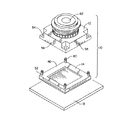
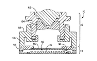
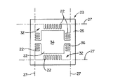
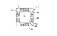
| JP2004260155A (ja) | リードレスリードフレーム電子パッケージ及びこれを組み込んだセンサモジュール | |
| US20070108561A1 (en) | Image sensor chip package | |
| US7595839B2 (en) | Image sensor chip packaging method | |
| JPH08107167A (ja) | 半導体装置 | |
| JP2003032557A (ja) | 固体撮像装置及びその製造方法 | |
| KR101008534B1 (ko) | 전력용 반도체모듈패키지 및 그 제조방법 | |
| US7429783B2 (en) | Image sensor package | |
| JP3748799B2 (ja) | 電子部品パッケージ及びその実装方法 | |
| JP4138436B2 (ja) | 光モジュール、回路基板及び電子機器 | |
| KR20050018381A (ko) | 고체 촬상용 반도체 장치 및 그 제조방법 | |
| KR100927423B1 (ko) | 글라스 캡 몰딩 패키지 및 그 제조방법, 그리고 카메라모듈 | |
| JP2025162943A (ja) | 画像撮像モジュール及び携帯電子装置 |
Legal Events
| Date | Code | Title | Description |
|---|---|---|---|
| A521 | Request for written amendment filed |
Free format text: JAPANESE INTERMEDIATE CODE: A523 Effective date: 20070206 |
|
| A621 | Written request for application examination |
Free format text: JAPANESE INTERMEDIATE CODE: A621 Effective date: 20070206 |
|
| A711 | Notification of change in applicant |
Free format text: JAPANESE INTERMEDIATE CODE: A711 Effective date: 20070727 |
|
| RD03 | Notification of appointment of power of attorney |
Free format text: JAPANESE INTERMEDIATE CODE: A7423 Effective date: 20070803 |
|
| A711 | Notification of change in applicant |
Free format text: JAPANESE INTERMEDIATE CODE: A711 Effective date: 20080222 |
|
| A521 | Request for written amendment filed |
Free format text: JAPANESE INTERMEDIATE CODE: A821 Effective date: 20080606 |
|
| RD02 | Notification of acceptance of power of attorney |
Free format text: JAPANESE INTERMEDIATE CODE: A7422 Effective date: 20080606 |
|
| A977 | Report on retrieval |
Free format text: JAPANESE INTERMEDIATE CODE: A971007 Effective date: 20100201 |
|
| A131 | Notification of reasons for refusal |
Free format text: JAPANESE INTERMEDIATE CODE: A131 Effective date: 20100209 |
|
| A02 | Decision of refusal |
Free format text: JAPANESE INTERMEDIATE CODE: A02 Effective date: 20100629 |