JP2004253448A - 電力用半導体装置 - Google Patents
電力用半導体装置 Download PDFInfo
- Publication number
- JP2004253448A JP2004253448A JP2003039667A JP2003039667A JP2004253448A JP 2004253448 A JP2004253448 A JP 2004253448A JP 2003039667 A JP2003039667 A JP 2003039667A JP 2003039667 A JP2003039667 A JP 2003039667A JP 2004253448 A JP2004253448 A JP 2004253448A
- Authority
- JP
- Japan
- Prior art keywords
- terminal
- semiconductor device
- power semiconductor
- voltage side
- low
- Prior art date
- Legal status (The legal status is an assumption and is not a legal conclusion. Google has not performed a legal analysis and makes no representation as to the accuracy of the status listed.)
- Pending
Links
Images


Classifications
-
- H—ELECTRICITY
- H01—ELECTRIC ELEMENTS
- H01L—SEMICONDUCTOR DEVICES NOT COVERED BY CLASS H10
- H01L24/00—Arrangements for connecting or disconnecting semiconductor or solid-state bodies; Methods or apparatus related thereto
- H01L24/01—Means for bonding being attached to, or being formed on, the surface to be connected, e.g. chip-to-package, die-attach, "first-level" interconnects; Manufacturing methods related thereto
- H01L24/42—Wire connectors; Manufacturing methods related thereto
- H01L24/47—Structure, shape, material or disposition of the wire connectors after the connecting process
- H01L24/49—Structure, shape, material or disposition of the wire connectors after the connecting process of a plurality of wire connectors
-
- H—ELECTRICITY
- H01—ELECTRIC ELEMENTS
- H01L—SEMICONDUCTOR DEVICES NOT COVERED BY CLASS H10
- H01L2224/00—Indexing scheme for arrangements for connecting or disconnecting semiconductor or solid-state bodies and methods related thereto as covered by H01L24/00
- H01L2224/01—Means for bonding being attached to, or being formed on, the surface to be connected, e.g. chip-to-package, die-attach, "first-level" interconnects; Manufacturing methods related thereto
- H01L2224/02—Bonding areas; Manufacturing methods related thereto
- H01L2224/04—Structure, shape, material or disposition of the bonding areas prior to the connecting process
- H01L2224/06—Structure, shape, material or disposition of the bonding areas prior to the connecting process of a plurality of bonding areas
- H01L2224/0601—Structure
- H01L2224/0603—Bonding areas having different sizes, e.g. different heights or widths
-
- H—ELECTRICITY
- H01—ELECTRIC ELEMENTS
- H01L—SEMICONDUCTOR DEVICES NOT COVERED BY CLASS H10
- H01L2224/00—Indexing scheme for arrangements for connecting or disconnecting semiconductor or solid-state bodies and methods related thereto as covered by H01L24/00
- H01L2224/01—Means for bonding being attached to, or being formed on, the surface to be connected, e.g. chip-to-package, die-attach, "first-level" interconnects; Manufacturing methods related thereto
- H01L2224/42—Wire connectors; Manufacturing methods related thereto
- H01L2224/47—Structure, shape, material or disposition of the wire connectors after the connecting process
- H01L2224/48—Structure, shape, material or disposition of the wire connectors after the connecting process of an individual wire connector
- H01L2224/481—Disposition
- H01L2224/48135—Connecting between different semiconductor or solid-state bodies, i.e. chip-to-chip
- H01L2224/48137—Connecting between different semiconductor or solid-state bodies, i.e. chip-to-chip the bodies being arranged next to each other, e.g. on a common substrate
-
- H—ELECTRICITY
- H01—ELECTRIC ELEMENTS
- H01L—SEMICONDUCTOR DEVICES NOT COVERED BY CLASS H10
- H01L2224/00—Indexing scheme for arrangements for connecting or disconnecting semiconductor or solid-state bodies and methods related thereto as covered by H01L24/00
- H01L2224/01—Means for bonding being attached to, or being formed on, the surface to be connected, e.g. chip-to-package, die-attach, "first-level" interconnects; Manufacturing methods related thereto
- H01L2224/42—Wire connectors; Manufacturing methods related thereto
- H01L2224/47—Structure, shape, material or disposition of the wire connectors after the connecting process
- H01L2224/49—Structure, shape, material or disposition of the wire connectors after the connecting process of a plurality of wire connectors
- H01L2224/491—Disposition
- H01L2224/4911—Disposition the connectors being bonded to at least one common bonding area, e.g. daisy chain
- H01L2224/49113—Disposition the connectors being bonded to at least one common bonding area, e.g. daisy chain the connectors connecting different bonding areas on the semiconductor or solid-state body to a common bonding area outside the body, e.g. converging wires
-
- H—ELECTRICITY
- H01—ELECTRIC ELEMENTS
- H01L—SEMICONDUCTOR DEVICES NOT COVERED BY CLASS H10
- H01L2224/00—Indexing scheme for arrangements for connecting or disconnecting semiconductor or solid-state bodies and methods related thereto as covered by H01L24/00
- H01L2224/01—Means for bonding being attached to, or being formed on, the surface to be connected, e.g. chip-to-package, die-attach, "first-level" interconnects; Manufacturing methods related thereto
- H01L2224/42—Wire connectors; Manufacturing methods related thereto
- H01L2224/47—Structure, shape, material or disposition of the wire connectors after the connecting process
- H01L2224/49—Structure, shape, material or disposition of the wire connectors after the connecting process of a plurality of wire connectors
- H01L2224/491—Disposition
- H01L2224/4912—Layout
- H01L2224/49171—Fan-out arrangements
-
- H—ELECTRICITY
- H01—ELECTRIC ELEMENTS
- H01L—SEMICONDUCTOR DEVICES NOT COVERED BY CLASS H10
- H01L2924/00—Indexing scheme for arrangements or methods for connecting or disconnecting semiconductor or solid-state bodies as covered by H01L24/00
- H01L2924/19—Details of hybrid assemblies other than the semiconductor or other solid state devices to be connected
- H01L2924/191—Disposition
- H01L2924/19101—Disposition of discrete passive components
- H01L2924/19107—Disposition of discrete passive components off-chip wires
-
- H—ELECTRICITY
- H01—ELECTRIC ELEMENTS
- H01L—SEMICONDUCTOR DEVICES NOT COVERED BY CLASS H10
- H01L2924/00—Indexing scheme for arrangements or methods for connecting or disconnecting semiconductor or solid-state bodies as covered by H01L24/00
- H01L2924/30—Technical effects
- H01L2924/301—Electrical effects
- H01L2924/30107—Inductance
Landscapes
- Engineering & Computer Science (AREA)
- Computer Hardware Design (AREA)
- Microelectronics & Electronic Packaging (AREA)
- Power Engineering (AREA)
- Inverter Devices (AREA)
- Power Conversion In General (AREA)
Abstract
【解決手段】電力用半導体装置11aにおいて、低圧側スイッチング素子を駆動する制御回路IC2はそれらのスイッチング素子をオフする際の基準電位を与えるための出力基準端子VN0を有する。また、電力用半導体装置11aは低圧側スイッチング素子の低圧側端子(エミッタ端子)S1a〜S3aが接続された外部端子Nを有する。出力基準端子VN0は、その外部端子Nにおいて低圧側スイッチング素子S1〜S3の低圧側端子が接続される部分P1と、外部端子Nの外部に露出した部分P2との間に接続される。
【選択図】 図1
Description
【発明の属する技術分野】
本発明は電力用半導体装置に関し、特に、電力用半導体装置におけるサージ電圧保護に関する。
【0002】
【従来の技術】
電力用半導体装置は、スイッチング素子を低圧側及び高圧側に直列に接続したハーフブリッジ回路を複数並列に接続してなるインバータ回路と、低圧側及び高圧側のスイッチング素子をそれぞれ駆動する制御回路とを備える(例えば特許文献1参照)。
【0003】
一般に、低圧側スイッチング素子を駆動する制御回路は、低圧側スイッチング素子のゲートに接続されその電位を制御する出力端子と、低圧側スイッチング素子のエミッタに接続され、低圧側スイッチング素子をオフさせる際の基準電位を出力する出力基準端子とを備える。制御回路は、低圧側スイッチング素子をオンさせるときは、出力端子から低圧側スイッチング素子をオンさせるのに十分高い電圧の信号を出力し、一方、低圧側スイッチング素子をオフさせるときは、出力端子の電位を出力基準端子の電位と同電位となるよう制御する。
【0004】
制御回路の出力基準端子は低圧側スイッチング素子のエミッタ端子に接続されるが、このとき、出力基準端子VN0は、低圧側スイッチング素子のエミッタ端子に直接ワイヤボンド接続されるか、又は、配線フレームや配線パターンを介してワイヤボンド接続される。
【0005】
電力用半導体装置内の全ての低圧側スイッチング素子のエミッタ端子は共通の外部端子に接続される。電力用半導体装置の外部において、その外部端子には過電流検出用のシャント抵抗の一端が接続される。シャント抵抗の他端はグランド電位(接地電位)を与えるグランド端子に接続される。
【0006】
なお、以上のような構成を有する半導体装置に関する先行技術として特許文献2、3に開示のものがある。
【0007】
【特許文献1】
特開平10−42575号公報
【特許文献2】
特開平2001−274322号公報
【特許文献3】
特開平2002−64180号公報
【0008】
【発明が解決しようとする課題】
以上の構成を有する従来の半導体装置では、スイッチング動作時に、低圧側スイッチング素子のエミッタ端子と外部端子とを接続する配線のインダクタンスと、その外部端子とシャント抵抗とを接続する配線のインダクタンスと、シャント抵抗自身の内部インダクタンスとにサージ電圧が発生した場合、そのサージ電圧は出力基準端子と電力用半導体装置のグランド端子との間に印加される。よって、低圧側スイッチング素子を駆動する制御回路にこのサージ電圧が印加され、制御回路が破壊される場合がある。
【0009】
本発明は上記課題を解決すべくなされたものであり、その目的とするところは、サージ電圧による制御回路の破壊を防止する電力用半導体装置を提供することにある。
【0010】
【課題を解決するための手段】
本発明に係る電力用半導体装置は、直列接続されたスイッチング素子からなるハーフブリッジ回路が複数並列に接続されてなるインバータ回路と、ハーフブリッジ回路において低圧側に接続されたスイッチング素子を駆動する制御回路と、低圧側スイッチング素子の低圧側の端子が接続され、一部が外部に露出した外部端子とを備えた電力用半導体装置である。制御回路は低圧側スイッチング素子をオフする際の基準電位を与えるための基準端子を有する。その基準端子は外部端子において低圧側スイッチング素子の低圧側の端子が接続される部分と、外部端子の外部に露出した部分との間に接続される。
【0011】
【発明の実施の形態】
以下添付の図面を参照して、本発明に係る電力用半導体装置の実施の形態を詳細に説明する。
【0012】
実施の形態1.
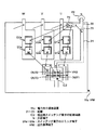
図1は本実施形態の電力用半導体装置の出力端子U、V、W近傍の配線状況を示した図である。図2は本発明に係る電力用半導体装置の構成を示した図である。図2に示すように、電力用半導体装置は3相交流電圧を出力する電力用パワーモジュール(IPM)であり、複数のスイッチング素子S1〜S4からなるインバータ回路と、それらのスイッチング素子を駆動する制御回路IC1、IC2とを備える。各スイッチング素子S1〜S4にはダイオードD1〜D4がそれぞれ並列に逆接続される。
【0013】
制御回路IC1はU相の高圧側のスイッチング素子S4を駆動する。なお、図2において、V相、W相においては、高圧側のスイッチング素子およびそれを駆動する制御回路は回路Q1、Q2に含まれる。
【0014】
制御回路IC2は低圧側のスイッチング素子S1〜S3を駆動し、そのため、出力端子OUT1〜OUT3を有している。
【0015】
低圧側スイッチング素子S1〜S3のエミッタ端子は電力半導体装置11aの外部端子Nに接続される。外部端子Nは過電流検出を行なうためのシャント抵抗R1を介してグランド電位(接地電位)を与えるグランド端子N1に接続される。
【0016】
図2において、インダクタンスL1、L2、L3は、それぞれ低圧側スイッチング素子S1、S2、S3のエミッタ端子と外部端子Nを接続する配線のインダクタンス成分を示す。インダクタンスL4は端子Nとシャント抵抗R1間の配線のインダクタンス成分、インダクタンスL5はシャント抵抗R1と端子N1間の配線のインダクタンス成分を示す。
【0017】
シャント抵抗R1に発生する電圧VRは、抵抗R2とコンデンサC1からなるフィルタ回路及び過電流検知端子CINを介して制御回路IC2に入力される。電圧VRが所定値を超えると制御回路IC2は過電流保護機能を作動し、その出力OUT1〜OUT3を遮断する。
【0018】
制御回路IC2は低圧側スイッチング素子S1〜S3のオフさせる際の基準電位を与える出力基準端子VN0を有する。具体的には、制御回路IC2はスイッチング素子S1〜S3をオフさせる際は、出力端子OUT1〜OUT3の電位を出力基準端子VN0の電位と同じになるように制御する。すなわち、制御回路IC2はスイッチング素子S1〜S3をオフさせる際は、その内部において出力基準端子VN0とそれぞれの出力端子OUT1〜OUT3とを短絡する。
【0019】
図1を参照し、U相電圧を外部に出力するための外部端子Uには、スイッチング素子S1のエミッタ端子S1aと、スイッチング素子S1に逆並列接続されたダイオードD1のアノード端子D1aとが接続されている。同様に、V相電圧を外部に出力するための外部端子Vには、スイッチング素子S2のエミッタ端子S2aと、スイッチング素子S2に逆並列接続されたダイオードD2のアノード端子D2aとが接続されている。W相電圧を外部に出力するための外部端子Wには、スイッチング素子S3のエミッタ端子S3aと、スイッチング素子S3に逆並列接続されたダイオードD3のアノード端子D3aとが接続されている。
【0020】
出力基準端子VN0は外部端子Nに接続される。より詳細には、図1に示すように、出力基準端子VN0は、配線21及びボンディングワイヤ23を介して、外部端子Nを構成する導電部材22の電力用半導体装置内側にある低圧側スイッチング素子S1〜S3のエミッタ端子が接続される部分P1と、導電部材22の外部に露出した部分P2との間の部分に接続されている。このように、出力基準端子VN0を、外部端子N内の低圧側スイッチング素子S1〜S3のエミッタ端子が接続される部分P1よりも、より外部側に近いところに接続する。これにより、制御回路IC2の出力基準端子VN0には、低圧側スイッチング素子S1〜S3の各エミッタ端子と外部端子N間の配線のインダクタンスL1、L2、L3により発生するサージ電圧が印加されることがなくなるため、サージ電圧による制御回路の破壊を防止でき、サージ破壊耐量を向上できる。
【0021】
実施の形態2.
図3は本発明に係る電力用半導体装置の別の構成を示した図である。また、図4は本実施形態の電力用半導体装置11bの出力端子U、V、W近傍の配線の状況を示した図である。
【0022】
本実施形態の電力用半導体装置11bは、実施の形態1の構成においてさらに外部端子Vnoを備える。外部端子Vnoは電力用半導体装置11b内において制御回路IC2の出力基準端子VN0と接続され、電力用半導体装置11b外部においてシャント抵抗R1における端子Nとの接続端に接続される。このような出力基準端子VN0に接続する外部端子Vnoを設けたことにより、出力基準端子VN0を配線インダクタンスの影響を低減できる所望の位置に接続することが可能となる。
【0023】
このように、制御回路IC2の出力基準端子VN0はシャント抵抗R1における端子Nとの接続端に接続されることにより、インダクタンスL1〜L3で発生するサージ電圧に加え、端子Nとシャント抵抗R1間の配線のインダクタンスL4で発生するサージ電圧の制御回路IC2への印加を防止でき、実施の形態1に比してより効果的にサージ電圧による制御回路の破壊を防止でき、さらにサージ破壊耐量を向上できる。
【0024】
実施の形態3.
図5は本発明に係る電力用半導体装置のさらに別の構成を示した図である。本実施形態の電力用半導体装置11cは実施の形態1の構成においてさらに外部端子Vnoを備える。外部端子Vnoは電力用半導体装置11c内において制御回路IC2の出力基準端子VN0と接続され、電力用半導体装置11c外部においてグランド電位を与えるグランド端子N1に接続される。
【0025】
このように、制御回路IC2の出力基準端子VN0がグランド電位を与えるグランド端子N1に接続されることにより、インダクタンス成分L1〜L3、L4で発生するサージ電圧に加えてシャント抵抗R1のインダクタンス成分L5で発生するサージ電圧の制御回路IC2への印加を防止でき、実施の形態1、2に比してさらに効果的にサージ電圧による制御回路の破壊を防止でき、よりサージ破壊耐量を向上できる。
【0026】
なお、本実施形態の回路構成では、低圧側スイッチング素子S1〜S3のエミッタ端子と制御回路IC2の出力基準端子VN0との間に直列にシャント抵抗が挿入されることになるが、このシャント抵抗値を考慮に入れて制御回路IC2内部のゲート抵抗値を適宜設定することで適切なスイッチング速度を実現できる。
【0027】
なお、上記の各実施形態において配線は配線フレームや配線パターン等で実現される。
【0028】
【発明の効果】
本発明の電力用半導体装置によれば、低圧側スイッチング素子を駆動する制御回路に対する、配線のインダクタンス成分により生じるサージ電圧の影響を排除できるため、サージ電圧による制御回路の破壊を防止でき、サージ電圧耐量を向上できる。
【図面の簡単な説明】
【図1】実施の形態1の電力用半導体装置の出力端子U、V、W近傍の配線状況を示した図
【図2】本発明の実施の形態1における電力用半導体装置の回路図
【図3】本発明の実施の形態2における電力用半導体装置の回路図
【図4】実施の形態2の電力用半導体装置の出力端子U、V、W近傍の配線状況を示した図
【図5】本発明の実施の形態3における電力用半導体装置の回路図
【符号の説明】
11a,11b,11c 電力用半導体装置(IPM)、 CIN 過電流検出端子、 S1〜S3 低圧側スイッチ、 N 外部端子、 N1 基準電位を与える端子、 L1〜L3,L4 配線のインダクタンス成分、 L5 シャント抵抗のインダクタンス成分、 R1 シャント抵抗、 Vno 外部端子
Claims (4)
- 直列接続されたスイッチング素子からなるハーフブリッジ回路が複数並列に接続されてなるインバータ回路と、前記ハーフブリッジ回路において低圧側に接続されたスイッチング素子を駆動する制御回路と、前記低圧側スイッチング素子の低圧側の端子が接続され、一部が外部に露出した外部端子とを備えた電力用半導体装置において、
前記制御回路は低圧側スイッチング素子をオフする際の基準電位を与えるための基準端子を有し、該基準端子は、前記外部端子において前記低圧側スイッチング素子の低圧側の端子が接続される部分と、前記外部端子の外部に露出した部分との間に接続されることを特徴とする請求項1記載の電力用半導体装置。 - 直列接続されたスイッチング素子からなるハーフブリッジ回路が複数並列に接続されてなるインバータ回路と、前記ハーフブリッジ回路において低圧側に接続されたスイッチング素子を駆動する制御回路と、前記低圧側スイッチング素子の低圧側の主電極が接続される第1の外部端子とを備えた電力用半導体装置において、
さらに、第2の外部端子を備え、
前記制御回路は低圧側スイッチング素子をオフする際の基準電位を与えるための基準端子を有し、該基準端子は前記第2の外部端子に接続されたことを特徴とする電力用半導体装置。 - 前記第1の外部端子に電流検出用のシャント抵抗の一端が接続され、前記第2の外部端子に該シャント抵抗の一端が接続されることを特徴とする請求項2記載の電力用半導体装置。
- 前記第1の外部端子に電流検出用のシャント抵抗の一端が接続され、前記シャント抵抗の他端にグランド電位を与えるグランド端子が接続され、前記第2の外部端子に前記グランド端子が接続されることを特徴とする請求項2記載の電力用半導体装置。
Priority Applications (1)
| Application Number | Priority Date | Filing Date | Title |
|---|---|---|---|
| JP2003039667A JP2004253448A (ja) | 2003-02-18 | 2003-02-18 | 電力用半導体装置 |
Applications Claiming Priority (1)
| Application Number | Priority Date | Filing Date | Title |
|---|---|---|---|
| JP2003039667A JP2004253448A (ja) | 2003-02-18 | 2003-02-18 | 電力用半導体装置 |
Publications (1)
| Publication Number | Publication Date |
|---|---|
| JP2004253448A true JP2004253448A (ja) | 2004-09-09 |
Family
ID=33023780
Family Applications (1)
| Application Number | Title | Priority Date | Filing Date |
|---|---|---|---|
| JP2003039667A Pending JP2004253448A (ja) | 2003-02-18 | 2003-02-18 | 電力用半導体装置 |
Country Status (1)
| Country | Link |
|---|---|
| JP (1) | JP2004253448A (ja) |
Cited By (2)
| Publication number | Priority date | Publication date | Assignee | Title |
|---|---|---|---|---|
| JP2017228683A (ja) * | 2016-06-23 | 2017-12-28 | ルネサスエレクトロニクス株式会社 | 電子装置 |
| WO2020157963A1 (ja) * | 2019-02-01 | 2020-08-06 | 三菱電機株式会社 | 半導体装置および電力変換装置 |
-
2003
- 2003-02-18 JP JP2003039667A patent/JP2004253448A/ja active Pending
Cited By (4)
| Publication number | Priority date | Publication date | Assignee | Title |
|---|---|---|---|---|
| JP2017228683A (ja) * | 2016-06-23 | 2017-12-28 | ルネサスエレクトロニクス株式会社 | 電子装置 |
| WO2020157963A1 (ja) * | 2019-02-01 | 2020-08-06 | 三菱電機株式会社 | 半導体装置および電力変換装置 |
| JPWO2020157963A1 (ja) * | 2019-02-01 | 2021-10-21 | 三菱電機株式会社 | 半導体装置および電力変換装置 |
| JP7069358B2 (ja) | 2019-02-01 | 2022-05-17 | 三菱電機株式会社 | 半導体装置および電力変換装置 |
Similar Documents
| Publication | Publication Date | Title |
|---|---|---|
| JP3193827B2 (ja) | 半導体パワーモジュールおよび電力変換装置 | |
| JP4682007B2 (ja) | 電力用半導体装置 | |
| JP4313658B2 (ja) | インバータ回路 | |
| US6593781B2 (en) | Power semiconductor device | |
| JPH02266712A (ja) | 半導体装置 | |
| US7978453B2 (en) | Low side driver with short to battery protection | |
| JP2000350465A (ja) | 3レベルインバータ | |
| JP3762491B2 (ja) | 高電圧駆動回路 | |
| JP6107949B2 (ja) | 半導体モジュール | |
| JP4847707B2 (ja) | 電力用半導体装置 | |
| JP2003309982A (ja) | 電力用半導体装置 | |
| JP2008061339A (ja) | インバータ回路 | |
| JP2004253448A (ja) | 電力用半導体装置 | |
| JP4770063B2 (ja) | Ipm回路 | |
| JP4278440B2 (ja) | 電力用半導体装置および該装置に用いられる半導体集積回路装置 | |
| JPH10145206A (ja) | 半導体装置の保護回路 | |
| KR20200123385A (ko) | 집적형 서지 전압 제한 요소를 구비한 전력 모듈 | |
| CN115913198B (zh) | 多驱动通道高压集成电路和半导体电路 | |
| US11606090B2 (en) | Semiconductor device | |
| WO2022075000A1 (ja) | 半導体モジュール | |
| JP7435359B2 (ja) | 負荷駆動回路 | |
| JP2021190640A (ja) | パワーモジュール | |
| JP2022181192A (ja) | インバータ装置およびそれを備えた車両 | |
| JPH03236280A (ja) | 半導体装置 | |
| JPH04334995A (ja) | 直流ブラシレスモータのインバータ回路 |
Legal Events
| Date | Code | Title | Description |
|---|---|---|---|
| A621 | Written request for application examination |
Free format text: JAPANESE INTERMEDIATE CODE: A621 Effective date: 20050726 |
|
| A977 | Report on retrieval |
Free format text: JAPANESE INTERMEDIATE CODE: A971007 Effective date: 20070531 |
|
| A131 | Notification of reasons for refusal |
Free format text: JAPANESE INTERMEDIATE CODE: A131 Effective date: 20070612 |
|
| A521 | Request for written amendment filed |
Free format text: JAPANESE INTERMEDIATE CODE: A523 Effective date: 20070808 |
|
| A131 | Notification of reasons for refusal |
Free format text: JAPANESE INTERMEDIATE CODE: A131 Effective date: 20081028 |
|
| A521 | Request for written amendment filed |
Free format text: JAPANESE INTERMEDIATE CODE: A523 Effective date: 20081211 |
|
| A02 | Decision of refusal |
Free format text: JAPANESE INTERMEDIATE CODE: A02 Effective date: 20090120 |